The Optical Axis Alone Won’t Show It: Redrawing CPO Across Three Budgets, Energy, Heat, and Reach
$NVDA $LITE $COHR $AXTI $TSEM $CRDO $ALAB $MRVL $AAOI $VICR $MPWR $GLW $POET $LWLG | Optical Interconnect Value Chain Across Three Budgets

The optical interconnect value chain usually gets drawn as a single line. One optical axis running up from the InP substrate through the laser to the optical engine. That picture cannot explain why CPO is arriving now, when it goes to volume, or who captures the margin. CPO is a co-design problem where three physical budgets are bound together at once: energy (pJ/bit), heat (junction temperature), and reach (propagation loss plus coupling loss). The cost of moving one bit depends on where you draw the measurement boundary (module, port, link, engine), but retimed pluggable optics sit roughly in the 10 pJ/bit range while CPO-class designs target around 5 pJ/bit or below [1][2][3]. Over the same window, rack power climbs from about 40kW in the H100 generation to roughly 600kW for Rubin Ultra Kyber, and 800V HVDC is designed with 1MW-class racks in mind [4]. The switch ASIC junction sits near 100C inside the same package as the optics [5]. The conclusion up front: CPO ramp timing is set not by InP supply but by the moment 800V power, liquid cooling, ELS reliability, and optical engine qualification all open together. This piece redraws the value chain at the point where those three budgets collide. Relevant tickers are in the subtitle above.
Contents
Intro: the market already voted with one leg
Three budgets: energy, heat, reach
Everyone sees the InP bottleneck. But
Splitting one rack into dollars and watts
The energy axis: where copper dies and DSP disappears
The thermal axis: the gate that sets CPO’s schedule
The reach (optical) axis: the supply chain everyone draws, resorted
Value migration: copper earns the most right before it dies
Scenarios, monitoring, closing
References & Sources
Intro: the market already voted with one leg
At GTC in March 2026, Jensen Huang put three big threads on stage. Rubin, Feynman, and CPO. The first two are GPU generation names. The third is not a GPU but the way GPUs get connected. On the same stage NVIDIA stated that the CPO switch had moved into a “volume production plan” phase, and the company laid out an AI systems demand outlook of about one trillion dollars through 2027 [6]. That trillion is not a CPO order book. It is total AI systems demand across the Blackwell and Rubin platforms, and CPO has moved up into that roadmap as a core networking layer.
This system-level reshaping, where workloads split from training into inference and agentic, and GPU, host CPU, and inference accelerator get divided across several foundries into a multi-anchor structure, was the subject of an earlier piece, “The GPU era ran on TSMC, the inference era runs on multiple foundries”. Its conclusion was that as chips split apart, the next bottleneck moves from “who makes the chips” to “what fabric connects these chips.” This piece looks at exactly that fabric, optical interconnect.

The signal is already in the tape. In NVIDIA’s results, the networking contribution started growing ahead of compute, and the optical, power, and cooling names were repriced one after another over the past year. Up to here it is tempting to label the whole thing the “optical cycle.” The moment you do, you see only half of it.
Turn the lens from optics to electricity and the underlying problem shows up. Why convert copper to light now? Because the energy it takes to move one bit over copper has crossed the point where it costs more than the computation that bit represents. That is the real starting point of this cycle, and it is not a story about optical companies alone.
The market voted with one leg on “optics is good.” The other leg is electricity and heat.
Three budgets: energy, heat, reach
For an investor, the frame that explains CPO better than a supply chain is a budget. An engineer designing an AI rack has to satisfy three budgets at once. Break any one of them and the system does not stand, no matter how good the rest is. The limits of copper that the industry flagged through 2026 sort into the same three branches: power delivery, electrical bandwidth, and distance [7].
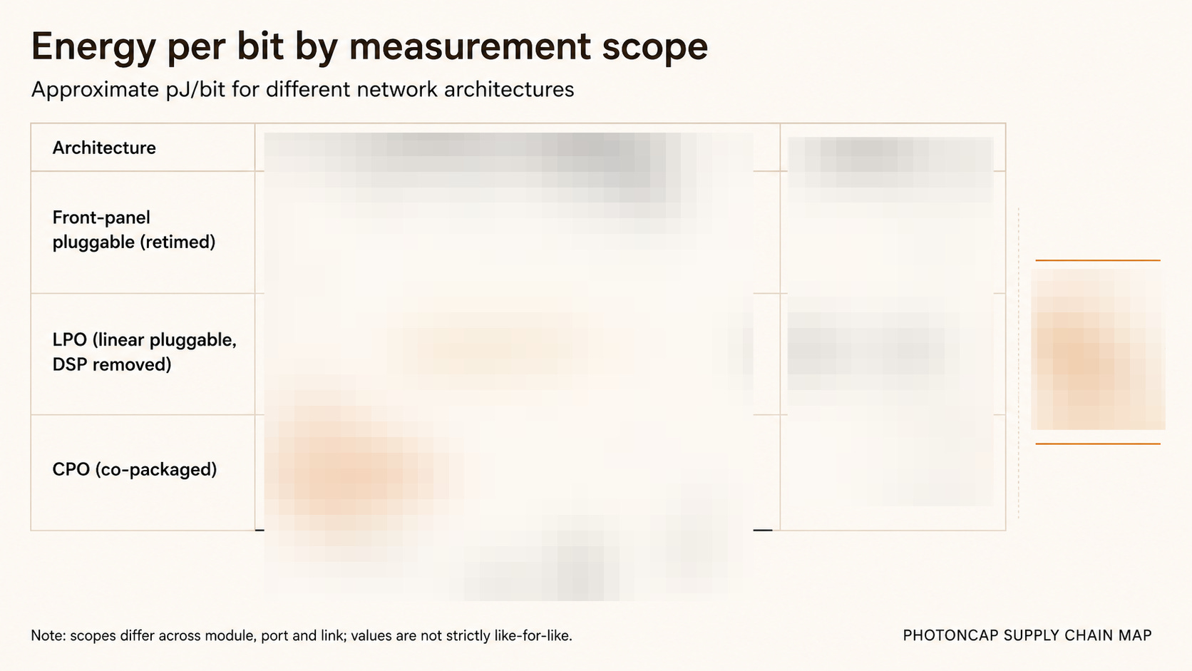
First, the energy budget. The farther you push a signal over SerDes, the heavier the equalization and retiming burden, and power rises quickly with distance and speed. The economic, power-efficient reach of passive copper shrinks fast each generation. In a traditional pluggable, the electrical path loss between the host ASIC and the module runs to about 22dB, and at 200G/lane retiming becomes mandatory [8]. CPO cuts that path from inches to millimeters, lowering loss and power together, because light covers the same distance for almost free. The numbers make the gap clear. The values shift with the measurement boundary, but retimed pluggable optics sit roughly in the 10 pJ/bit range, while CPO-class designs that bring the optics inside the package target around 5 pJ/bit or below [1][2][3]. NVIDIA put the per-port CPO power saving at about 3.5x at its 2025 Spectrum-X Photonics announcement [9]. NVLink scale-up bandwidth runs at 1.8 TB/s per GPU on Blackwell (NVLink 5) and 3.6 TB/s on Rubin (NVLink 6), doubling each generation [10], and pushing that bandwidth over copper blows the power budget first.
Second, the thermal budget. The “co” in co-packaged is the heart of the problem. The moment you place optics next to a hot ASIC, you get a thermal conflict. Lasers are extremely temperature-sensitive. When temperature drifts, the lasing wavelength shifts, threshold current rises, and lifetime falls steeply [11]. Yet the switch ASIC dumps hundreds of watts. On the limits Intel laid out, the switch chip junction needs to stay below 105C and the optical module EIC junction below 100C, and in a 51.2 Tb/s CPO system the switch junction lands near 97C [5]. To avoid that conflict, the laser gets pulled out of the package and placed far away, which is the external laser source (ELS) architecture [11]. ELS is not optical-design elegance. It is a compromise forced by heat.
Third, the reach budget. Light travels far, but not for free. To be precise, there are two kinds of loss. Propagation loss, which accumulates with distance along fiber and waveguide, and coupling loss, which is added at each interface where light crosses a medium, such as laser to fiber or fiber to PIC. Why this fiber-to-chip coupling is the last bottleneck of CPO packaging was the subject of an earlier piece, “The Last Millimeter: Fiber-to-Chip Coupling and the CPO Packaging Bottleneck”. Pull the laser far out and the combined link budget grows, and to cover it the launch power has to be high. That is why a CPO laser demands far higher output than a regular transceiver CW laser. This is where the optical axis running InP, laser, SOI, foundry shows up. The supply chain everyone draws.
![[PC101] Lecture 4:The Last Millimeter: Fiber-to-Chip Coupling and the CPO Packaging Bottleneck (Part 1)](https://substackcdn.com/image/fetch/$s_!qZxp!,w_140,h_140,c_fill,f_webp,q_auto:good,fl_progressive:steep,g_auto/https%3A%2F%2Fsubstack-post-media.s3.amazonaws.com%2Fpublic%2Fimages%2Fa743aebb-02e3-496d-95cf-0da2962050b1_3590x2099.png)
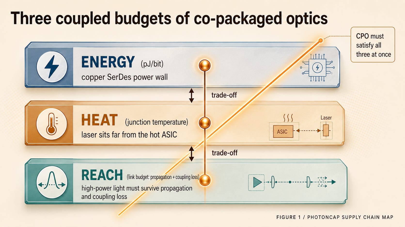
[Figure 1: The Three Budgets of Co-Packaged Optics, energy / thermal / reach as three coupled constraints]
The key point is that the three budgets are not independent. They are coupled. Pull the laser far out to solve heat and the reach budget worsens. Bring it close to shorten reach and the thermal budget breaks. Add optics to cut power and thermal density climbs again. CPO design comes down to satisfying these three constraints at the same time.
CPO is not about gathering optical components. It is about meeting three competing budgets at once.
Everyone sees the InP bottleneck. But
That InP substrate is tight is now common knowledge. Why AXT sits at the center of that bottleneck was the subject of an earlier piece, “AXT Inc. (AXTI) Deep Dive: The Hidden Bottleneck in AI Optical Interconnects”. The problem is that it does not set when CPO goes to volume. Timing is held by power and heat, not optical supply. You cannot place optics next to a 1500W ASIC until you have solved how to feed it and how to cool it.

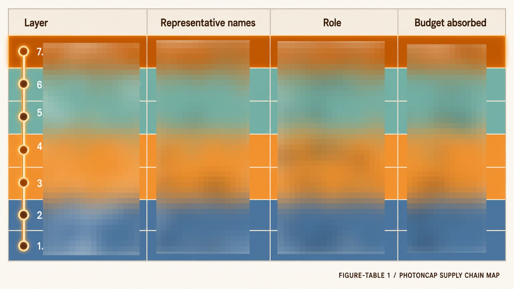
The bottleneck is not InP alone. Almost every layer across the three budgets has its own bottleneck and its own stock story, and PhotonCap has covered them layer by layer. On the reach axis alone, the last millimeter of fiber-to-chip coupling is in “The Last Millimeter”, the FAU and microlens supplier landscape is in “The COUPE Microlens Monopoly Is Real, But the Market Is Missing the Bigger Picture”, the photonics-SOI monopoly under the PIC is in “The Wafer That Used to Roll Around My Lab”, and the light-source maker that moved from cable-TV parts to AI optics is in “$AAOI, From $10 to $150”. On the thermal axis, the EO polymer that Tower chose is in “The Polymer That Tower Chose”. On the power axis, why Vicor’s vertical power delivery starts from a single line, P=I squared R, is in “P = I squared R”. POET at the optical engine integration step is in “$1.1M Revenue, $1.1B Market Cap”, and the picture of the whole system splitting from a single foundry into multi-anchor is in “The GPU Era Ran on TSMC”. This piece puts those layer-by-layer analyses back onto one coordinate system: energy, heat, and reach.
So this piece tracks three migrations. The power budget moves from 54V to 800V, the energy budget from the DSP retimer to the host and CPO, and the reach budget from the pluggable laser to ELS, the optical engine, and the foundry. Recast as three questions: split one rack into dollars and watts and what share is optical, and where does that share move each generation? On the energy axis, which component sees money leave first? And how much more does copper earn right before it dies?
Where the answers to these three questions meet is where winners and losers split. The body works through those intersections one by one.