
Citrini/Hunterbrook HIMX Report Analysis: Yes, the COUPE Microlens Monopoly Is Real. But the Market Is Missing the Bigger Picture.

Introduction
On March 12, Hunterbrook Media and Citrini Research dropped reports at the same time. Citrini published “Let There Be Light,” an optics/connectivity basket update for paid subscribers [16], while Hunterbrook released their investigative deep dive on Himax, “Stealth Supplier for NVIDIA’s Optics Revolution,” for free [1].
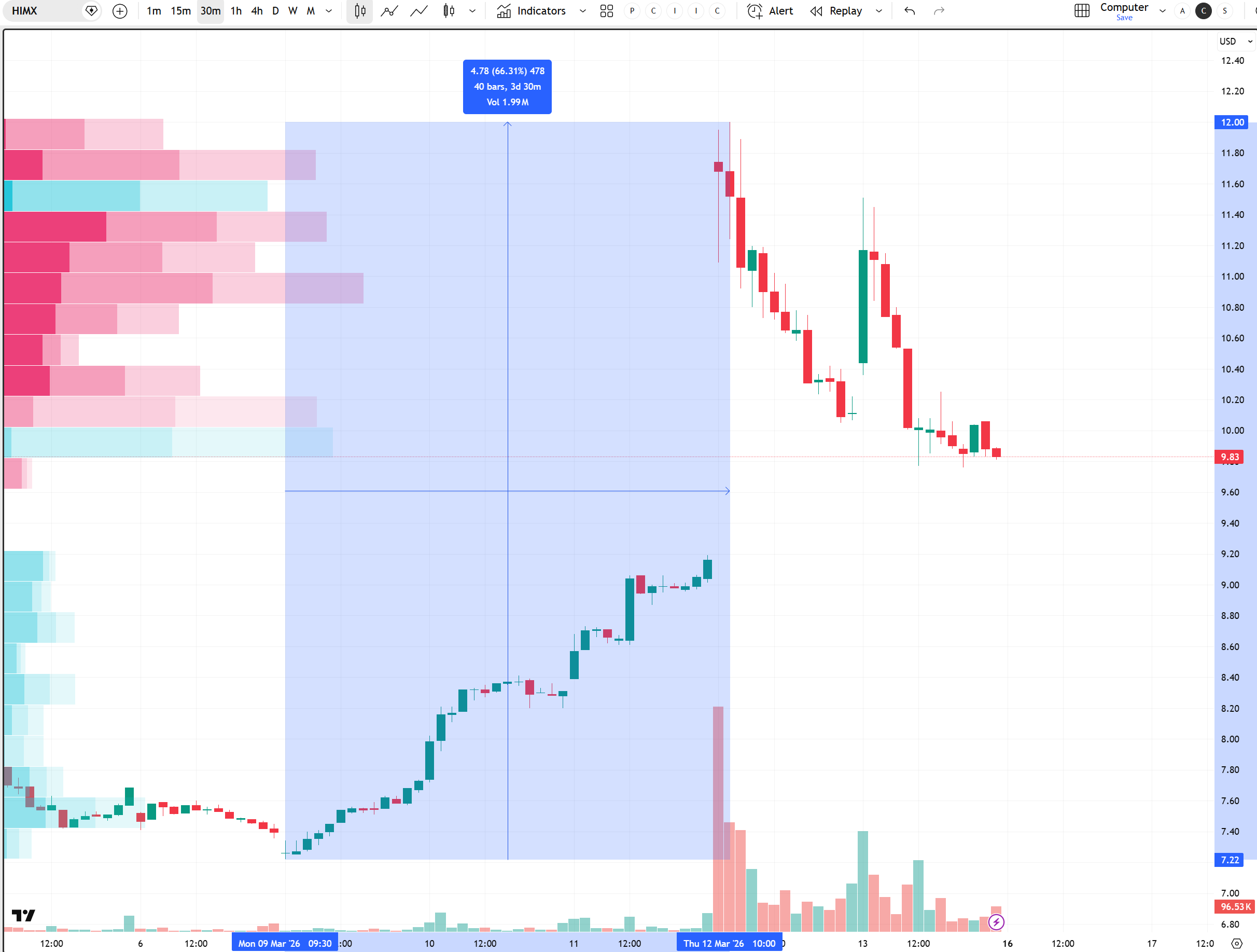
The price action told a story. HIMX started moving well before the report came out, climbing from $7.4 on March 6 to $9.15 by March 11. On March 11, when the report dropped, the stock spiked to $12 intraday before pulling back hard in the afternoon.
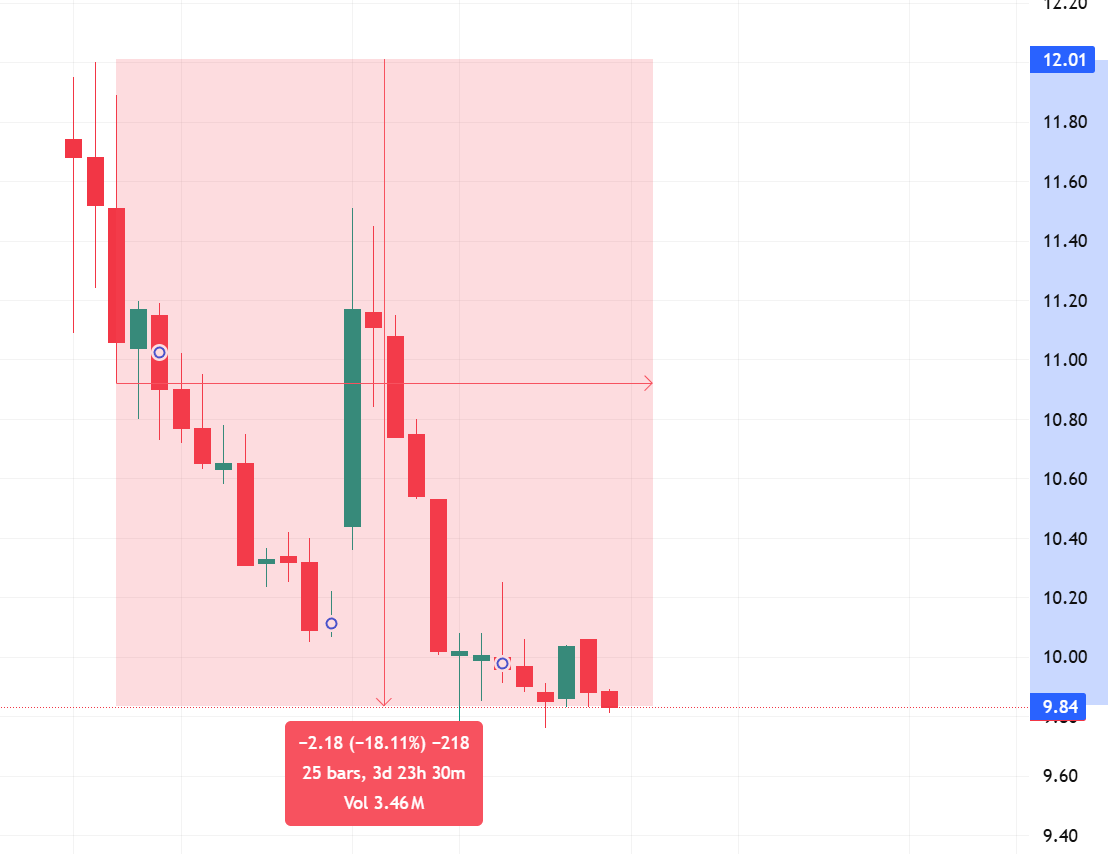
By March 13, it was down again to $9.84. Volume on March 12 hit 36 million shares, roughly 30x the daily average [17]. The fact that the stock was already running before the report landed is worth thinking about, especially given that Hunterbrook Capital disclosed a long position in HIMX [1].
“About 36 million HIMX shares exchanged hands on Thursday, about 30 times the stock’s average trading volume. Himax shares have gained for four consecutive sessions, rising 60%.”
The report makes two big claims. First, that Himax is the “sole supplier” of microlens arrays for NVIDIA’s CPO (Co-Packaged Optics) platform. Second, that Himax is likely supplying LCoS microdisplays and waveguides for Apple’s upcoming smart glasses.
Citrini also has photonics names in their own paid basket [16]. Both reports are high-quality research, but both come with financial interests attached. Keep that in mind.
The core thesis of this article: Himax being the sole microlens supplier for TSMC’s COUPE Gen 1 and Gen 2 is real. But the market is overestimating the scope of that monopoly. Microlens arrays are one layer inside the FAU. V-grooves and FAU assembly are commodity work. And when you zoom out to the full NVIDIA CPO ecosystem, COUPE is not the only path.
Today, I am going to walk through the four patents Hunterbrook cited, the Tianfeng Securities analysis, NVIDIA’s official CPO partner list, and the actual competitive landscape.
Background: CPO and FAU, Why They Matter
At GTC in March 2025, Jensen Huang laid out a striking number: networking alone inside a million-GPU AI factory would consume 180 megawatts. That is because each GPU needs six pluggable transceivers, each burning roughly 30 watts [2].
“The question is: how do we scale up now to millions of GPUs?” said the CEO. “Because if we have a million GPUs [we need] 6 million transceivers [consuming] 180 megawatts.”
NVIDIA’s answer is CPO. Instead of converting electrical signals to light in a separate external box, CPO handles the conversion right inside the network switch package. This eliminates the external transceiver and cuts power consumption by about 3.5x. It runs on TSMC’s COUPE (Compact Universal Photonic Engine) platform and uses micro ring modulators (MRM) [2][3][20].
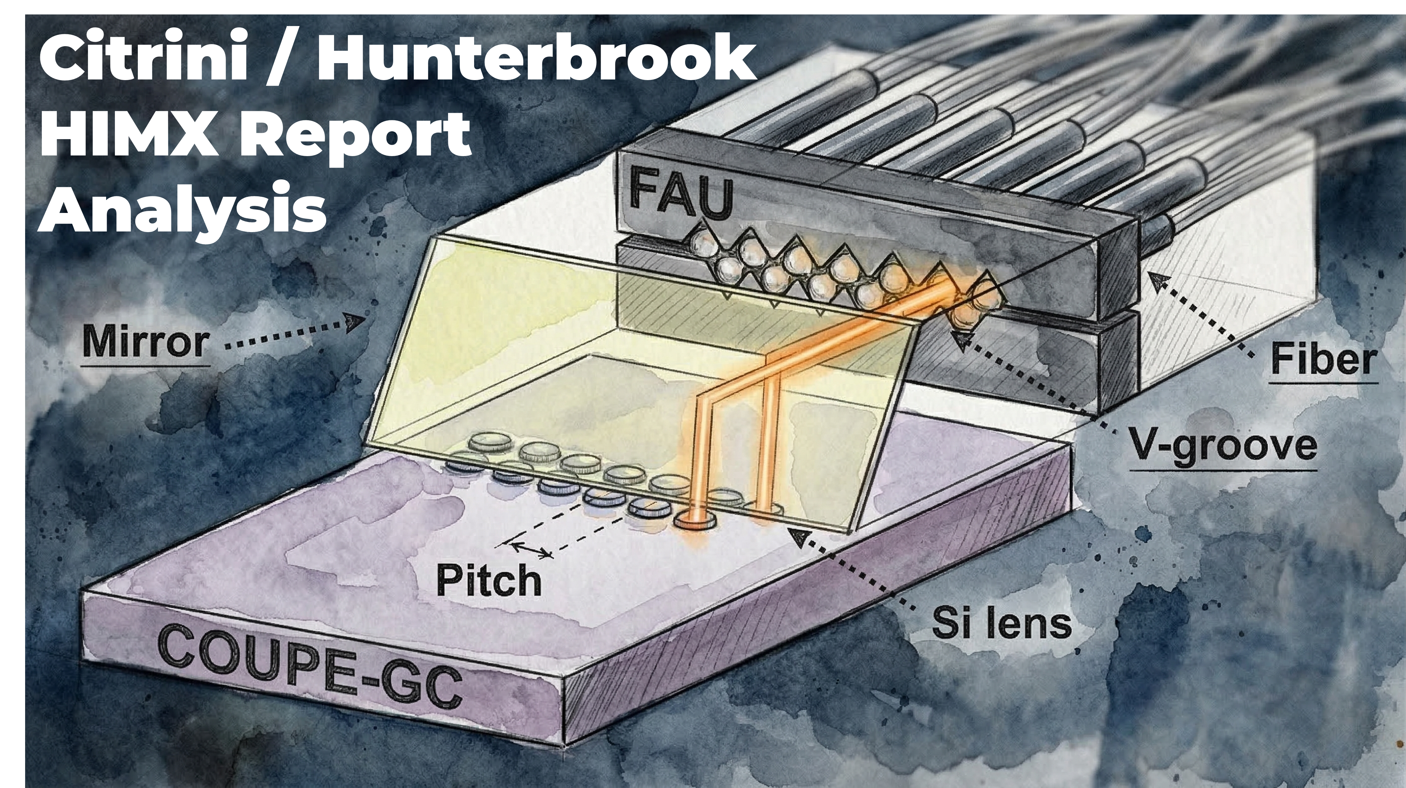
This is where the FAU (Fiber Array Unit) comes in. The COUPE optical engine shoots data-carrying laser light straight up. Something has to bend each beam 90 degrees and couple it into horizontal optical fibers thinner than a human hair. That “something” is a prism and a microlens array sitting inside the FAU. The V-groove substrate that holds the fibers in precise alignment is also part of the FAU [3].
For reference, you can see exactly where the FAU sits within a CPO module in our teardown of Marvell’s TX9190 at my latest article.
The Last Millimeter: Fiber-to-Chip Coupling and the CPO Packaging Bottleneck (Part 1)
·Welcome back. This is PhotonCap.

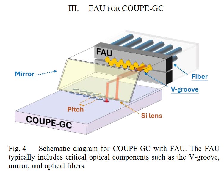
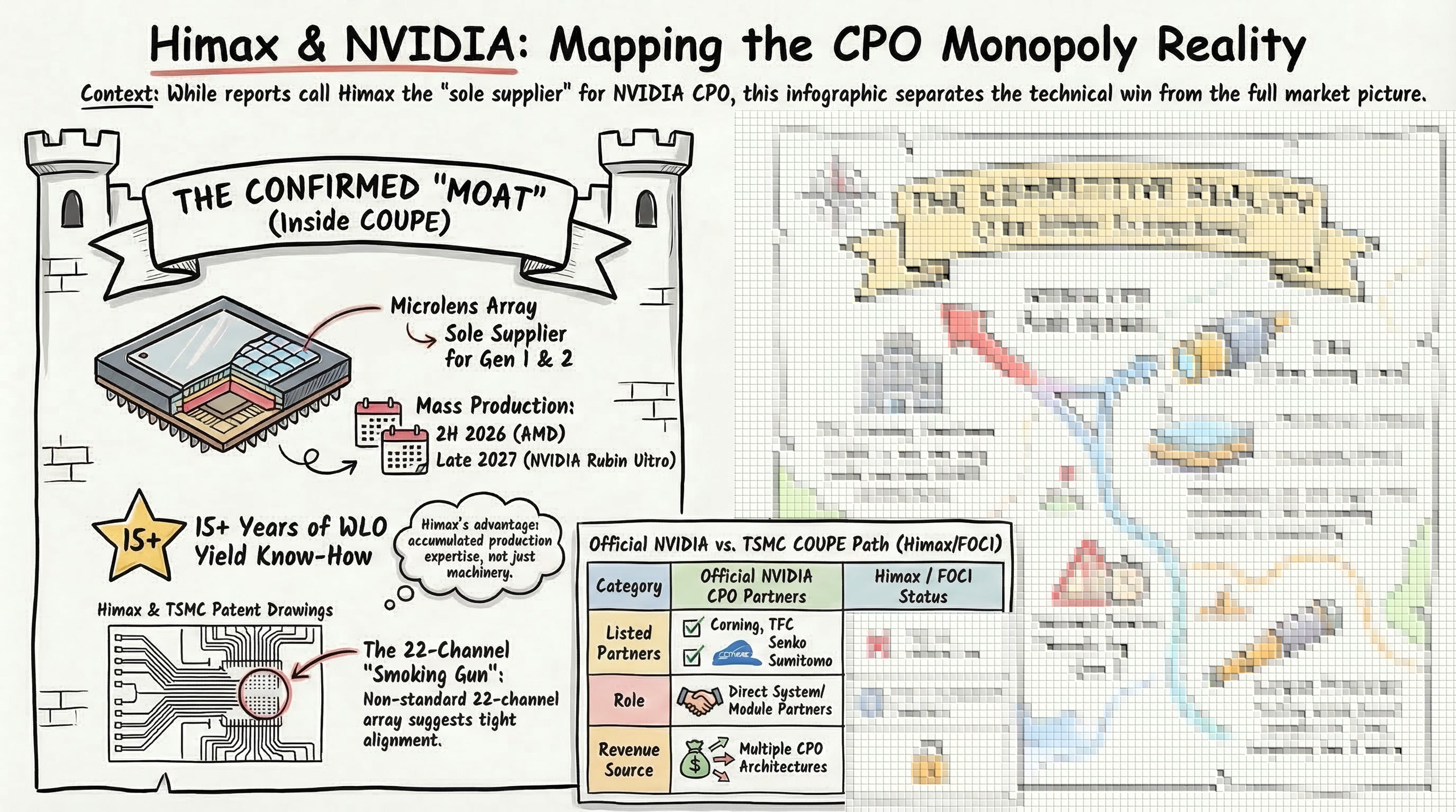
Himax manufactures the optical components inside this FAU (microlens arrays + prisms + V-groove substrates) using nanoimprint lithography (NIL). Instead of grinding lenses one at a time, NIL presses a mold into a glass wafer and stamps out hundreds of units in a single shot. Lenses on one side, 45-degree prisms on the other, all patterned simultaneously for tight alignment and high throughput. FOCI then assembles these components into finished FAUs and delivers them to TSMC [1][4].
And there is analyst confirmation backing this up. Digitimes, citing Tianfeng Securities analysts, reported that Himax is the sole microlens array supplier for both COUPE Gen 1 and Gen 2. FOCI exclusively supplies the FAUs (ReLFACon) for both generations, and a second source is unlikely before Gen 3 [18].
“Tianfeng Securities analysts noted heightened visibility for TSMC’s COUPE development, with Himax confirmed as the sole micro-lens array supplier for COUPE’s first and second generations. FOCI will exclusively supply FAUs (ReLFACon) for both generations.”
The timeline is specific. Gen 1 COUPE is scheduled for mass production in 2H 2026, with AMD as the first adopter. NVIDIA’s Rubin Ultra is likely to be the first product on Gen 2 COUPE, with production slated for late 2027 to early 2028 [18].
“The first-generation COUPE is set for mass production in the second half of 2026, with AMD poised as the initial adopter. If Nvidia’s Rubin and Rubin Ultra chips enter mass production by late 2026 and 2027, the Rubin Ultra is likely to debut TSMC’s COUPE technology.”
Bottom line: CPO is a must-have for AI data center power efficiency, and the FAU is not just bending light. It is the critical gateway for fiber-to-chip coupling (https://substack.com/@photoncap/p-190357700), connecting rack to rack, GPU to GPU. Himax being the sole microlens supplier for COUPE is real. The question is whether the scope of that monopoly is as wide as the market thinks.
1. What the Four Patents Actually Tell Us About Himax’s Technology
Hunterbrook built their case around four patents: two from Himax, one from FOCI, one from TSMC. I read all four in their original USPTO filings. (Thanks to @latent_value7 (X).)
Himax NIL Patent (US 2026/0003130 A1)
https://www.documentcloud.org/documents/27867115-himax-patent-nil-process-us-20260003130-a1/
https://www.linkedin.com/in/sam-kuo-32069b110/
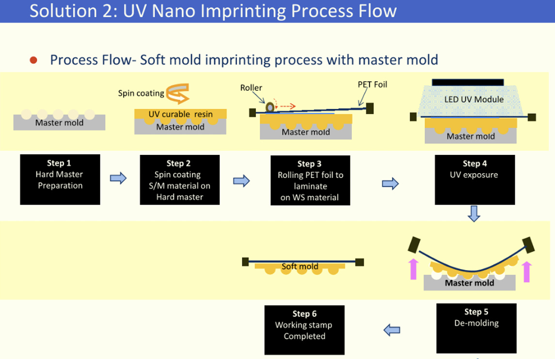
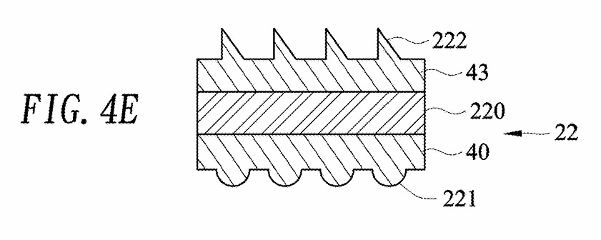
Published January 2026, this is Himax’s core claim. It is a divisional patent split from parent application 18/371,249, and as Hunterbrook correctly identified, this divisional covers the nanoimprint lithography (NIL) manufacturing process [1][4]. Specifically, it describes using NIL to stamp V-groove substrates and lens/prism components on glass wafers at the wafer level, a method well suited for high-volume production.
One thing to keep in mind here: NIL itself is not proprietary to Himax. Companies like Canon (

), EVG, and SUSS MicroTec sell NIL equipment commercially, and the process is already widely used across the semiconductor and optics industries. What sets Himax apart is not the NIL “technology” per se, but the WLO (Wafer Level Optics) production experience they have built up since the late 2000s, more than 15 years of yield know-how [5]. That accumulated production expertise is most likely the real reason they locked in the COUPE sole-supplier position.
FOCI Lens-Type Fiber Array Patent (US 2026/0036750 A1)
https://www.documentcloud.org/documents/27867114-us-20260036750-a1/
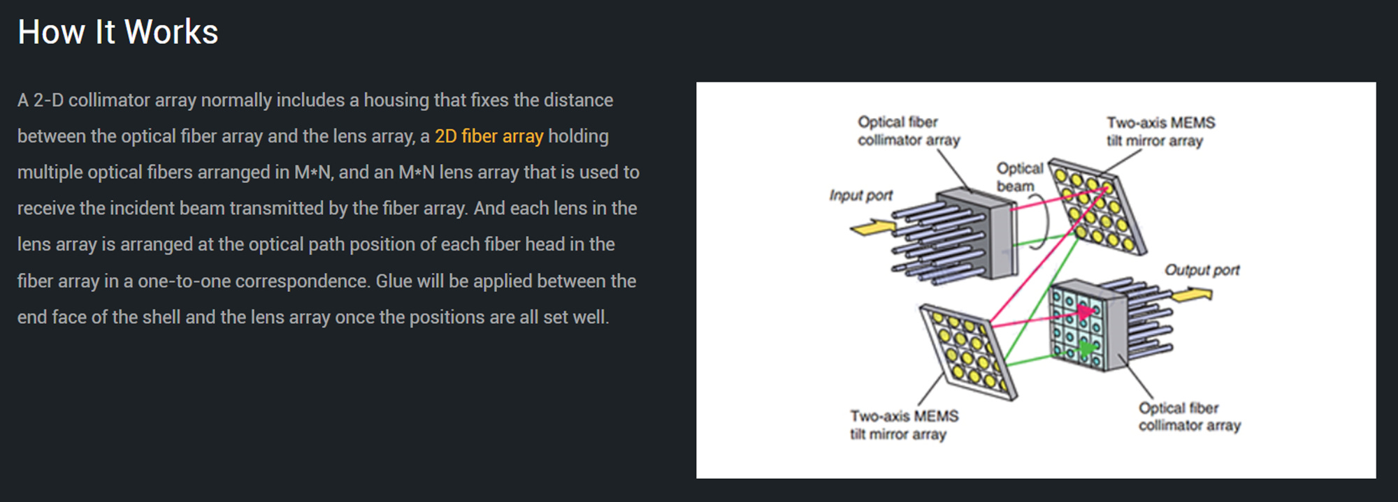
Filed by FOCI Fiber Optic Communications in October 2024 and published February 2026. This patent describes a passive alignment structure using slide rails and protruding ribs that automatically position two fiber array modules at the correct focal length [6].
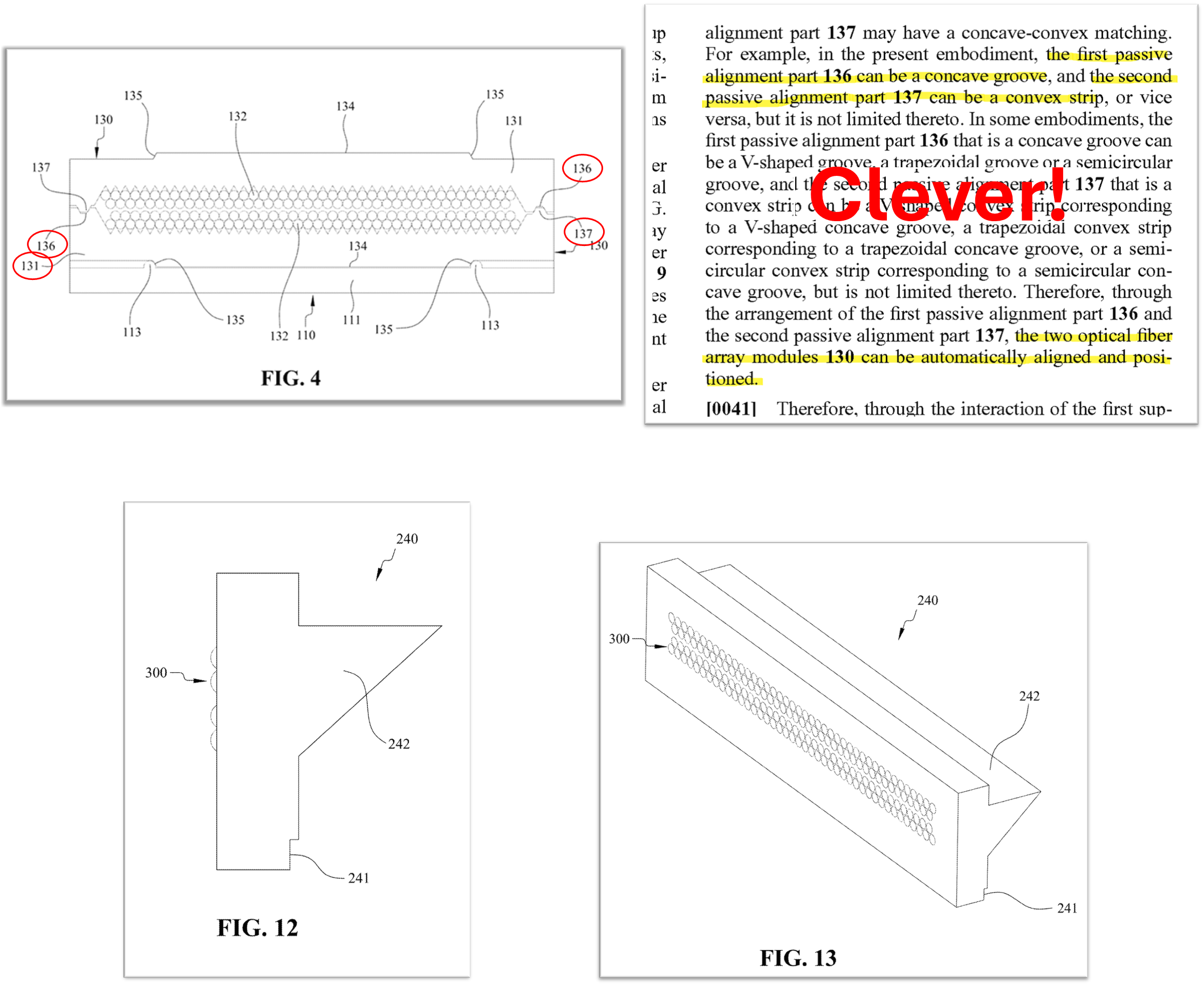
Here is what caught my eye: this patent makes zero mention of Himax. FOCI has its own independent IP covering the FAU structure. Himax supplies WLO components to FOCI, but FOCI is not structurally dependent on Himax to make FAUs.
TSMC FAU Inspection Tool Patent (US 2025/0383260 A1)
https://www.documentcloud.org/documents/27867117-tsmc-patent-inspection-tool-us-2025383260-a1/
This one was personally the most interesting to me. Filed by TSMC in June 2024 and published December 2025, it describes a 5-mode integrated inspection system specifically for FAU quality control in CPO applications [7].
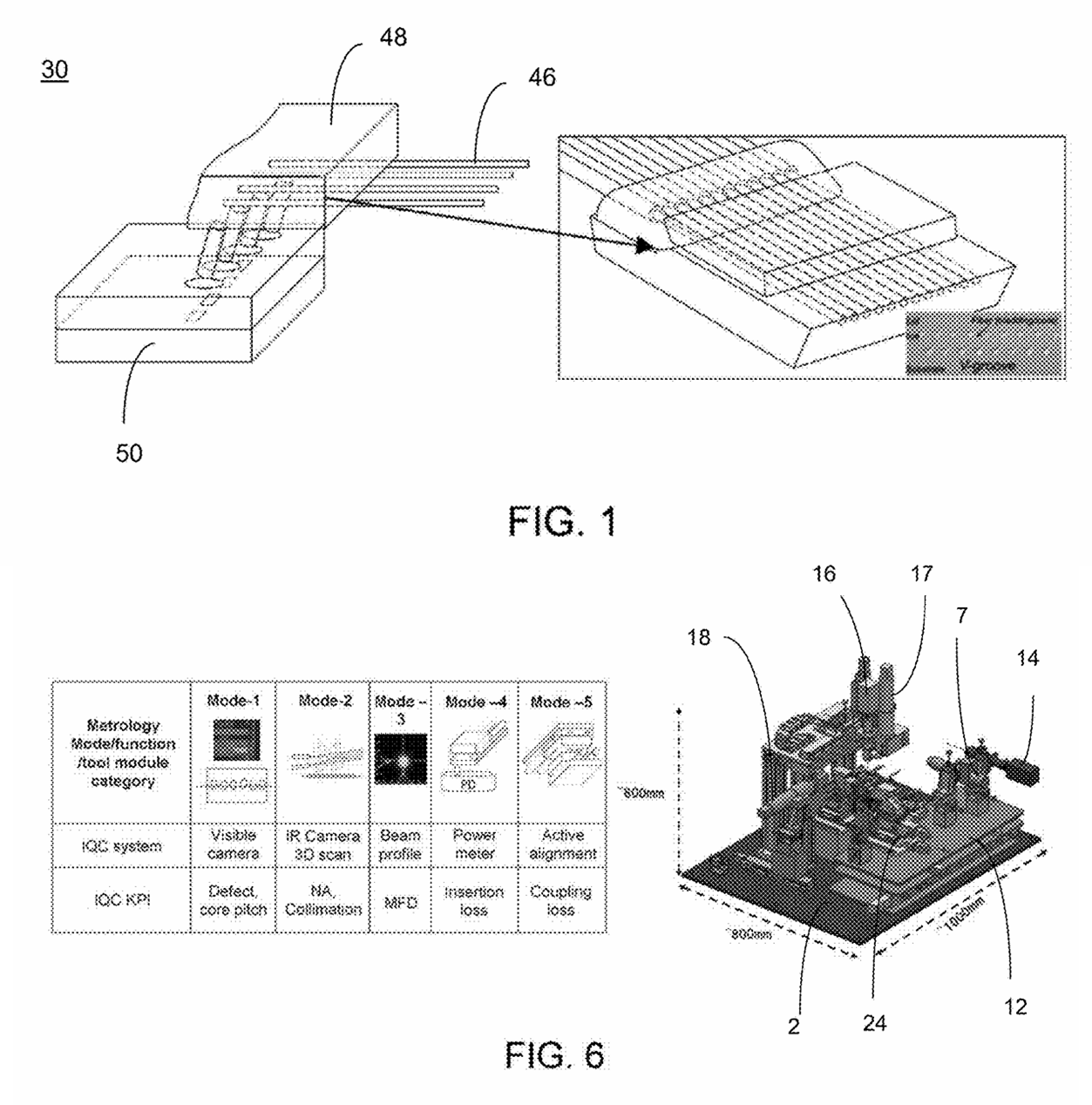
The five inspection modes are: (1) visible camera for defect/pitch detection, (2) IR camera for 3D core pitch scanning, (3) beam profiler for MFD (Mode Field Diameter) measurement, (4) power meter for insertion loss, and (5) active alignment against a golden FAU reference.
Why does this matter? Because TSMC is building its own verification infrastructure for externally sourced FAUs. No specific supplier is named anywhere in the patent. The system is designed to accept FAUs from any supplier that meets spec. This is the opposite direction from single-supplier lock-in.
Hsia, Harry, et al. “EPIC-BOE: An electronic-photonic chiplet integration technology with IC processes for broadband optical engine applications.” 2024 IEEE International Electron Devices Meeting (IEDM). IEEE, 2024.
Hunterbrook pointed out that the FAU schematic in TSMC’s patent matches the Himax FAU structure. That is correct. But the vertical coupling FAU design (prism bending light 90 degrees into horizontal fibers) is an industry-standard architecture, not something unique to Himax [19].
Take, for example, Chinese company Meisu (https://www.meisuoptics.com/products/2d-fiber-arrays-assemblies/), which already manufactures 2D collimator arrays and 2D fiber arrays [21].
The 22-Channel “Smoking Gun”
Hunterbrook’s strongest circumstantial argument: the Himax patent shows exactly 22 lenses in its array diagram, and the TSMC inspection patent depicts 22 channels (ch1 through ch22). In the fiber optics world, 22 is a non-standard number (standard counts are 12, 16, 24, 32, 48, 64). This suggests both patents are describing the same component [1].
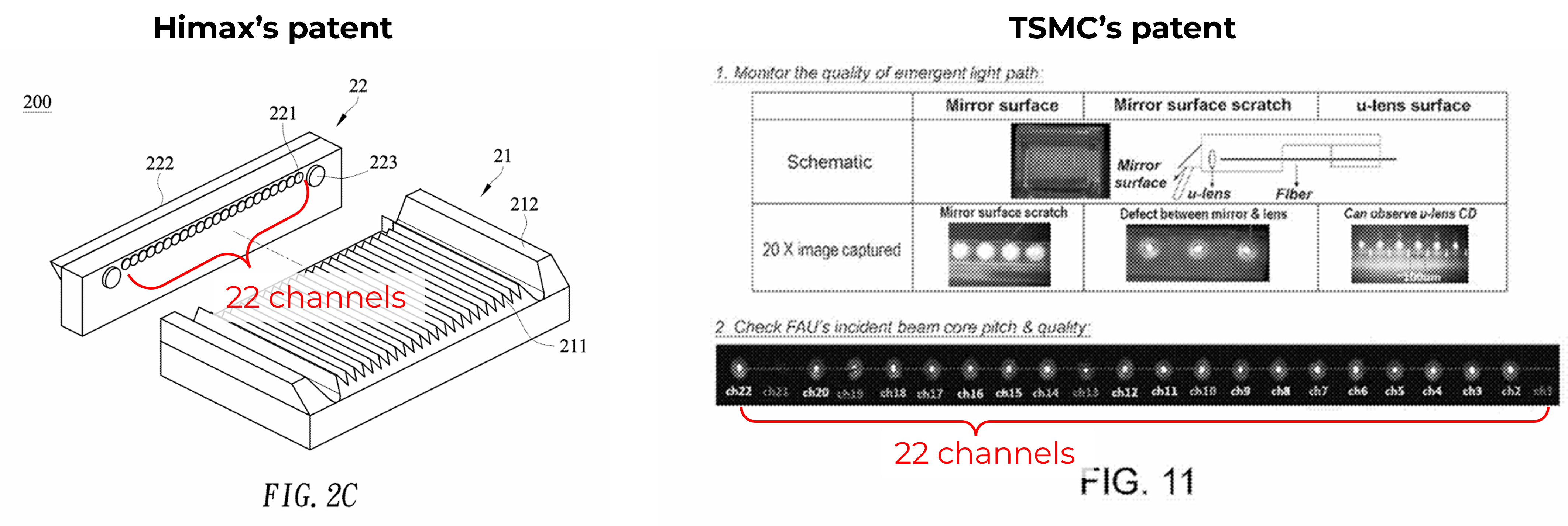
It is an interesting observation, and I personally give it high marks. But patent drawings use illustrative numbers. According to Hunterbrook, a separate Himax prism testing patent (TW I896409 B) explicitly states “16, 22, or 50 lenses, but the number is not limited thereto” [1]. The 22-channel overlap across multiple patents is worth noting, but it falls short of definitive proof.
Bottom line: Himax’s NIL production experience is a real capability backing their COUPE microlens monopoly. But NIL itself is a widely available process, TSMC’s inspection patent signals a structure that allows for long-term supplier diversification, and FOCI holds independent FAU-structure IP separate from Himax.
