
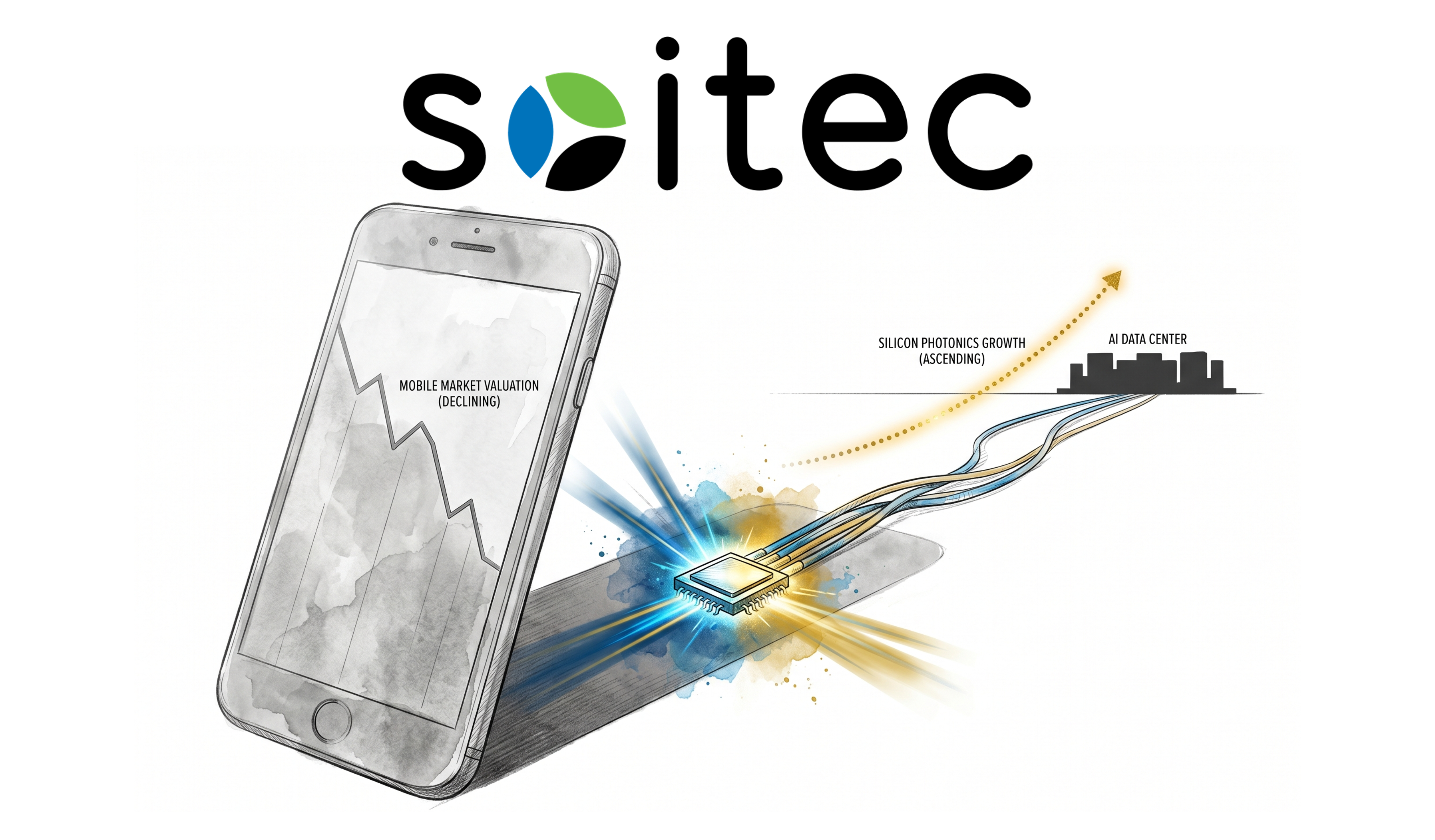
The Wafer That Used to Roll Around My Lab Is Now an AI Data Center Bottleneck: Soitec and the Investment Case for the Photonics-SOI Monopoly
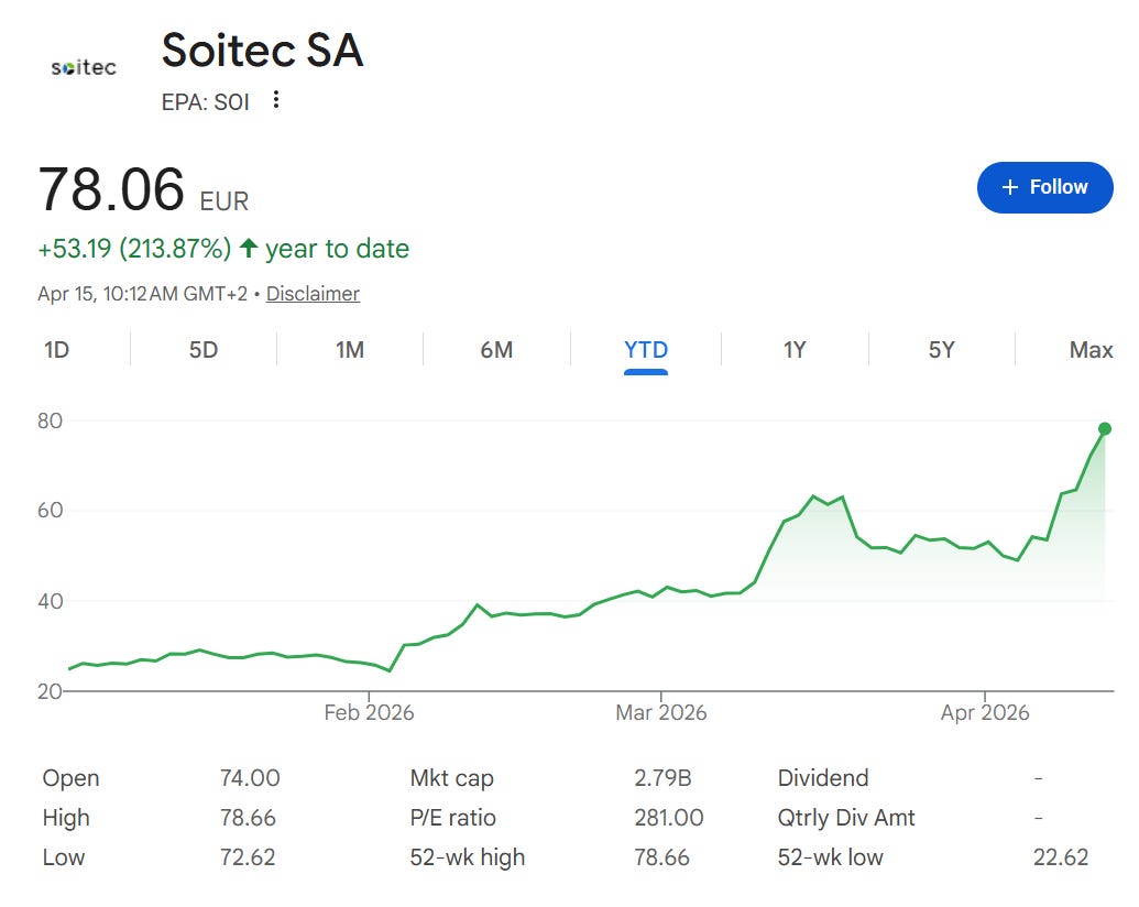
As AI data centers accelerate the transition from electrical to optical interconnects, demand for SOI (Silicon-on-Insulator) wafers, the critical substrate for silicon photonics (SiPh), is growing rapidly. This article analyzes Soitec’s (EPA: SOI) technological moat (3,500+ Smart Cut patents, no competitor with meaningful Photonics-SOI volume identified from public sources), financial profile (FY2025 revenue of €891M, Photonics-SOI approaching €100M scale), and the reality behind the SiN platform threat narrative. Soitec’s stock rallied from its December 2025 low of €23 to €78 as of April 15, 2026, a YTD gain of +213%, as the market began pricing in its SiPh/CPO positioning. But the actual Photonics-SOI revenue scale-up is still in its early innings. The real test comes over the next 2 to 3 years as 1.6T/CPO ramps accelerate. Related tickers: $SOI (EPA), $SLOIF (OTC), $GFS, $TSEM
Contents
Intro: From Lab Bench Wafer to AI Infrastructure Chokepoint
What Is an SOI Wafer?
Soitec’s Moat: The Smart Cut Monopoly
The SiN Threat: Real or Overstated?
Financials: Photonics-SOI Growth Inside a Mobile Downcycle (paid)
Competitive Landscape and the China Question (paid)
CEO Transition, Singapore Expansion, and Market Tailwinds (paid)
Scenario Analysis + Investment Implications (paid)
Closing
References & Sources
1. Intro: From Lab Bench Wafer to AI Infrastructure Chokepoint
Soitec’s stock went from €23 in December 2025 to €78 as of April 15, 2026. That is +213% year-to-date, currently printing new 52-week highs at €78.66. The market has finally woken up to this company’s silicon photonics positioning.
Back in 2017, when I was finishing my master’s degree, SOI wafers were just things lying around the lab. I was on the photonics side, and SOI was the default substrate for waveguide experiments. The RF guys in the same lab used SOI too. Soitec wafers were so standard that I never thought twice about the company behind them.
The situation is different now. The stock had been falling because of RF-SOI (smartphones) inventory correction, but the reason SOI is becoming important again is something entirely different: silicon photonics. The market recognized this, and the recent rally followed.
But the question has changed. Is this rally justified? And is there still more to come?
Soitec owns the Smart Cut patent technology that gives it a dominant position across the SOI ecosystem, and in Photonics-SOI, the substrate for AI optical interconnects, no competitor with meaningful production volume has been identified from public sources. Even Shin-Etsu, the world’s largest silicon wafer maker, licenses Soitec’s technology to produce SOI wafers.[1] Management has said Photonics-SOI revenue is approaching €100M scale, but the real capacity ramp at Tower and GFS is just starting now. Our view is that the actual Photonics-SOI scale-up is still in its early innings.
This article covers the technical structure of SOI wafers, why Soitec’s dominant position is so hard to challenge, whether SiN (silicon nitride) is a real competitive threat, and whether the photonics growth runway still extends well beyond the recent rally.
Key takeaway: The market has started to recognize Soitec’s SiPh positioning, but the actual Photonics-SOI revenue scale-up is still in its early innings. The next 2 to 3 years, as 1.6T/CPO ramps accelerate, are the real proving ground.
2. What Is an SOI Wafer?
To understand SOI, you need to know what makes it different from a regular silicon wafer.
A standard silicon wafer is a single chunk of monocrystalline silicon. TSMC and Samsung Foundry etch transistors on top of it. An SOI wafer, as the name says, is “Silicon on Insulator.” Think of it as a sandwich. On top, a very thin silicon layer (the device layer). In the middle, an oxide insulating layer (BOX, or Buried Oxide). On the bottom, a thick silicon support (the handle wafer). That middle insulating layer blocks electrical interference between the device layer and the substrate.[2]
Here is a simple analogy. A regular wafer is like laying wires directly on the ground. An SOI wafer is like laying wires on an insulating mat. Signal leakage goes down, and parasitic capacitance (unwanted electrical coupling between components) drops significantly. For a deeper look at SOI wafer structure and silicon waveguide physics, see our previous article.[32]
[PC101] Lecture 2: Standing on the Shoulders of Giants — CMOS Process Leverage and Economic Moat
![[PC101] Lecture 2: Standing on the Shoulders of Giants — CMOS Process Leverage and Economic Moat](https://substackcdn.com/image/fetch/$s_!76sU!,w_1300,h_650,c_fill,f_webp,q_auto:good,fl_progressive:steep,g_auto/https%3A%2F%2Fsubstack-post-media.s3.amazonaws.com%2Fpublic%2Fimages%2Fd08a3507-0529-4d21-9185-a83451cbc142_2046x819.jpeg)
“If I have seen further it is by standing on the shoulders of giants”
This structure gives rise to several SOI product variants, each tuned for different applications.
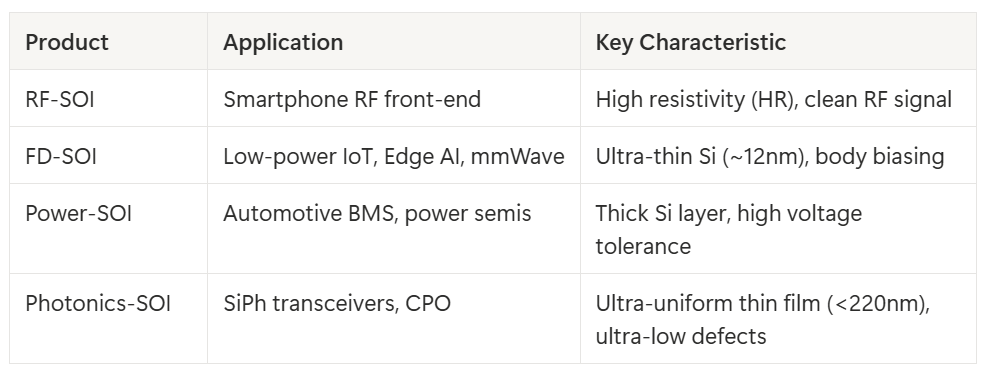
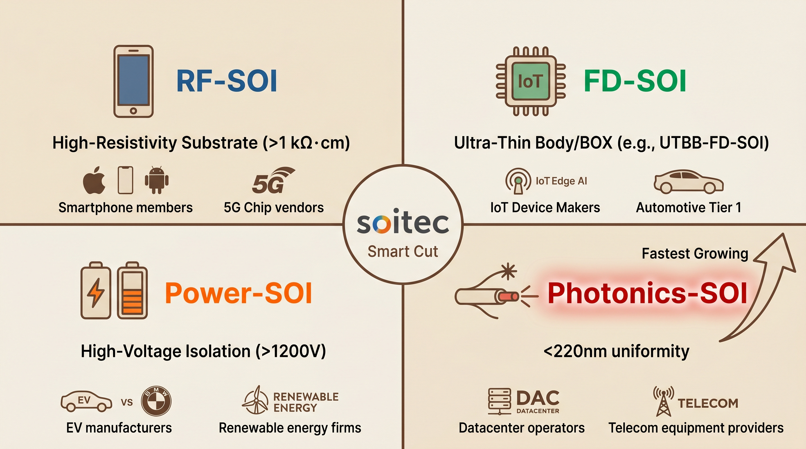
Soitec SOI Wafer Product Portfolio Map
The important point here is not the technology itself. It is the manufacturing. SOI wafers are more expensive than standard bulk silicon wafers because inserting that middle insulating layer is a difficult process. And there is exactly one technology that can do this efficiently at scale.
SOI wafers are a “silicon on insulator” sandwich structure. More expensive than standard wafers, but irreplaceable for RF and photonics performance.
3. Soitec’s Moat: The Smart Cut Monopoly
That technology is Smart Cut.
Smart Cut was invented in the early 1990s by Michel Bruel at CEA-Leti, a French national research lab. The basic principle works like this. You implant hydrogen ions into a donor wafer. You bond this wafer face-to-face with an oxidized handle wafer using molecular adhesion bonding. Then you apply heat. The silicon cleaves precisely at the depth where the hydrogen was implanted. The result is a nanometer-precision ultra-thin silicon film transferred onto an insulator.[3]
Think of it as slicing a sheet of paper to an exact thickness and transferring it onto another surface, except you are doing this at atomic-level precision. Across an entire 300mm wafer, the thickness variation has to stay within a few angstroms.
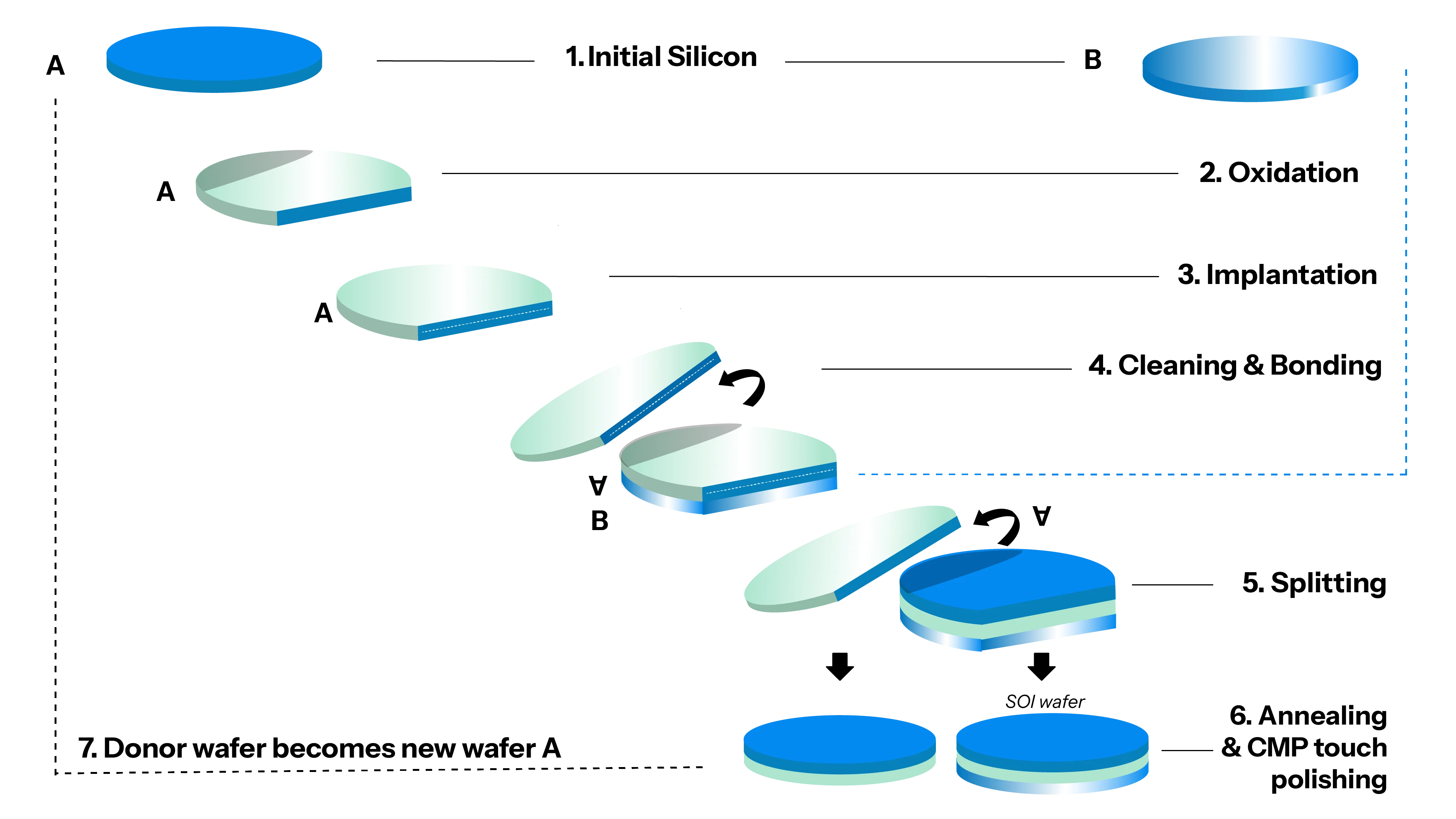
The Smart Cut process in action can be seen in this video.
There are other ways to make SOI wafers. SIMOX (Separation by Implanted Oxygen) creates the insulating layer by implanting oxygen ions directly into silicon. But SIMOX requires expensive equipment and is more complex, making it uneconomical for high-volume manufacturing. Smart Cut is cheaper and produces better quality, so the market converged on Smart Cut.
This is where Soitec’s moat forms.
Soitec holds the exclusive license to CEA-Leti’s Smart Cut technology. The company controls over 3,500 related patents. Any competitor that wants to use this technology has to pay Soitec a licensing fee.[4]
Shin-Etsu Handotai (SEH), the world’s largest silicon wafer producer, has been licensing Smart Cut from Soitec since 1997. This license was extended for another 10 years in 2012 and expanded into a cross-licensing arrangement.[5] GlobalWafers does the same.
Economically, this matters because Soitec captures either product revenue or royalty revenue across much of the SOI ecosystem. It earns sales revenue on wafers it produces directly, and royalties on wafers produced by licensees. About 80% of the SOI market runs on Smart Cut, and Soitec captures value from most of it.[6]
In Photonics-SOI, this dominance gets even stronger.
Photonics-SOI has far more demanding specifications than standard RF-SOI. In silicon photonics, light propagates through the top silicon layer of the SOI wafer, which acts as a waveguide. This waveguide is typically under 220nm thick, and the thickness variation across the entire wafer has to be extremely small. If it is not, the optical phase drifts, and modulator and ring resonator performance collapses.
RF-SOI tolerates thickness uniformity in the range of a few nanometers. Photonics-SOI requires an order of magnitude better. Surface defect density has to be extremely low as well. From public sources, Soitec is the only photonics-grade SOI supplier clearly documented at meaningful 300mm scale.[7]
The industry consensus is that Soitec holds a dominant position in the photonics-grade SOI market.[8] Shin-Etsu and GlobalWafers have Smart Cut licenses, but neither has meaningful Photonics-SOI revenue.
If TSMC is the dominant player in cutting-edge logic, Soitec holds a comparable position in the specialty wafer that TSMC’s SiPh customers need. The difference is that TSMC’s moat comes from trillions of dollars in cumulative capex. Soitec’s moat comes from patents and know-how.
Soitec is the exclusive licensor of Smart Cut technology, capturing value across the entire SOI wafer market. In Photonics-SOI, no competitor with meaningful volume production has been confirmed.
4. The SiN Threat: Real or Overstated?
Whenever you talk about the future of SOI, one question always comes up. “Won’t silicon nitride (SiN) replace SOI?”
SiN has been studied since the 1970s and is already widely used in CMOS processes for isolation trenches and passivation (surface protection). When researchers discovered it also has useful photonic properties, it started being discussed as an alternative to SOI.[9]
SiN has real advantages. First, its propagation loss is much lower than SOI. SOI losses are measured in dB/cm. SiN losses can reach dB/m, a thousand-fold improvement. Second, its transparency window is broader, covering visible light (~400nm) all the way to near-infrared (~2,350nm). SOI only works above about 1,100nm.[10] Third, SiN is CMOS-compatible, just like SOI.
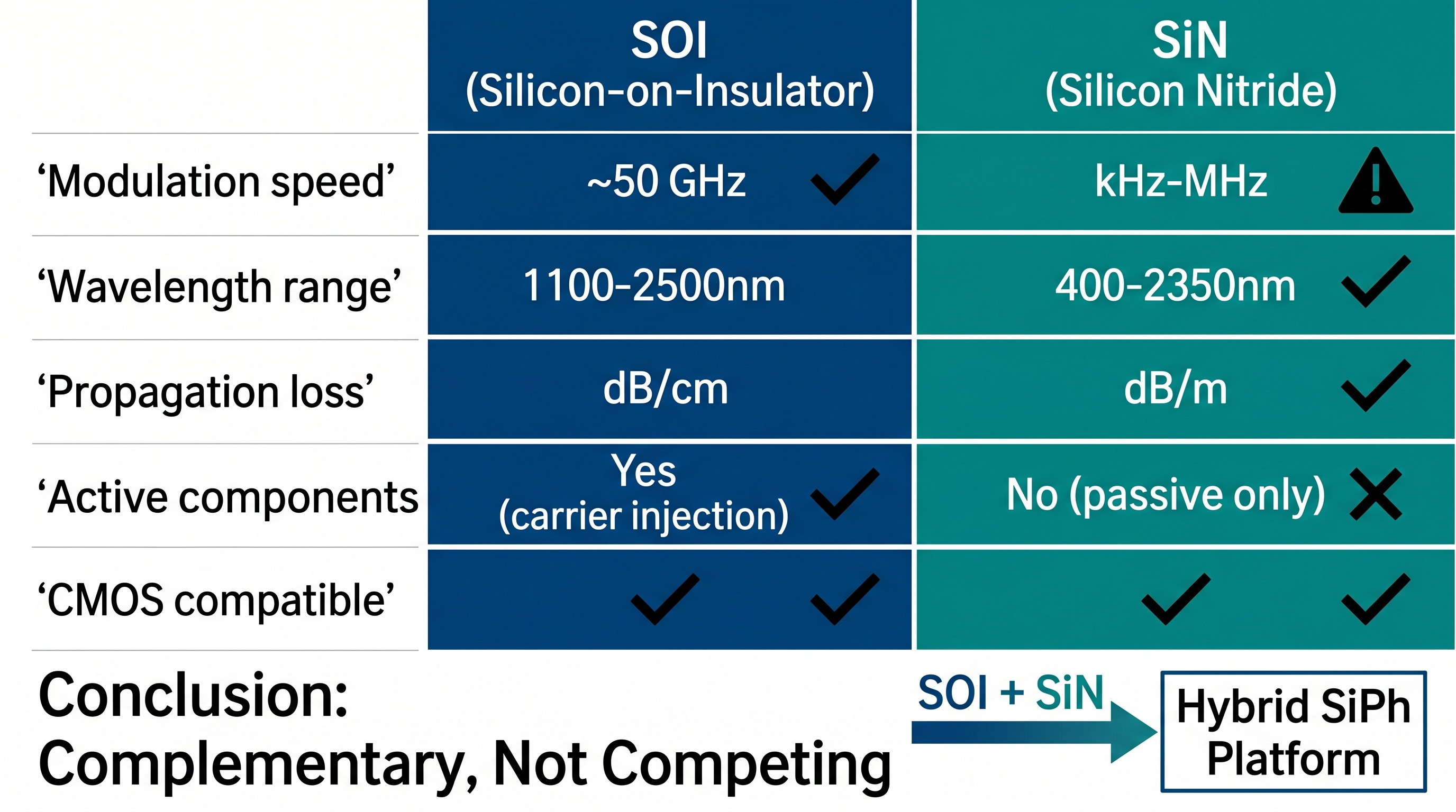
SOI vs SiN Platform Comparison
So will SiN replace SOI? In the context of data center SiPh, that claim is overstated.
SiN is a passive material. It cannot generate light on its own, and it cannot modulate light at high speeds. Thermal-based modulation tops out in the kHz range. Piezo-assisted switching reaches a few hundred MHz at best. Data center transceivers need modulation speeds in the tens of GHz. SiN alone cannot get anywhere close to that.[11]
SOI, on the other hand, enables electro-optic modulation at tens of GHz through carrier injection and depletion in silicon. Germanium photodetectors can be directly integrated on SOI as well.
So what are the actual SiPh foundries doing? They use both. Tower Semiconductor’s PH18 platform, GlobalFoundries’ Fotonix platform, and IMEC’s iSiPP platform are all SOI-based with SiN waveguide layers added on top.[12] SiN is entering as a complement to SOI, not a replacement.
In my reading, as SiN layers get added, the specifications for the underlying SOI wafer become more demanding, not less. Stacking multiple precision layers on top of each other requires an even more uniform and defect-free starting substrate.
But the technology moat alone does not make an investment case. The real question is not whether Soitec is a good company. It is whether Photonics-SOI can become a “too big to ignore” revenue line before the mobile inventory correction finishes. And the answer to that question lies not in the technology, but in customer expansion timelines and fab utilization leverage.
In the current data center SiPh ecosystem, SiN is being adopted as a complementary layer within SOI-based platforms, not as a standalone replacement. SiPh foundries are building hybrid SOI + SiN platforms, which raises, not lowers, the quality bar for the underlying SOI wafer.
