
[PC101] Lecture 4:The Last Millimeter: Fiber-to-Chip Coupling and the CPO Packaging Bottleneck (Part 1)
— Coupler design principles and trade-offs for bridging the 1,000× mode mismatch —

Welcome back. This is PhotonCap.
In Lecture 3, we laid down the roads for light inside the chip (waveguides), installed traffic lights at intersections to split and combine beams (splitters, couplers), and placed roundabouts that filter specific colors of light (ring resonators). The on-chip traffic infrastructure is in place.
[PC101] Lecture 3: Traffic Control for Light: Waveguides and Passive Devices
![[PC101] Lecture 3: Traffic Control for Light: Waveguides and Passive Devices](https://substackcdn.com/image/fetch/$s_!hX_j!,w_280,h_280,c_fill,f_webp,q_auto:good,fl_progressive:steep,g_auto/https%3A%2F%2Fsubstack-post-media.s3.amazonaws.com%2Fpublic%2Fimages%2Fd4a25ec4-43ac-426b-b3f2-7a63460bc663_5300x2739.png)
“The devil is in the details.”
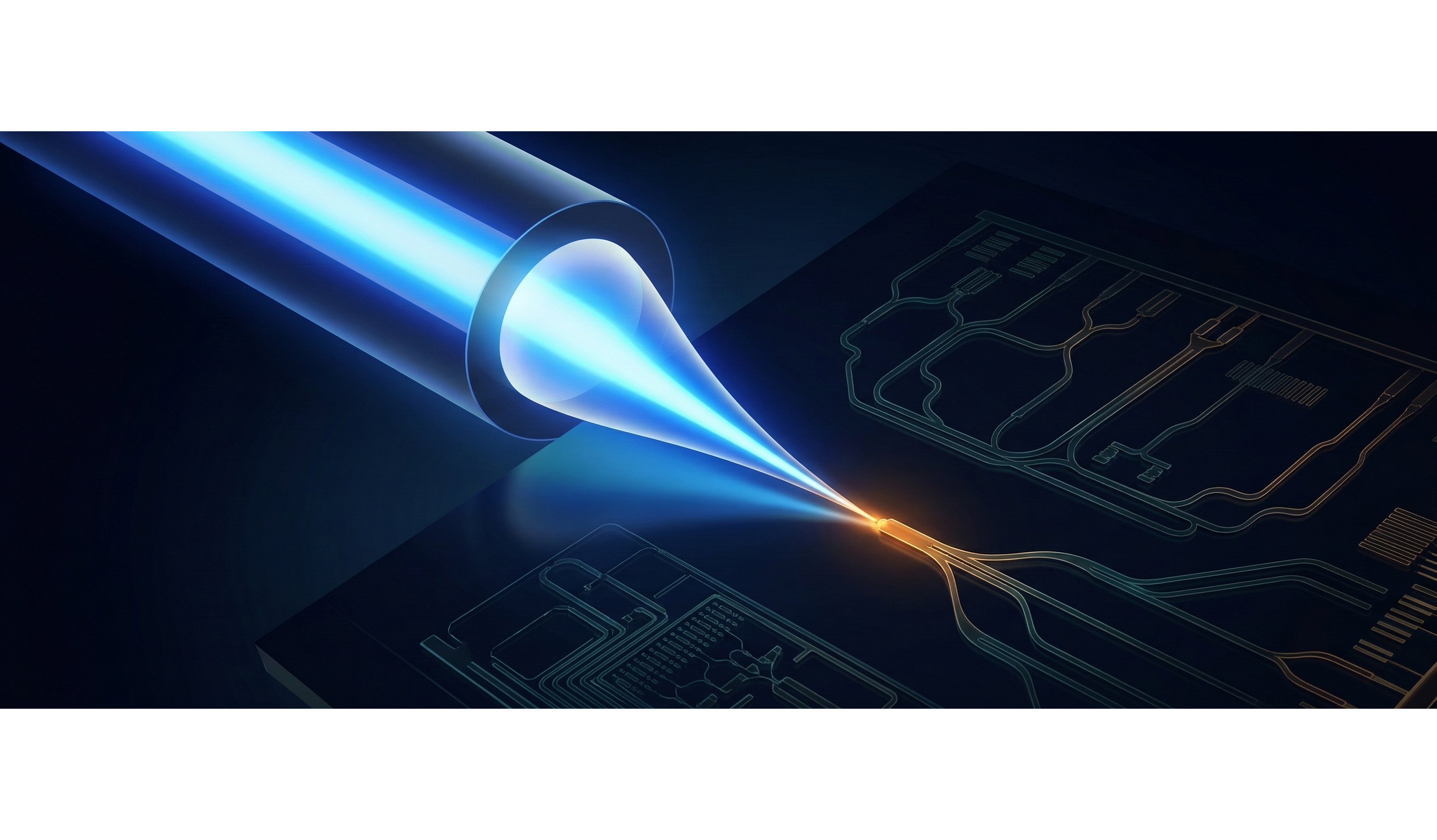
But one thing is missing — the highway on-ramp. No matter how well the roads inside the chip are built, they’re useless if light from the outside world (optical fiber) can’t get in. The problem? The highway is 1,000 times wider than the city’s alleyways.
Lecture 4 tackles this “last millimeter” challenge, covering six coupling technologies — including those already adopted by industry and others still emerging from research.
1. Introduction: Why ‘Packaging’ Is the Biggest Bottleneck in Silicon Photonics
Modern data communication and high-performance computing architectures face unprecedented demands for bandwidth expansion, driven by the explosive growth of AI, cloud, and ultra-high-resolution streaming. Traditional copper (Cu)-based electronic packaging causes significant power loss and signal integrity degradation at centimeter-scale board-level transmission, serving as a physical limit on switch package bandwidth scaling. According to SemiAnalysis, optical transceivers alone consume approximately 17 MW in a 200,000-GPU-scale GB300 NVL72 cluster. CEO Jensen Huang also emphasized at GTC 2025 that scaling to one million GPUs would require 6 million transceivers consuming tens to hundreds of megawatts, underscoring the necessity of Co-Packaged Optics (CPO) [1].
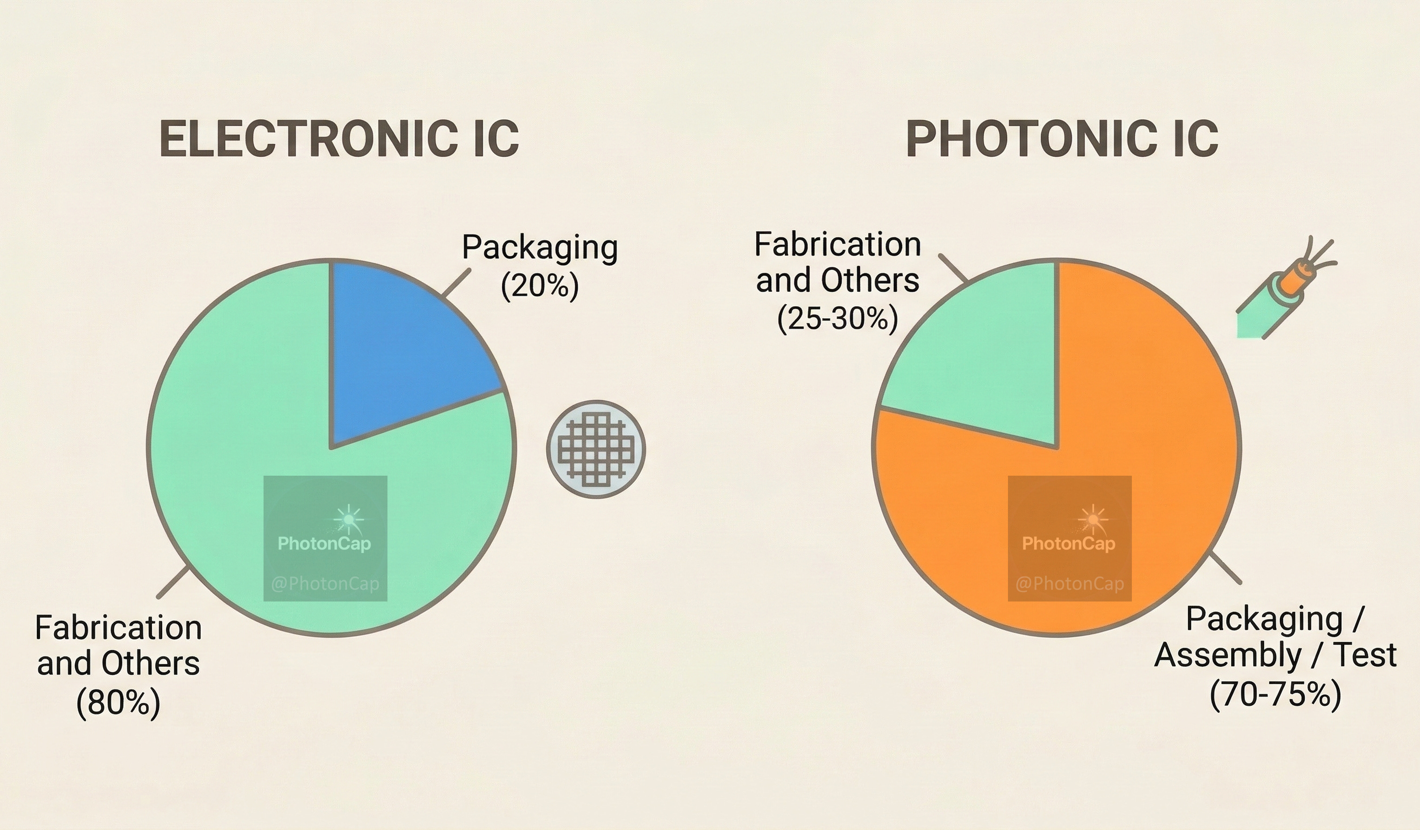
Silicon photonics-based Photonic Integrated Circuits (PICs) have emerged as a key alternative to overcome this electronic bottleneck. Although manufacturing technology capable of integrating 10³–10⁵ optical devices on a single die has already matured, the photonics industry faces another severe bottleneck: Packaging, Assembly, and Test [2][3].
For electronic ICs, packaging accounts for roughly 20% of total manufacturing cost, whereas for silicon-based PICs this figure reaches 70–80%—a strikingly disproportionate structure [2][3][4]. Specifically, while cutting-edge 5 nm electronic SoCs cost approximately $0.57/mm² before packaging, silicon photonic chips cost only $0.1–0.4/mm² for the die itself [2]. Yet the final module cost escalates dramatically due to the physical difficulty of optical alignment and resulting assembly throughput limitations. While electronic packaging has evolved to large-scale passive alignment processes using solder bumps and hybrid bonding, photonic packaging still heavily relies on active alignment—directly injecting light to find the optimal coupling position [3][4].
This article (Part 1 of 2) analyzes the physical principles and structural limitations of optical I/O coupling technologies connecting chip interiors and exteriors, and compares the design metrics and trade-offs of major couplers (Edge, Grating, Evanescent, Free-form, Cantilever, Photonic Wirebond). Part 2 covers 3D Photonic Vias technology, CPO, quantum photonics, LiDAR, and other next-generation system applications
Why Optical Coupling Is the Bottleneck in System Evolution
The figure below illustrates how the position and requirements of the fiber-chip coupling interface change as datacenter switch architecture evolves from Pluggable Optics to 3D CPO [13].
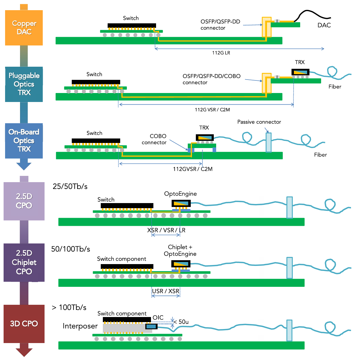
The key point at each stage is where the fiber couples to the package. In the Pluggable approach, approximately 25 cm (~10 inches) of long electrical traces span across the PCB between the ASIC and transceiver (OE), with fibers coupling at the board edge using off-the-shelf connectors with relaxed tolerances (±10 µm). In 2.5D CPO, the optical engine sits on the same package substrate as the ASIC, reducing the electrical path to ~5 mm, with fibers coupling directly to the PIC at the package edge. In the final stage—3D CPO—the PIC is stacked directly above the ASIC on an interposer with electrical paths under 50 µm, making the fiber-to-chip coupling interface the single most critical point determining package performance and cost.
In other words, as integration tightens, the requirements for fiber-to-chip (F2C) coupling technology fundamentally change. In the Pluggable era, 2–3 dB of coupling loss was acceptable with generous connector tolerances, but in 3D CPO, thousands of channels must be coupled simultaneously at sub-dB loss with passive alignment.
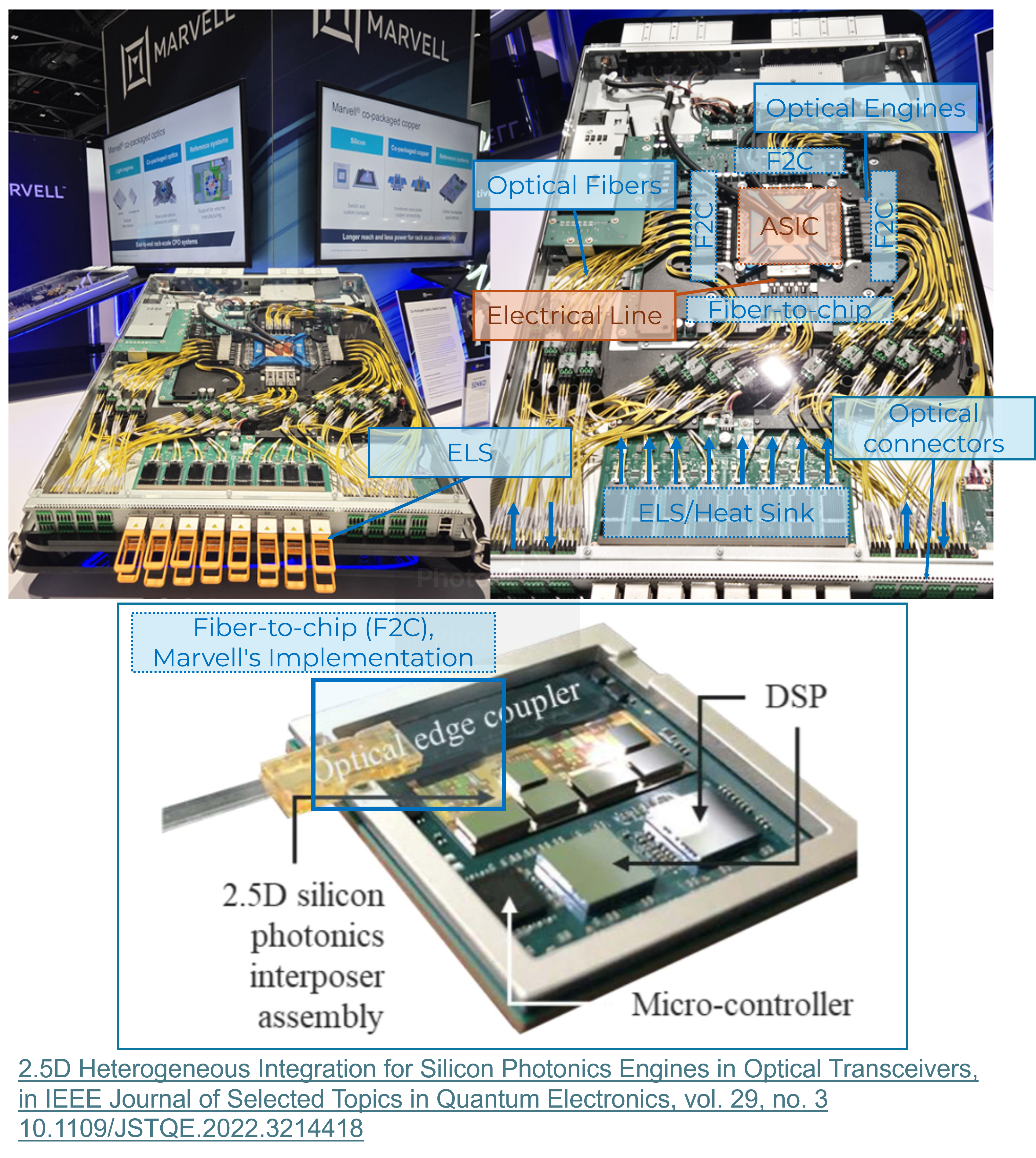
The photo above shows the internals of the TX9190, a 51.2 Tbps liquid-cooled CPO switch jointly unveiled by Marvell and Jabil at OCP Summit 2025. Surrounding the ASIC are numerous optical engines connected by hundreds of fiber strands. Each optical engine contains a fiber-to-chip (F2C) coupling interface where the PIC waveguide meets the optical fiber.
One example of an F2C approach is the edge coupler. (The specific F2C method used in the TX9190 CPO switch will be covered in Part 2.) As CPO architectures evolve, the number of optical engines per package and channel density both increase, which inevitably drives up the number of these F2C assemblies. This is the fundamental reason why optical packaging technology is becoming exponentially more important. The coupling techniques covered in Part 1 (edge, grating, evanescent, free-form, and PWB) each address different stages and interface requirements along this roadmap. Understanding the insertion loss, alignment tolerance, and bandwidth tradeoffs of each is the starting point for CPO system design.
2. Physical Principles of Optical Coupling: The 1,000× Mode Mismatch
Coupling efficiency is the ratio of optical power transferred between two different optical waveguides, fundamentally determined by the spatial overlap of Mode-Field Diameter (MFD) and reflectance due to refractive index mismatch [2][5].
At the telecommunications wavelength (1550 nm), standard single-mode fiber (SMF-28) has a core diameter of approximately 8.2 µm and MFD of approximately 10.4 µm [6]. In contrast, a silicon waveguide (refractive index ~3.45) embedded in silica cladding (~1.45) operating in single-mode condition has a cross-section of approximately 400 nm × 220 nm, confining the optical mode to approximately 0.1 µm² [5]. The cross-sectional area difference between these two media is approximately 1,000×—the most fundamental physical barrier to high-efficiency optical coupling.
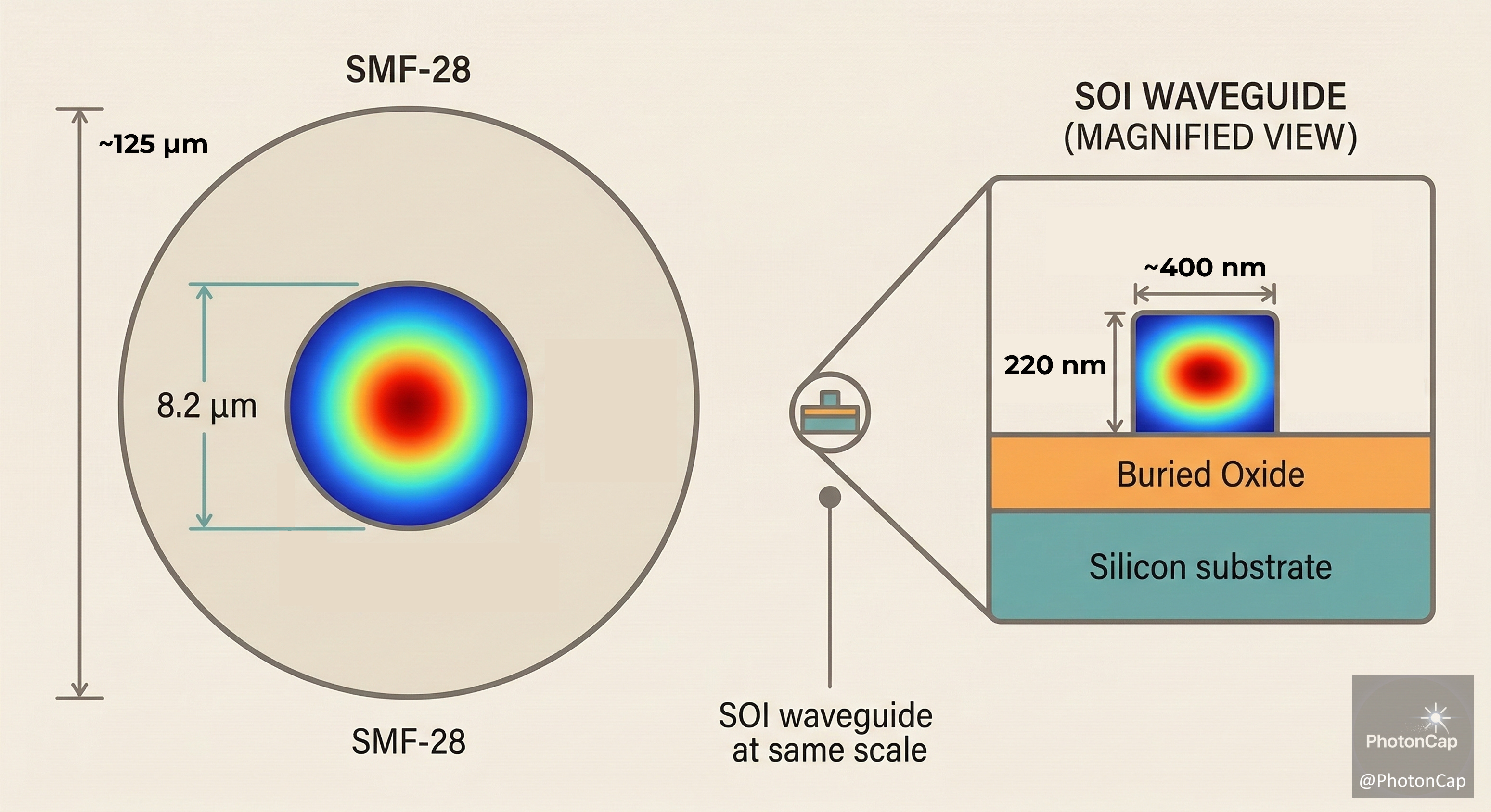
💡 [Analogy: Connecting a fire hose to a nano-straw]
Imagine feeding the water stream from a 10 cm diameter fire hose (optical fiber) into a 0.5 cm straw (chip waveguide) without spilling a drop. The cross-sectional area differs by approximately 1,000×, requiring specialized structures to physically transform the spatial shape (mode) of light.
Given the electric field distribution of the input waveguide E₁(r, φ) and the output waveguide E₂,ₖ(r, φ), the coupling efficiency ηₖ into the k-th guided mode is derived from the overlap integral [5]:
This expression shows that mode size mismatch (w₁/w₂) and lateral, longitudinal, and vertical alignment errors exponentially degrade coupling efficiency. Numerical analysis indicates that mode size mismatch has a more dominant effect on coupling loss than alignment error [5].
Additionally, the difference in effective refractive index (n_eff) between the two media causes Fresnel reflection at the interface. The transmission coefficient is t₂ = 2(n_eff,1 · n_eff,2)⁰·⁵ / (n_eff,1 + n_eff,2), so the total coupling efficiency is |t₂|² · ηₖ. Here |t₂|² = 4n₁n₂/(n₁+n₂)² is the power transmittance (T) at the interface, following the notation of [5]. Therefore, the design goal of all optical couplers is to maximize ηₖ through gradual geometric deformation that expands/contracts the MFD, and to control refractive index to bring |t₂|² close to 1 [2][5].
3. Edge Coupling: Intuitive but Demanding
3.1. Inverse Tapers and Spot-Size Converters (SSC)
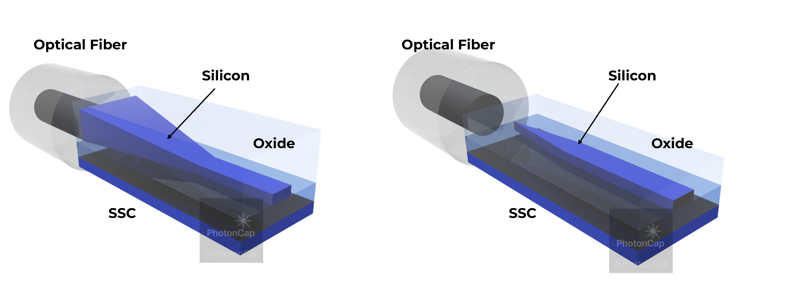
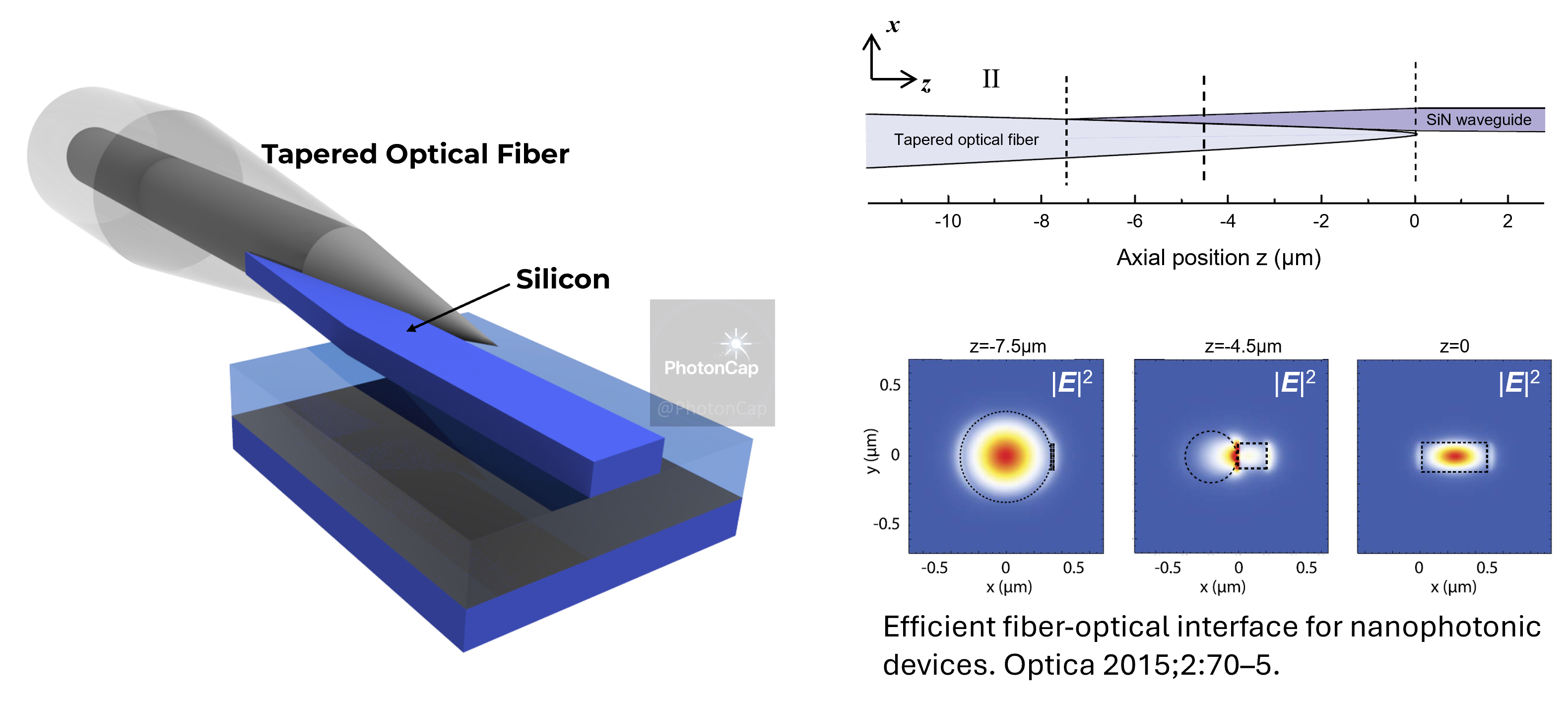
Edge coupling (end-fire or butt coupling) is the most intuitive approach, directly facing the physical cross-sections of waveguides to transfer optical signals. A spot-size converter (SSC) is essential to resolve the mode mismatch on the high-index silicon photonics platform [5][7].
The most intuitive approach is 3D tapering of the silicon waveguide in both horizontal and vertical directions to directly expand the PIC mode to fiber mode size. However, this is not widely adopted in production lines due to the process complexity requiring multi-step etching or grayscale lithography in the vertical direction. Instead, the most widely used structure is the inverse taper, which gradually narrows the silicon waveguide width to tens to hundreds of nanometers (e.g., 100–200 nm) toward the chip edge. As the waveguide core narrows, the optical mode confinement weakens and the electromagnetic field expands in the form of an evanescent field, reducing the effective refractive index. Wrapping this with low- or medium-index 2D/3D overlay waveguides made of polymer, SiO₂, SiON, or Si₃N₄ ultimately forms an MFD of 3–10 µm diameter, enabling efficient coupling with lensed fiber, UHNA (Ultra-High Numerical Aperture), or standard SMF-28 fiber [5][7].
💡 [Analogy: Mist spreading from a needle tip]
In the wave world of light, when a silicon waveguide tip is shaved below 100 nm, the light can no longer be confined in the narrow silicon and spreads outward into the surrounding material (polymer or SiO₂). This intentional “pushing” of light outward enlarges its size to match the fiber MFD—the essence of the inverse taper.
Representative results: A 470 nm × 270 nm SOI waveguide parabolically tapered to 100 nm over 40 µm yields -3.3 dB (TM) and -6.0 dB (TE) [7]. A polymer-based 3 µm × 3 µm SSC combined with a 200 µm inverse taper (60 nm tip) achieves -0.8 dB (83.2% efficiency, TE) with PDL below 0.5 dB [7]. Further optimization has demonstrated improvements to -0.5 dB [2]. SiON enables graded-index design by tuning N₂/O₂ gas ratios to transition refractive index from Si₃N₄ (2.0) to SiO₂ (1.5), directly matching 10 µm-class SMF-28 fiber [5].
3.2. Advanced Edge Coupling Architectures: Multi-tip and Metamaterial Couplers
Various structural variants have been studied to maximize edge coupling efficiency and secure lithographic process margins.
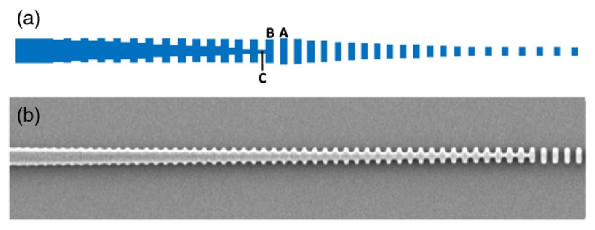
Trident structure: Instead of a single inverse taper, multiple auxiliary tapers are placed around the main waveguide. Hatori et al. demonstrated a 150 µm trident coupler on a 220 nm SOI platform, achieving polarization-insensitive high efficiency of -0.92 dB (80.9%, TE) and -0.94 dB (TM) [7].
Subwavelength Grating (SWG) couplers: A metamaterial approach that artificially tunes the effective refractive index by patterning sub-wavelength features directly in the silicon waveguide [7][8]. Benedikovic, Cheben et al. developed a multi-level SWG coupler combining partial and full etch regions, experimentally achieving -0.69 dB (85.3%) with 60 nm 3-dB bandwidth when combined with a metal reflector [8]. Simulation-based L-shaped SWG designs report -0.25 dB (~95%) [9], though this requires experimental validation.
https://doi.org/10.1364/OE.23.022553
Vertical edge coupler (Elephant coupler): To overcome the constraint of die edge dicing, silicon waveguide cantilevers are bent 90° upward using ion implantation (80 keV) or thermal annealing stress, enabling vertical end-fire coupling. A -2.2 dB (TE) coupling efficiency has been confirmed with lensed fiber at a 3 µm bend radius [2][7].
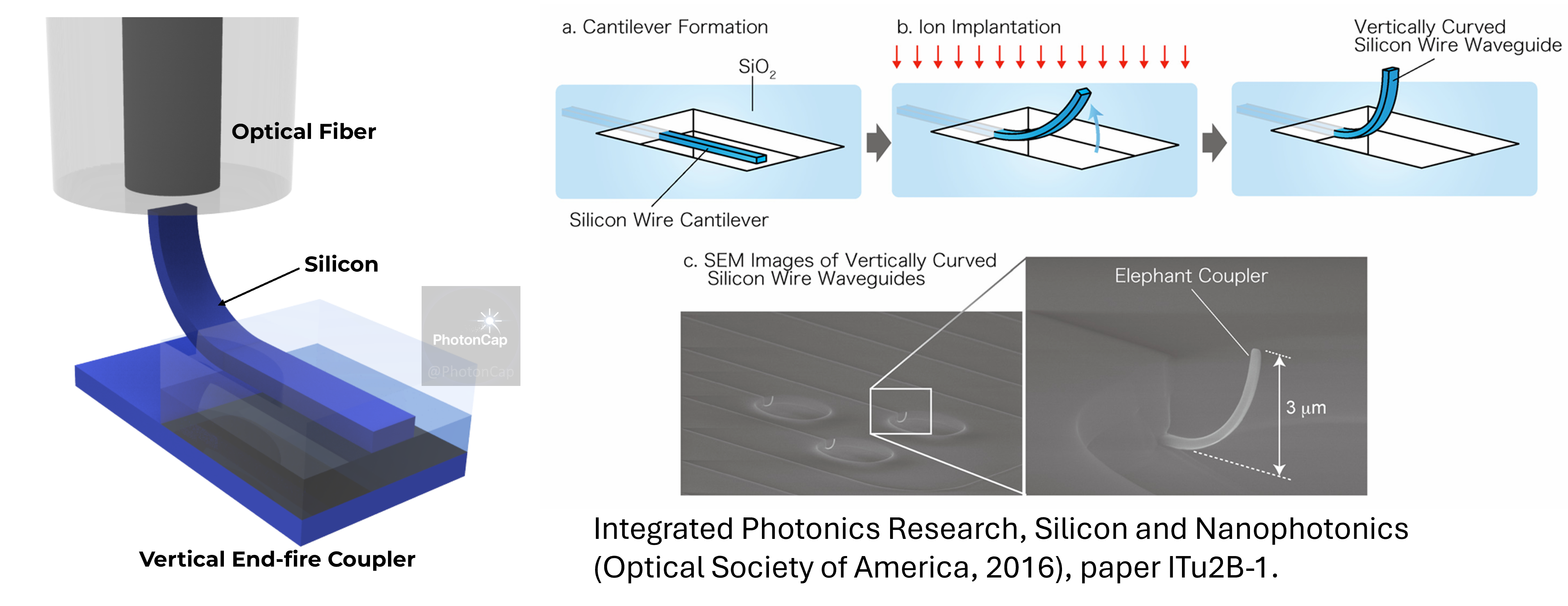
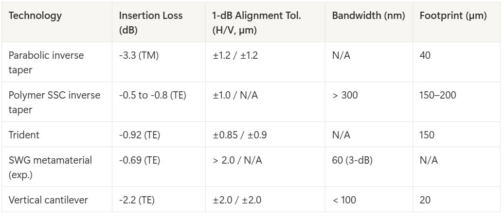
Table 1. Performance comparison of major edge coupling methods (Data: [2][5][7][8])
3.3. Packaging Limitations of Edge Coupling
Despite high efficiency and broadband performance, edge coupling has three key weaknesses in high-density system-level packaging. First, I/O ports can only be placed at the chip edge, creating a “Shoreline Bottleneck” that limits channel scaling. Second, dicing and polishing post-processes are mandatory to expose the coupler facet, fundamentally blocking wafer-scale inline testing. Third, the alignment tolerance is typically ±1–2 µm, requiring active alignment and directly reducing production throughput [2][5][7].
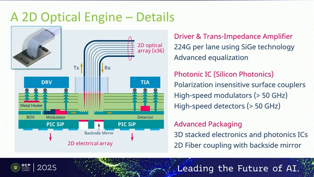
Industry efforts to circumvent these limitations are noteworthy. Peter Winzer, CTO of Nubis Communications, presented at OCP Global Summit 2025 an optical engine architecture combining 2D optical fiber arrays with surface grating coupling to implement large-scale optical I/O from the chip top surface instead of edge coupling [14]. This approach fundamentally resolves the shoreline bottleneck, coupling 36+ channels via a 2D fiber array in a single engine to meet CPO’s high-throughput demands. However, as discussed in Section 4, grating coupler bandwidth limitations and polarization dependence remain challenges.
4. Grating Couplers: Bending Light at the Surface
Grating Couplers (GC) are the most practical alternative circumventing the spatial and process constraints of edge coupling. By etching sub-wavelength periodic patterns in the device layer, light is diffracted out-of-plane, allowing placement anywhere on the chip with high layout flexibility and enabling wafer-scale parallel optical testing without dicing [5][7].
💡 [Analogy: A sunroof installed on the chip surface]
Rather than sending light out the chip’s edge (like an exit door), a grating coupler acts like a sunroof—sending light upward through the chip surface via periodic corrugations. Adding a bottom reflector beneath the waveguide dramatically improves coupling efficiency by redirecting downward-leaked light back up.
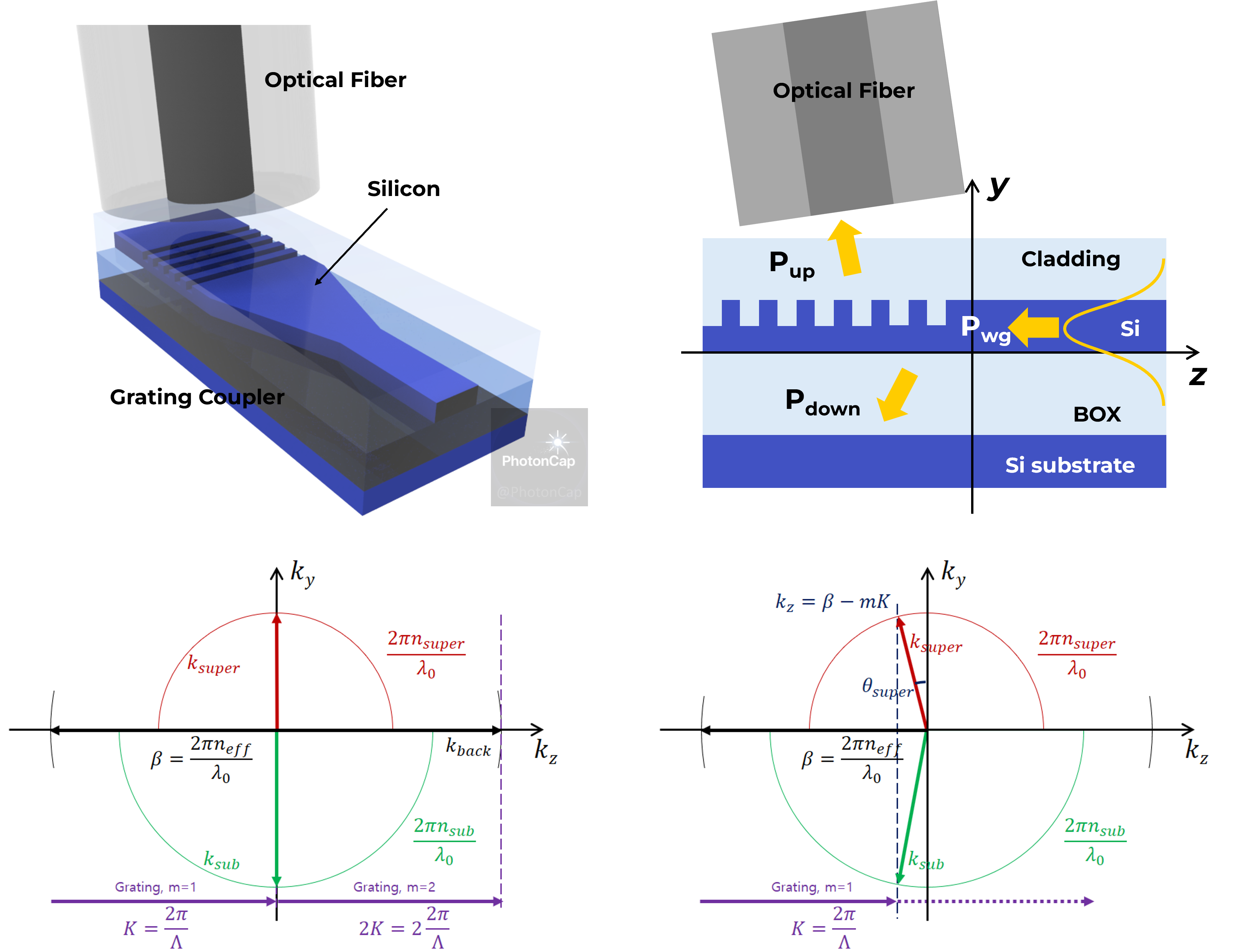
4.1. Operating Principle and Directionality Improvement
GC operation is governed by the Bragg condition. The relationship between the propagation constant β = 2πn_eff/λ₀ and the surface-parallel component of the diffracted wave k_m,z is k_m,z = β − mK (where K = 2π/Λ, m is the diffraction order) [5].
Designing for perfectly vertical emission (θ = 0°) causes the second-order diffracted wave to become a back-reflection toward the input waveguide, inducing parasitic Fabry-Perot oscillation. Therefore, off-normal emission angles of 8°–15° are typically used to collect only the first-order diffracted light and minimize back-reflection [5][7].
Shallow-etched (e.g., 70 nm depth) uniform grating couplers lose approximately 35–45% of incident optical power toward the substrate, making directionality a critical issue [7]. Key approaches to address this include:
Bottom Reflector introduction: Inserting Au, Al thin film, or Si/SiO₂ distributed Bragg reflector (DBR) below the BOX layer to redirect downward-diffracted light upward. When BOX thickness matches constructive interference conditions, directionality exceeds 90%, and combined with an apodized grating, -0.62 dB (~87%) coupling efficiency has been reported [7].
Poly-Si Overlay: A CMOS-compatible process that grows polycrystalline silicon on the grating to break vertical refractive index symmetry. A 150 nm overlay on 220 nm etch achieves 85% directionality at -1.08 dB. A single-crystal silicon nanomembrane (Si-nmb) overlay variant reports -1.6 dB loss with 44 nm 1-dB bandwidth [7].
Dual-level Etch and Slanted Gratings: Alternating shallow (70 nm) and full (220 nm) etches in one period, or using focused ion beam (FIB) to create 50–60° angled etches for a blazed effect. The dual-etch structure reports -1.3 dB loss with 52 nm 3-dB bandwidth [7].
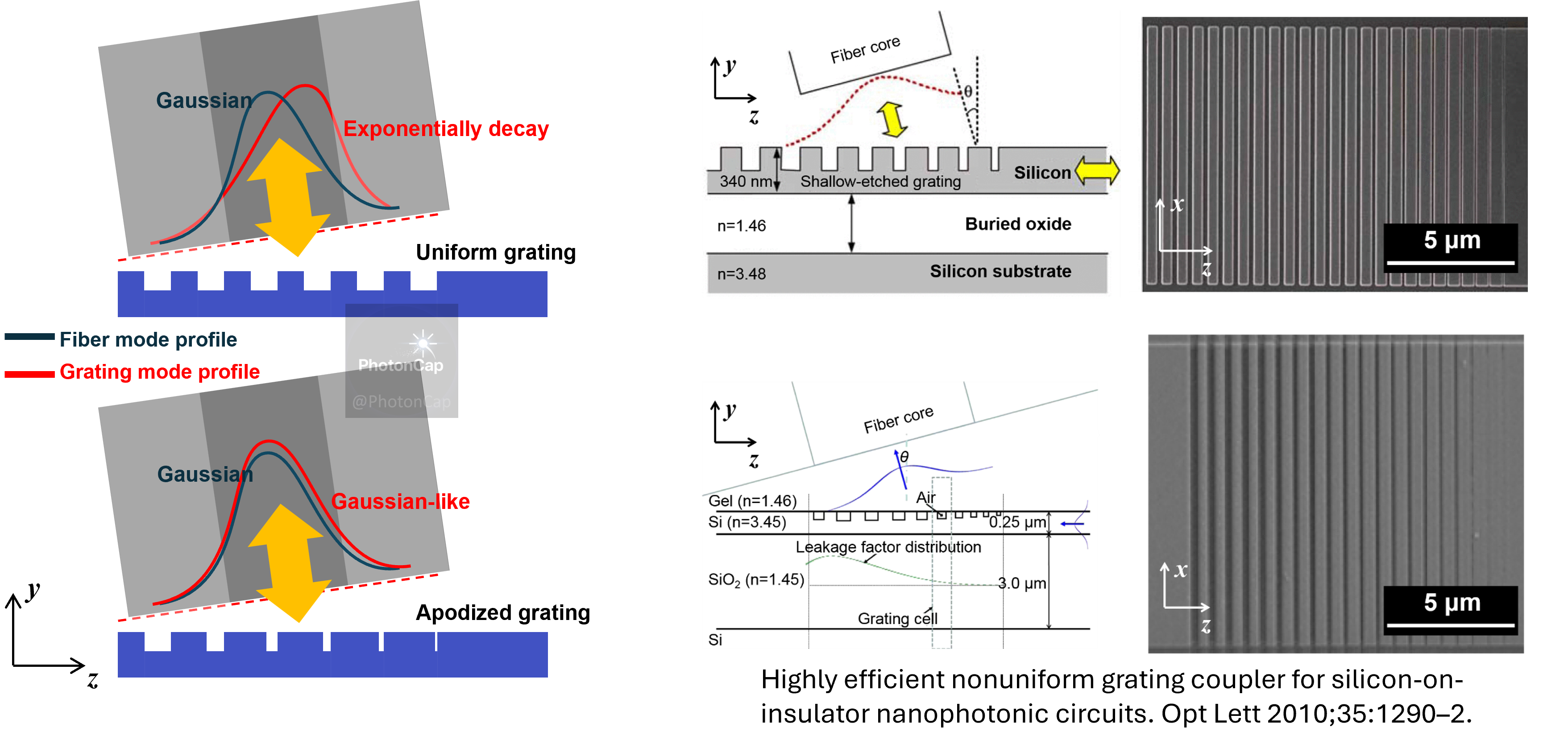
4.2. Apodization for Mode Matching
Even with improved directionality, mismatch between the fiber’s Gaussian beam profile and the grating emission profile causes mode matching loss. A uniform coupling strength (α) grating emits light in an exponential decay pattern (P(z) = P₀e⁻²αz), limiting overlap integral with the Gaussian mode to ~75% [7].
Linear chirp (FF = FF₀ − R·z) that gradually varies fill factor along propagation direction z corrects this. An apodized GC on a 260 nm SOI platform experimentally demonstrated -0.9 dB coupling efficiency [7].
4.3. 2D Polarization Diversity Grating Couplers
1D GCs exhibit extreme polarization dependence due to large effective index differences between TE and TM. To accommodate arbitrarily varying polarization states in telecom networks, 2D grating couplers that physically superimpose orthogonal 1D GCs are required. An optimized 2D-GC with aluminum reflector records -0.95 dB insertion loss and ~0.3 dB PDL at 1550 nm, serving as a key component in production-grade receiver modules [7].
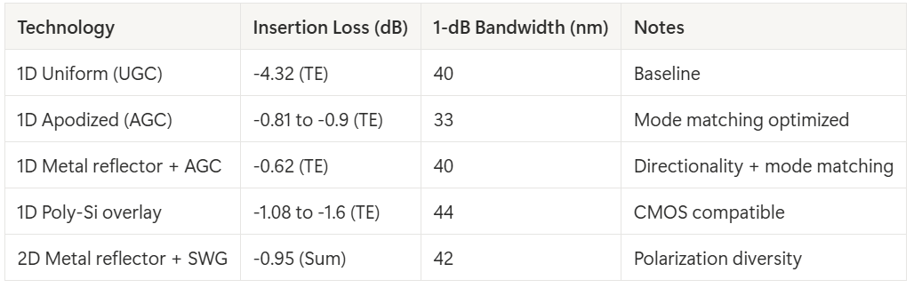
Table 2. Performance comparison of major grating coupling methods (Data: [5][7])
GC assembly tolerance of ±2.0–3.0 µm is wider than edge couplers, suitable for high-speed pick-and-place equipment. However, the 1-dB bandwidth of 30–50 nm is narrower than edge coupling (>100 nm), requiring additional bandwidth expansion such as Si₃N₄ dual-level couplers for broadband WDM or multi-band (O-band and C-band) applications [5][7].
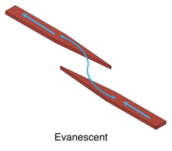
5. Adiabatic and Evanescent Coupling
5.1. Operating Principle
Adiabatic coupling is a technique where optical power gradually transitions between two waveguides via evanescent fields. While edge coupling completes coupling at the chip facet in one step, adiabatic coupling spreads mode transition across tens to hundreds of µm interaction regions. The beat length between two waveguides is defined as L_b = λ₀ / (n_eff,1 − n_eff,2), and the actual coupling region must be several to 10× this beat length to satisfy the adiabatic condition [2].
💡 [Analogy: Transferring cargo between two trains running side by side]
Instead of cutting and splicing rails, two trains (waveguides on different chips) run side by side in close proximity. As one gradually narrows and the other widens, the cargo (optical energy) naturally transfers from the narrowing to the widening train. This is the principle enabling inter-layer optical transfer without facet cutting.
This characteristic is useful not only for fiber-to-PIC coupling, but is particularly powerful in heterogeneous chip-to-chip 3D hybrid stacking. For example, when waveguides from a III-V compound semiconductor laser chip (top) and a silicon photonic chip (bottom) face each other across a tens-to-hundreds-nm DVS-BCB bonding layer, designing a “cross inverse taper” structure where both waveguide widths change inversely enables mode transition across the refractive index barrier [2].
5.2. HIC vs. LIC: Trade-offs by Refractive Index Contrast
Evanescent coupler packaging assembly tolerance is strongly influenced by waveguide refractive index contrast (Δn) [2].
High Index Contrast (HIC) systems (e.g., Si-Si): Δn of 0.5–2 requires adiabatic lengths exceeding 500 µm with multi-segment tapers for ±3 µm assembly tolerance. Coupling efficiency is sensitive to vertical gap errors and adhesive refractive index variations.
Low Index Contrast (LIC) systems (e.g., polymer/glass-Si): Ion-exchanged (IOX) waveguides or flexible polymer ribbons have very low Δn < 0.006. The adiabatic length increases to 1.5–2 mm for ±3 µm tolerance, but sensitivity to refractive index errors or thermal media changes is approximately 15× lower than HIC, providing significant packaging stability advantages [2].
Evanescent coupling theoretically achieves near-zero reflected power, insertion loss below 0.5 dB, and coupling bandwidth exceeding 100 nm. The most notable advantage is the ability to narrow pitch to 10 µm, securing density above 100 connections/mm. This exceeds the physical limit of conventional fiber arrays (8 connections/mm max) by more than 10×, attracting attention as a key technology for ultra-high-density CPO architectures [2].
6. Free-form and Mechanical Cantilever Couplers
6.1. Micro-lens/Mirror-based Free-form Coupling
Free-form couplers use two-photon polymerization (TPP), grayscale lithography, or nanoimprint lithography (NIL) to precision-print 45° total internal reflection (TIR) mirrors or collimating micro-curved lenses on the chip surface [2][10].
Light traveling horizontally in the waveguide hits the 45° mirror, deflects vertically (Z-axis), and expands its beam size (MFD) through the lens structure. By intentionally enlarging the beam diameter, the lateral assembly tolerance widens from ±2 µm to ±10–35 µm or more, and the Z-axis vertical separation also accommodates tens to hundreds of µm [2][10].
💡 [Analogy: Making the target 10× bigger]
Threading a hair through a needle eye (±1 µm tolerance) is slow and expensive. A free-form lens acts like a magnifying glass, expanding the beam diameter by 10× or more. Since the beam is wider, the target is larger, enabling stable coupling even with tens of µm chip misalignment—the key principle enabling optical assembly within the tolerance range of electrical bump equipment.
This optical relaxation accommodates solder bump (C4, Cu pillar) process tolerances in electronic packaging, making it the key mechanism for simultaneous electro-optical hybrid bonding (co-packaging). Free-form structures have low refractive index dispersion (±200 nm 1-dB bandwidth) and operate independently of TE/TM polarization [2][10]. Ranno et al. experimentally achieved 0.8 dB coupling loss and >180 nm 1-dB bandwidth between SMF-28 and a 220 nm SOI platform [10]. However, the serial nature of TPP fabrication requires transition to multi-beam exposure or NIL-based parallel replication for high-volume production.
6.2. Stress-Induced Mechanical Cantilever Coupling
An alternative approach physically bends the waveguide itself upward. Applying high-temperature (770°C) oxide stress to substrate-released silicon waveguides, or implanting silicon ions (Si⁺, 80 keV, dose 1.7 × 10¹⁶ cm⁻²) to create lattice defects, generates surface stress gradients that bend the cantilever waveguide 90° [2].
This method achieves edge coupling facets in the vertical direction with 3–5 µm bend radii, enabling fiber coupling at wafer scale without dicing. However, high ion implantation doses increase waveguide propagation loss (up to 40 dB/mm), and research on novel cladding materials and polymer SSC structures to mitigate this is ongoing [2].
7. Photonic Wirebonding (PWB): Nullifying Alignment Error
One of the most advanced packaging technologies is Photonic Wirebonding (PWB), inspired by electrical wirebonding [2][11]. If the packaging bottleneck lies in the process of aligning components to exact positions, PWB takes the reverse approach: place components approximately, then create the optical path afterward.
💡 [Analogy: Place the islands first, draw the bridge later]
Traditional packaging precisely aligns two islands (chips) to a pre-built bridge. PWB reverses this: place the two islands with generous tolerance, then use a 3D scanner to determine actual positions and a 3D printer (laser) to draw a custom bridge on the spot. Since the software compensates for any chip misalignment, the variable of positional alignment error itself is eliminated.
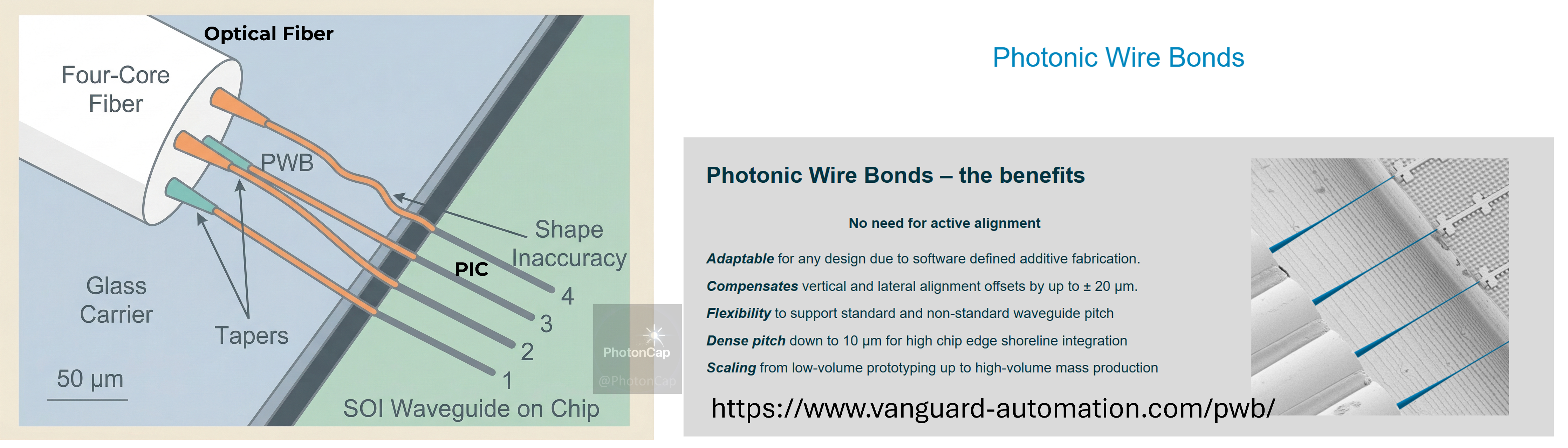
The process works as follows: two chips (e.g., laser chip and silicon photonic chip) are placed on the packaging substrate with ±50 µm mechanical tolerance. A high-resolution 3D machine vision system then scans each chip’s I/O waveguide facet coordinates at nanometer precision. The system calculates the optimal 3D spline waveguide trajectory connecting the two coordinates, and a femtosecond laser TPP 3D printer exposes a photocurable polymer resin along the trajectory to form a 3D polymer optical waveguide connecting the two chips [2][11].
The core value is the fundamental elimination of coupling loss due to alignment error. Recent research has demonstrated 0.7 dB insertion loss with ~0.8 Tbit/s data transmission [11], and 1.6 dB or less over a 1280–1580 nm ultra-broadband (>300 nm) range [2]. Variant techniques such as SCRIBE (mesoporous silicon scaffold-based) have also been developed to support flexible multi-mode and single-mode interconnection [12].
However, since the laser sequentially draws each path, throughput (tens of seconds per bond) is insufficient for high-volume production lines processing tens of thousands of I/Os. Research on multi-beam lenses and projection-based light-sheet exposure for electrical wire bonder-level speeds (<0.1 s/bond) is actively progressing [2].
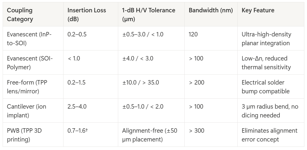
Table 3. Performance comparison of evanescent, free-form, cantilever, and PWB coupling (Data: [2][10][11][12])
†PWB insertion loss note: 0.7 dB is per bond (Billah 2018 [11]); 1.6 dB is total for both interfaces in C-band (Lindenmann 2012 [11]). Broadband (1240–1580 nm) total for both interfaces is 2.5 ± 1.1 dB.
8. Summary, Conclusions, and Part 2 Preview
As explored in this article, the optical I/O challenge in silicon photonics fundamentally originates from the mode mismatch between 10.4 µm MFD optical fiber and ~0.1 µm² cross-section submicron waveguides. To bridge this 1,000× gap, diverse approaches have evolved: edge coupling (inverse taper, SWG), grating couplers (apodization, reflectors), evanescent coupling, free-form lenses, cantilevers, and photonic wirebonding.
Each technology presents different trade-offs across five axes—insertion loss, alignment tolerance, bandwidth, polarization dependence, and manufacturing scalability—and no single technology satisfies all requirements. Industry trends show a clear shift from active alignment at the chip periphery toward passive alignment-compatible structures that route through the chip surface or substrate interior. Grating couplers (§4) enable wafer-scale passive alignment anywhere on the chip surface; free-form couplers (§6) achieve wide ±10–35 µm tolerance through beam expansion; and photonic wirebonding (§7) renders alignment irrelevant through post-fabrication correction. Nubis (§3.3 [14]) circumventing the shoreline bottleneck with 2D optical arrays and surface grating coupling, and Marvell TX9190 (§1 [15]) placing dozens of optical engines around the ASIC, are both designs predicated on high-throughput mass assembly.
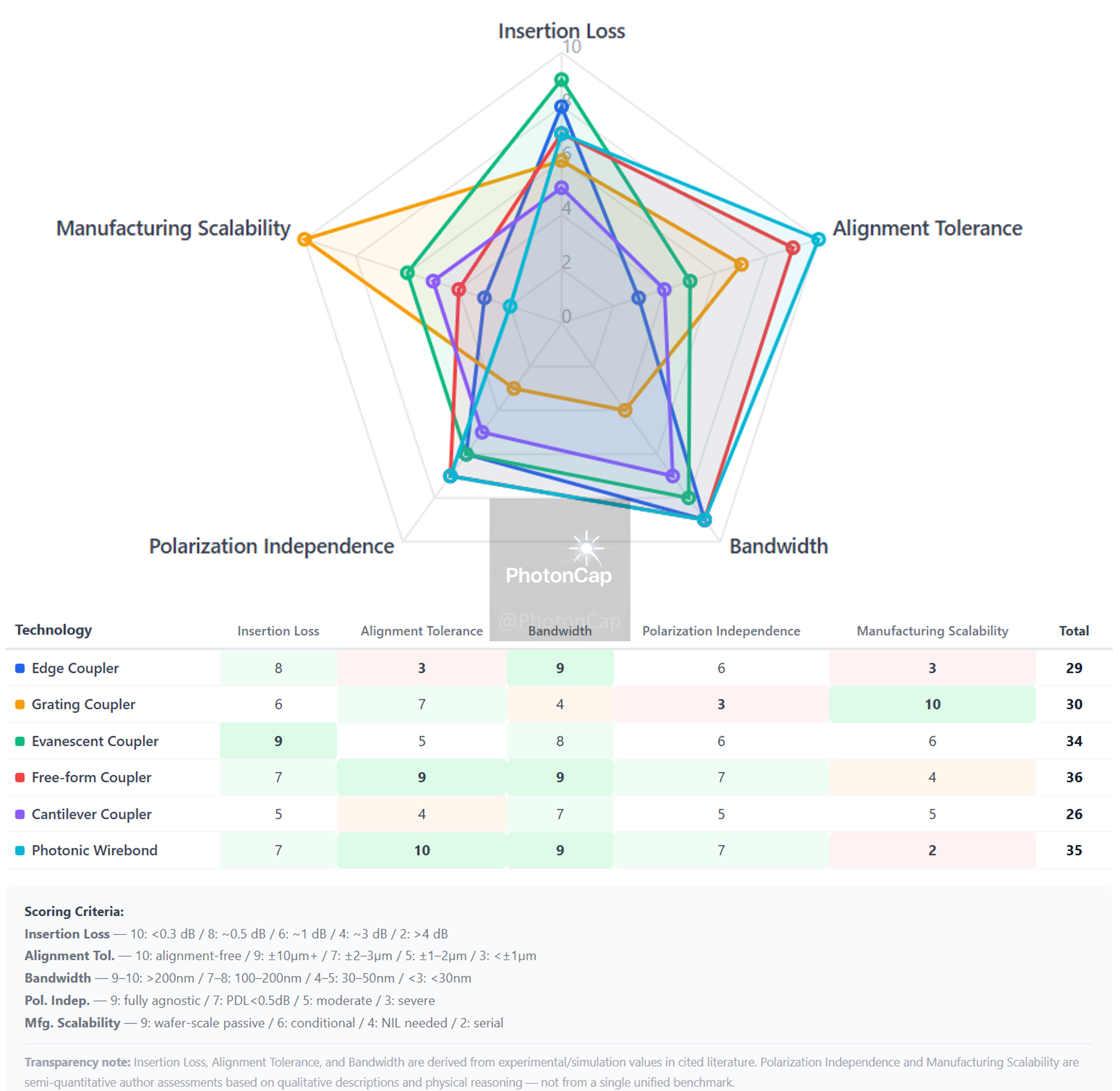
Conclusion: Channel Count Scaling Is the Next Battleground
In the author’s view, increasing channel count per package will be the most dominant technical direction as CPO evolves. As already evident in the Marvell TX9190, a single switch requires hundreds of F2C junctions, and this number will grow to thousands in next-generation 3D CPO. Insertion loss remains a critical metric, but ultimately what the system demands is simultaneously achieving low loss and high channel density.
Edge coupling can achieve the lowest loss below 0.5 dB, but faces fundamental limits in channel scaling due to the shoreline bottleneck. However, V-groove-based passively aligned fiber arrays can implement edge coupling without active alignment [16], representing meaningful progress in production throughput. Evanescent coupling can also achieve sub-0.5 dB loss, but the hundreds-of-µm-long coupling regions pose compatibility challenges with large-area packaging. While these technologies are clearly advancing in insertion loss, passive alignment compatibility, and other dimensions, the structural limitation of 1D shoreline constrains dramatic throughput scaling.
In contrast, grating couplers and free-form couplers can utilize the entire chip surface for 2D array placement, offering high degrees of freedom for channel scaling. Bringing these approaches’ loss down to sub-dB levels while securing manufacturing compatibility is one promising direction. Another compelling direction is the use of glass substrates (Glass Interposer/Substrate). Glass has a refractive index (~1.5) nearly identical to fiber cladding, fundamentally favoring fiber-to-PIC mode matching and enabling dramatic insertion loss reduction. Furthermore, glass substrates can be scaled to much larger areas than silicon dies, substantially alleviating the shoreline bottleneck. Ultimately, whoever first implements at production scale a method to increase channel count while reducing loss—whether through surface coupling loss improvement or glass substrate mode matching optimization—will determine the outcome of the CPO era.
Part 2 (subscriber-only) broadens the scope. We compare which F2C approaches Nvidia, Broadcom, Marvell, Nubis, and other major companies have actually chosen; dig into why glass substrates are beginning to be called “the second silicon” as previewed in Part 1; explore Photonic Vias where light penetrates substrates vertically; the assembly nightmare where curing epoxy destroys alignment; and beyond CPO switches—optically connected memory, neuromorphic chips that compute with light, quantum photonics handling single photons, thumbnail-sized LiDAR, and biosensors diagnosing from a single blood drop—the next-generation battlegrounds that silicon photonics packaging is opening up.
As of 3/8, the Part 2 draft is complete but topics are still being refined. If you have topics you’d like covered or questions, anyone is welcome to drop a comment — subscriber suggestions will be prioritized.
References
[1] NVIDIA, “NVIDIA Announces Spectrum-X Photonics, Co-Packaged Optics Networking Switches to Scale AI Factories to Millions of GPUs,” GTC 2025 Press Release (March 18, 2025).
https://nvidianews.nvidia.com
— SemiAnalysis, “Co-Packaged Optics (CPO) – Scaling with Light for the Next Wave of Interconnect” (2026).

[2] Weninger, D., Serna, S., Ranno, L., Kimerling, L., & Agarwal, A., “Advances in waveguide to waveguide couplers for 3D integrated photonic packaging,” Light: Science & Applications 15, 17 (2026). https://doi.org/10.1038/s41377-025-02048-w
[3] Ranno, L. et al., “Integrated Photonics Packaging: Challenges and Opportunities,” ACS Photonics 9(11), 3467–3485 (2022). https://doi.org/10.1021/acsphotonics.2c00891
[4] Optics & Photonics News, “AI Factories: Photonics at Scale” (November 2025); Semiconductor Engineering, “Silicon Photonics Manufacturing Ramps Up” (May 2024); CITC/vario-optics, “Advancing the semiconductorisation of photonic chip packaging,” PIC Magazine.
[5] Son, G. et al., “High-efficiency broadband light coupling between optical fibers and photonic integrated circuits,” Nanophotonics 7(12), 1845–1864 (2018). https://doi.org/10.1515/nanoph-2018-0075
[6] Corning, SMF-28 Ultra Optical Fiber Product Specification. MFD: 10.4 ± 0.5 µm at 1550 nm, Core diameter: 8.2 µm. https://www.corning.com/optical-communications
[7] Marchetti, R. et al., “Coupling strategies for silicon photonics integrated chips,” Photonics Research 7(2), 201–239 (2019). https://doi.org/10.1364/PRJ.7.000201
[8] Benedikovic, D., Cheben, P. et al., “Subwavelength index engineered surface grating coupler with sub-decibel efficiency for 220-nm silicon-on-insulator waveguides,” Optics Express 23(17), 22628–22635 (2015). https://doi.org/10.1364/OE.23.022628 — Experimental: -0.69 dB (85.3%) with metal reflector.
[9] Benedikovic, D. et al., “Sub-decibel silicon grating couplers based on L-shaped waveguides and engineered subwavelength metamaterials,” Optics Express 27(18), 26239–26250 (2019). https://doi.org/10.1364/OE.27.026239 — Simulation: -0.25 dB (~95%).
[10] Ranno, L., Sia, J. X. B. et al., “Highly efficient fiber to Si waveguide free-form coupler for foundry-scale silicon photonics,” Photonics Research 12(5), 1055–1066 (2024). https://doi.org/10.1364/PRJ.514999
[11] Billah, M. R. et al., “Hybrid integration of silicon photonics circuits and InP lasers by photonic wire bonding,” Optica 5(8), 876–883 (2018). https://doi.org/10.1364/OPTICA.5.000876 — 0.7 dB insertion loss, ~0.8 Tbit/s demonstration. Juodkazis, S., Light: Science & Applications 9, 72 (2020). Lindenmann, N. et al., Optics Express 20, 17667–17677 (2012) — First PWB concept demonstration.
[12] Richards, C. A. et al., “Low loss fiber-coupled volumetric interconnects fabricated via direct laser writing,” Optica 11(7), 995 (2024). https://doi.org/10.1364/OPTICA.524899 — SCRIBE technique, 2.14 dB insertion loss (fiber-PIC-fiber).
[13] Minkenberg, C. et al., “Co-packaged datacenter optics: Opportunities and challenges,” IET Optoelectronics 15(2), 77–91 (2021). https://doi.org/10.1049/ote2.12020 — Figure 6: CPO roadmap. Low journal IF but 150+ citations as a widely referenced CPO evolution framework.
[14] Winzer, P. (CTO, Nubis Communications), “Resolving Operational Barriers to AI Scale Up with Co-Packaged Copper Optics Sockets,” OCP Global Summit 2025.
— 2D optical array + surface grating coupling optical engine architecture.
[15] Marvell Technology / ServeTheHome, “Marvell TX9190 Liquid-Cooled CPO Switch at OCP 2025” (November 2025). https://www.servethehome.com/marvell-tx9190-liquid-cooled-cpo-switch-at-ocp-2025/ — 51.2 Tbps liquid-cooled CPO switch reference design, co-developed with Jabil. Figure 1-c source.
[16] Nagarajan, R. et al., “2.5D Heterogeneous Integration for Silicon Photonics Engines in Optical Transceivers,” IEEE Journal of Selected Topics in Quantum Electronics 29(3), 8200209 (2023). https://doi.org/10.1109/JSTQE.2022.3214418 — Passively aligned fiber array assembly for 2.5D SiPh engine. Figure 1-c bottom inset source.
I understood at least *some* of that, thanks for helping me replasticise my neurons
Very useful information, thank a lot.