AXT Inc. (AXTI) Deep Dive: The Hidden Bottleneck in AI Optical Interconnects

1. The Hook: Why Pay Attention to Indium Phosphide (InP) and AXT Inc. Now?
From the second half of 2025 through the first quarter of 2026, one of the most volatile and exceptionally rewarding stocks in the global market has been AXT Inc. (NASDAQ: AXTI), a Silicon Valley-based manufacturer of compound semiconductor substrates. Languishing at around $1 per share in early 2025 (with a 52-week low of $1.13), the stock surged past $37.58 by March 1, 2026, delivering a staggering trailing 12-month return of 2,268% (and over 3,174% from its 52-week low). In the blink of an eye, its market capitalization ballooned from micro-cap obscurity to approximately $2 billion.
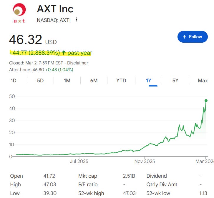
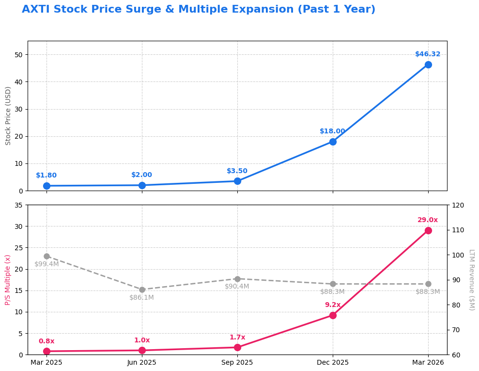
Beneath this historic stock price explosion lies a highly paradoxical set of financial metrics. AXT Inc.’s total revenue for fiscal year 2025 was $88.3 million, down 11.1% year-over-year, and its GAAP net loss widened to $21.3 million. Furthermore, Q4 2025 revenue came in at just $23.0 million, missing market expectations due to geopolitical export controls from China. With core fundamentals like revenue growth and profitability clearly impaired, why is the market enthusiastically assigning this company an extreme trailing Price-to-Sales (P/S) multiple of roughly 22.9x (adjusted for the December 2025 new share issuance)?
The answer lies in the most critical bottleneck of AI cluster expansion—Optical Interconnects—and the status of Indium Phosphide (InP) as a virtually irreplaceable material physically capable of resolving this bottleneck.
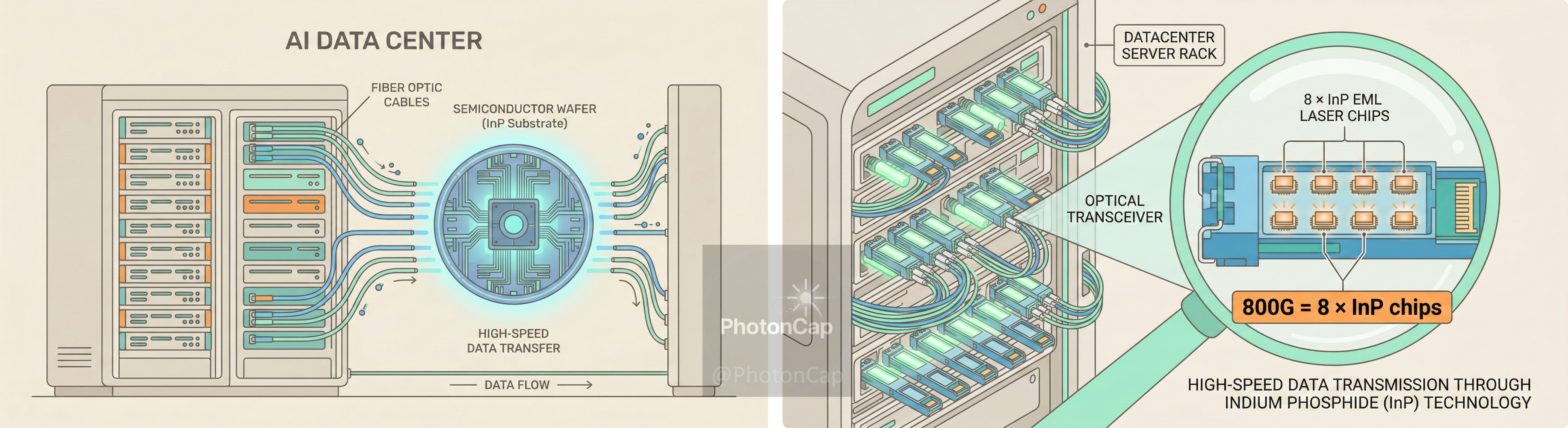
Next-generation AI data centers powered by NVIDIA’s H200/B200 infrastructure and Broadcom’s Tomahawk 5 switches are pushing node-to-node data transmission speeds beyond 800G to 1.6T (Terabits per second). For tens of thousands of GPUs to operate as a single massive computer, latency and power consumption must be aggressively minimized. Traditional copper wiring has hit its physical limits regarding signal integrity and heat dissipation. In the optical fiber networks replacing copper, InP is the mandatory substrate for the core components that generate (Lasers) and detect (Photodetectors) light.
2. Company Background & Vertically Integrated Business Model
Founded in 1986 and headquartered in Fremont, California, AXT Inc. is a materials science company that develops and manufactures high-performance compound and single-element semiconductor wafer substrates. While traditional silicon (Si) wafers dominate the broader semiconductor industry, they fall short of the extreme high-frequency, high-power, and specific optoelectronic requirements of advanced applications. To fill this gap, AXT supplies critical substrates made of Indium Phosphide (InP), Gallium Arsenide (GaAs), and Germanium (Ge).
The most formidable strategic moat in AXT’s business model is its heavily vertically integrated supply chain. While players like JX Nippon internalize some raw materials, AXT is widely recognized as having one of the deepest and most comprehensive vertical integration models among publicly traded substrate suppliers—spanning from raw mineral sourcing and refining to final wafer production. All manufacturing operations are conducted through its Beijing-based subsidiary, Beijing Tongmei Xtal Technology Co., Ltd. (Tongmei).
Through Tongmei, AXT holds strategic stakes in over ten raw material joint ventures (JVs) in China, internalizing the production of mission-critical materials. Crucially, these JVs extract and refine raw minerals into the extreme purity levels required for semiconductor manufacturing. They process standard 4N (99.99%) gallium into ultra-high purity 5N, 6N (99.9999%), 7N, and even 8N (99.999999%) gallium, while also producing high-purity indium, germanium dioxide, arsenic, and pyrolytic boron nitride (pBN) crucibles.
This model provides AXT with industry-leading cost advantages and shorter lead times compared to competitors relying on external suppliers. However, it operates as a double-edged sword. Because both manufacturing and raw material sourcing are overwhelmingly concentrated in China, AXT is highly exposed to severe geopolitical vulnerabilities amid escalating US-China trade tensions.
3. Technical Deep Dive: Why InP over GaAs or Silicon?
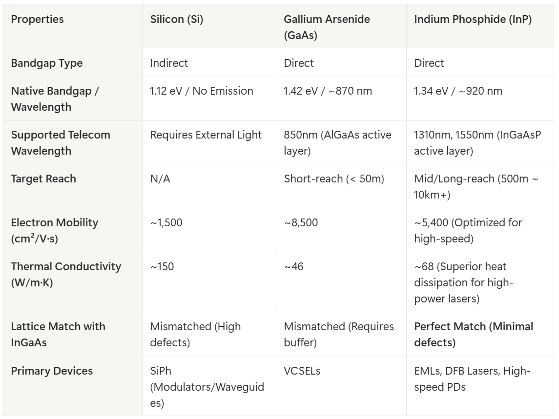
When discussing semiconductor substrates, 12-inch (300mm) silicon wafers are the first to come to mind, powering over 95% of the global market. However, when entering the realm of “Optoelectronics”—converting electrical signals to photons and vice versa—silicon reveals a fatal physical flaw. This is due to the structural difference in energy bandgaps. Silicon is an Indirect Bandgap material. When an electron drops from the conduction band to the valence band to release energy, a change in momentum is required. Consequently, the energy is mostly dissipated as heat (phonons) rather than light (photons). Simply put, it is physically impossible to build an efficient, native light-emitting laser out of silicon.
💡 [Concept Analogy] Indirect vs. Direct Bandgap A Direct Bandgap material is like someone jumping straight off a cliff into the water, immediately creating a massive splash (light). An Indirect Bandgap material (like Silicon) is like someone jumping, but hitting a protruding rock on the way down; the impact is absorbed by the rock (heat), and they barely make a splash when they hit the water (no light).
3.1. The Physics of Bandwidth and Wavelength: 850nm vs. 1310/1550nm
In optical communication systems, the absolute metric dictating transmission distance and quality is the wavelength of light. When light travels through silica-based optical fibers, signal attenuation (due to Rayleigh scattering and infrared absorption) varies drastically by wavelength. The optimal “magic bands” for minimum signal loss are the O-band (1310nm) and the C-band (1550nm). It is crucial to distinguish between a substrate’s native emission wavelength and the telecom wavelengths it can support via epitaxy. The bandgap energy of a semiconductor is inversely proportional to the wavelength of light it emits (λ=1240/Eg).
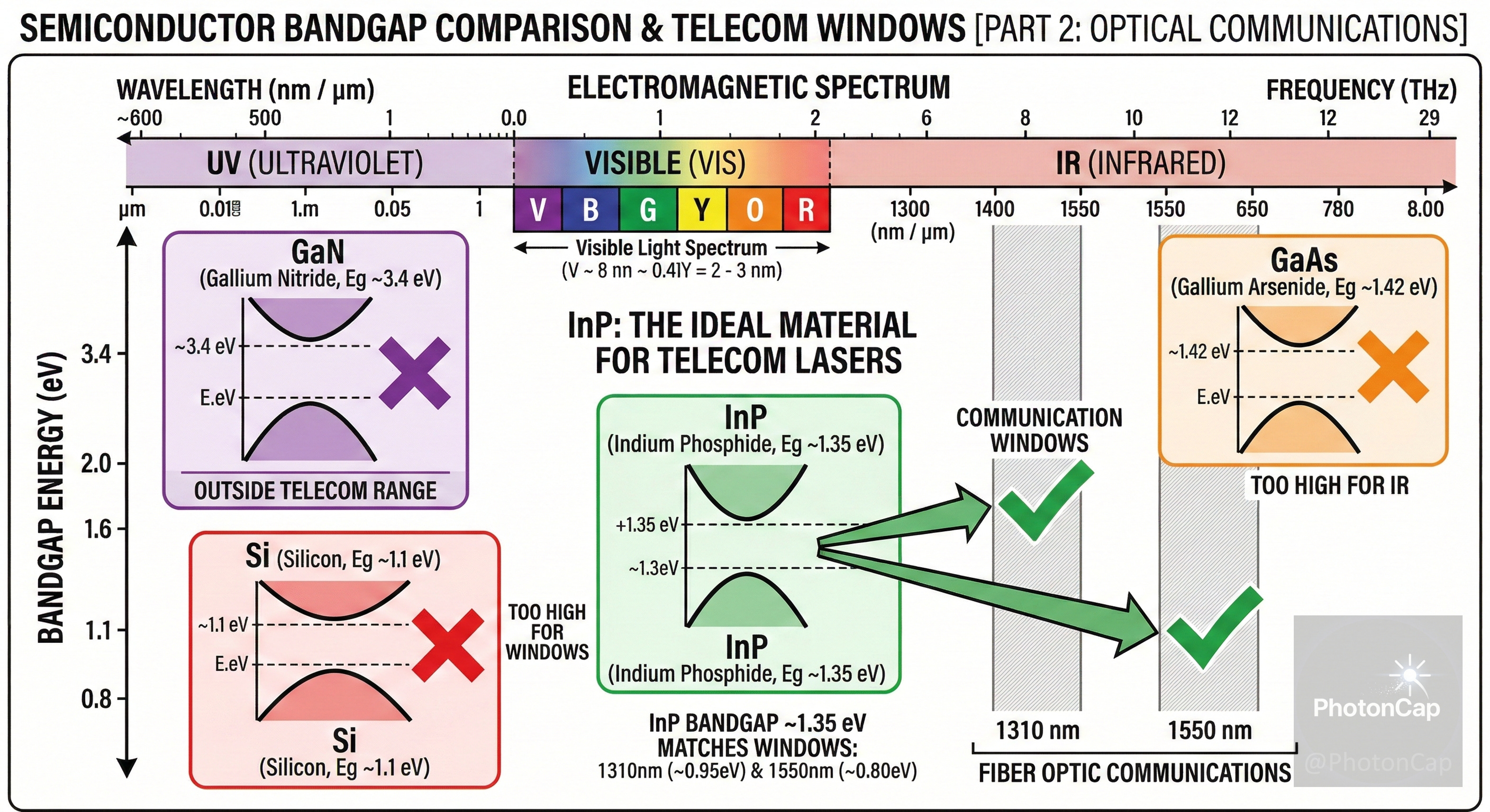
• The Limits of Gallium Arsenide (GaAs): A GaAs substrate has a native bandgap of ~1.42 eV (translating to ~870nm). By growing thin layers like AlGaAs on top, it primarily produces lasers emitting at 850nm. However, the 850nm wavelength suffers from severe signal attenuation and chromatic dispersion in optical fibers. Therefore, GaAs VCSELs are strictly limited to short-reach communications (under 50 meters), such as intra-rack connections.
• The Dominance of Indium Phosphide (InP): A pure InP substrate has a bandgap of ~1.34 eV (~920nm). However, InP dominates optical communications not because the substrate itself emits 1550nm light, but because it is the only “base substrate” that can perfectly support the defect-free, lattice-matched growth of active layers (like InGaAsP or InAlGaAs) that precisely generate the golden 1310nm and 1550nm wavelengths. These wavelengths experience near-zero signal loss, perfectly supporting mid-reach (500m) to long-haul (2km to 10km+) data center interconnects.
As AI models scale to trillions of parameters, data centers are forced to scale out, increasing the physical distance between GPUs. To transmit massive 1.6T bandwidths over hundreds of meters without loss, the industry is forced to transition away from 850nm GaAs VCSELs toward high-performance EML and DFB lasers built on InP platforms.
3.2. The Core of the Receiver: Photodetectors (PD) and Lattice Matching
The true value of InP extends beyond the transmitter (Tx) to the receiver (Rx) end, specifically in Photodetectors (PD) that convert light back into electrical signals.
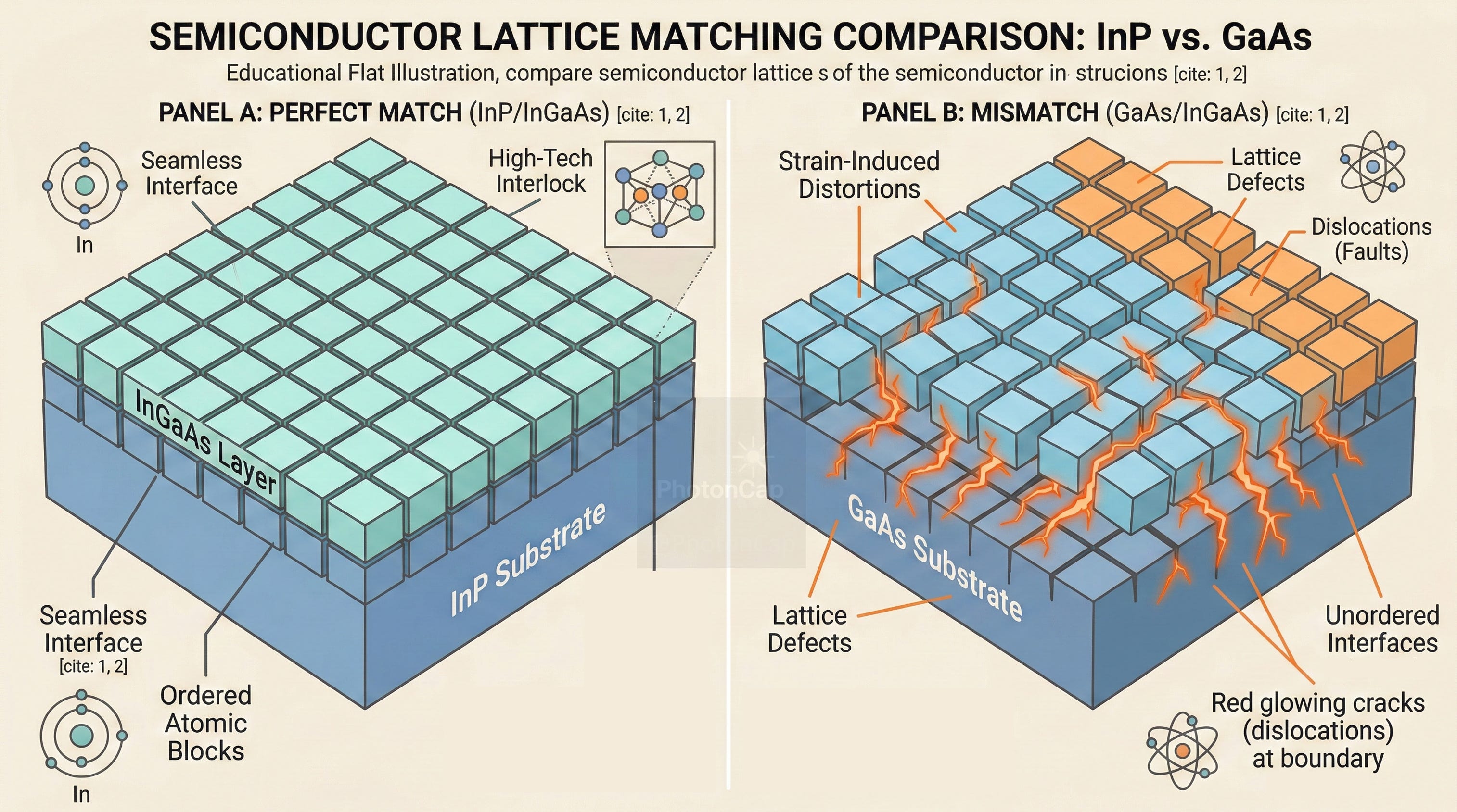
A receiver’s performance is dictated by bandwidth (response speed) and dark current (noise). The material that absorbs 1310nm and 1550nm light fastest and most efficiently is the Indium Gallium Arsenide (InGaAs) alloy. The key is the substrate upon which this InGaAs active layer is grown via epitaxy.
When stacking materials atom by atom, if the Lattice Constant (atomic spacing) between the substrate and the top layer differs, the layer warps and cracks, generating massive defects (dislocations). Remarkably, an InP substrate (lattice constant 5.869Å) provides a perfect lattice match for the specific InGaAs composition (In0.53Ga0.47As) required to absorb the 1550nm band.
Conversely, forcing InGaAs growth onto a cheaper GaAs or Si substrate results in a severe lattice mismatch, creating a high Threading Dislocation Density. These micro-defects cause leakage currents, sharply increasing the device’s Dark Current. In ultra-high-speed 1.6T communications, where detecting incredibly faint signals is paramount, a raised noise floor from dark current causes fatal data loss.
Optical Telecom Substrate Material Comparison