
The Polymer That Tower Chose — LWLG × TSEM Opens a New Chapter in Silicon Photonics

Intro
One headline dropped right after the close today (March 11, 4:30 PM ET).
Lightwave Logic (NASDAQ: LWLG) and Tower Semiconductor (NASDAQ: TSEM) signed a development agreement. The deal: integrate LWLG’s electro-optic (EO) polymer modulator reference designs into Tower’s PH18 silicon photonics PDK (Process Design Kit) [1].
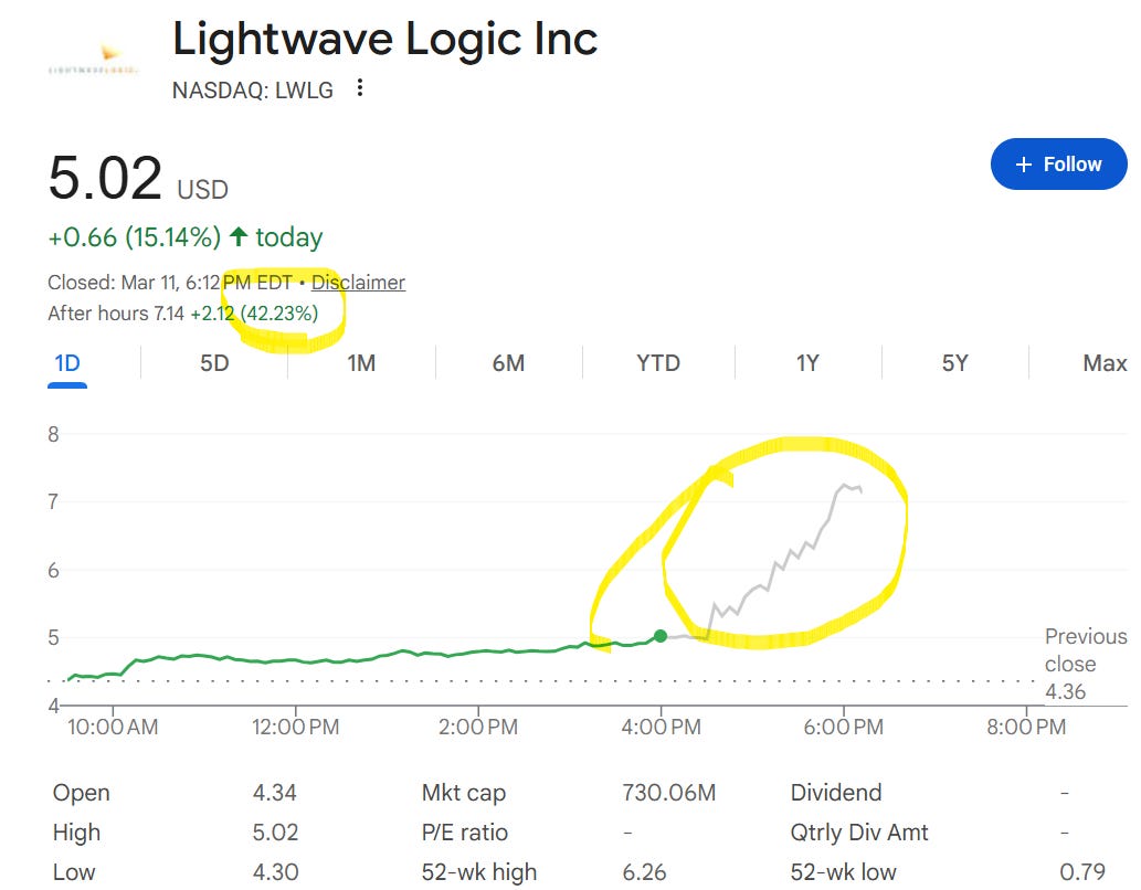
The market had already spoken before the formal announcement. LWLG rose +15.14% (+$0.66) during the regular session, and the official press release came right after the close (4:30 PM ET) [1]. In extended-hours trading, the stock hit a high of $7.28 (roughly +67% from the previous close of ~$4.36). The stock moving before the announcement suggests the market was already sensing and front-running the deal.
Here’s why this matters:
Tower Semiconductor — the foundry rapidly expanding its silicon photonics presence — just made its first formal bet on EO polymers as the “next-gen modulator material.”
The timing is worth noting. Just nine days ago (March 2), NVIDIA announced $2 billion investments each in Lumentum and Coherent — $4 billion total — for advanced optics R&D and US manufacturing [21]. Jensen Huang personally framed it as building “the next generation of gigawatt-scale AI factories” through silicon photonics [21]. And now, today, the TSEM-LWLG agreement drops. This isn’t an isolated event — it’s part of an accelerating chain of signals that AI optical infrastructure is entering a new phase.
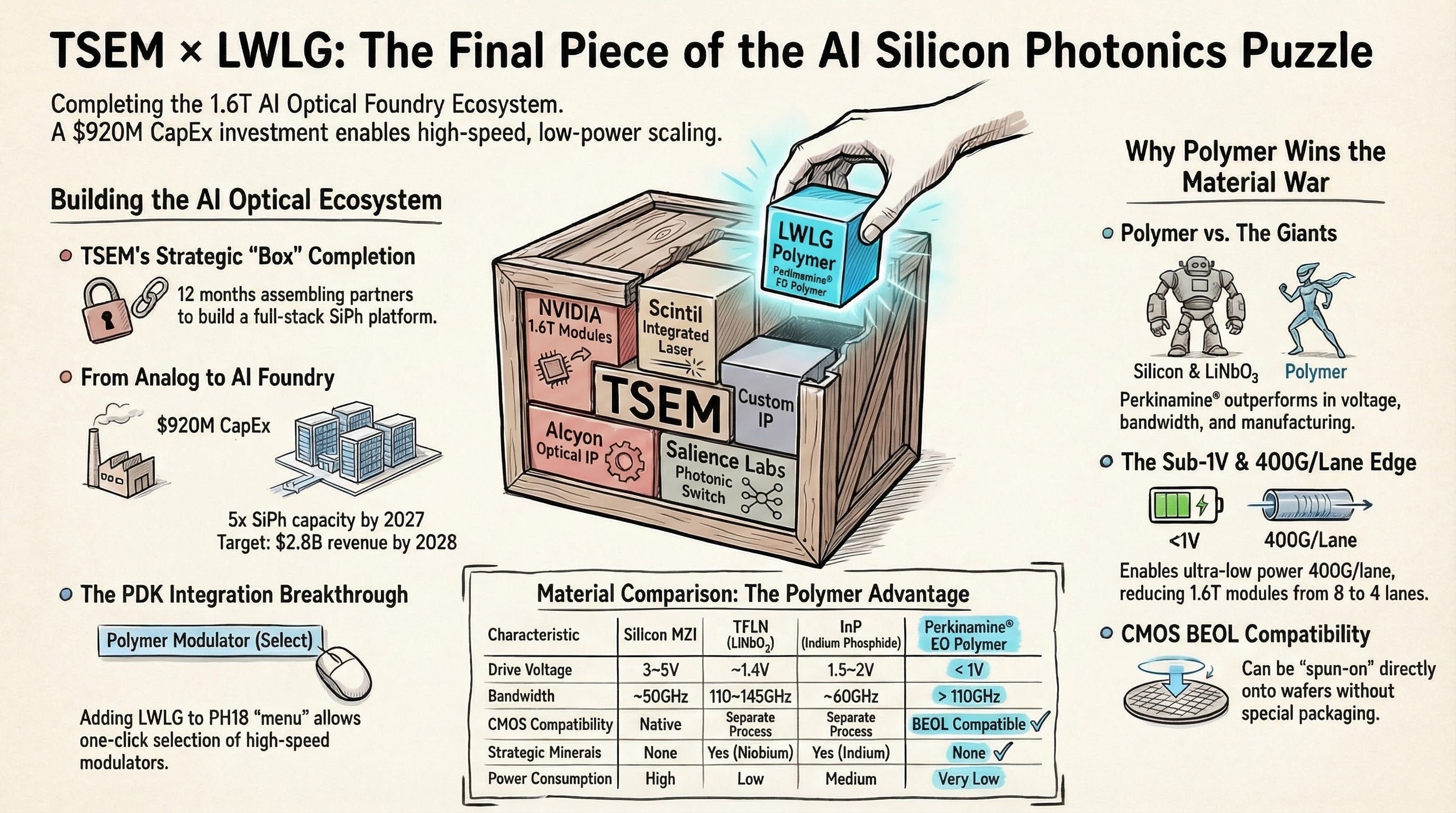
Over the past 12 months, TSEM has been steadily building out its silicon photonics (SiPho) ecosystem. NVIDIA collaboration for 1.6T optical modules. Scintil for DWDM lasers. Salience Labs for optical switches. Each of those partnerships addressed a key layer of AI datacenter optical infrastructure. And today, a “materials” layer was added to that stack.
Today we’ll use TSEM’s SiPho strategy as our anchor to walk through LWLG’s technical moat, what this agreement really means, and where we go from here.
Background: TSEM’s SiPho Buildout
Starting with the financials
Tower Semiconductor’s Q4 2025 earnings were impressive. Revenue of $440 million (all-time record), up 14% YoY and 11% QoQ [2]. Full-year 2025 revenue came in at $1.57 billion, up 9% from 2024, with net income of $220 million [2].
But here’s the number that really jumps out. TSEM’s silicon photonics revenue went from $106 million in 2024 to $228 million in 2025 — more than doubling in a single year [3]. That’s roughly 15% of total revenue, but in terms of growth rate, SiPho has been the primary growth driver for the company. CEO Ellwanger noted on the earnings call that of the $82 million company-wide revenue increase from Q1 to Q4, about $40 million flowed through to net income — an incremental net margin of roughly 49% at the corporate level [3]. This isn’t a SiPho-only figure; it reflects the overall mix improvement as higher-value photonics revenue became a larger share of the total.
¹ SiPho revenue figure as cited in TSEM’s earnings call. Appears to be reported separately from SiGe RF infrastructure revenue, though exact segment definitions should be confirmed against official IR materials.
CEO Russell Ellwanger called it “value-based growth.” Translation: they’re selling expensive chips, and lots of them.
What’s even more telling is the forward investment. TSEM announced a total of $920 million in CapEx for SiPho and SiGe expansion. The plan targets full installation and qualification of all equipment by Q4 2026, with full production starts commencing in 2027. At completion, SiPho wafer starts are projected to reach 5x+ the Q4 2025 monthly run-rate [4]. The long-term financial model targets $2.84 billion in revenue by 2028, with 39.4% gross margin and 31.7% operating margin [5].
Why do these numbers matter?
$920 million in CapEx is roughly 60% of TSEM’s annual revenue. This isn’t just a capacity expansion — it’s a declaration that the company is transforming its identity from “specialty analog foundry” to “AI optical infrastructure foundry.”
And backing up that declaration, TSEM has been systematically building its SiPho ecosystem over the past 12 months. Here’s the timeline:
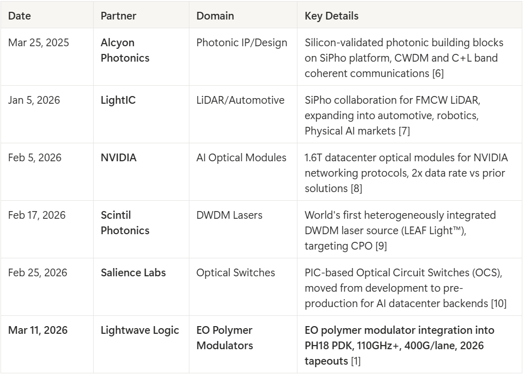
See the pattern?
Alcyon provides design tools (IP blocks), LightIC expands into new markets (LiDAR), NVIDIA serves as end-customer validation, Scintil delivers light sources (lasers), Salience Labs handles optical switching, and LWLG brings the modulator material. All running on a single SiPho platform.
The NVIDIA collaboration stands out to me the most. Having Gilad Shainer, Senior VP of Networking at NVIDIA, personally comment on the announcement signals that this isn’t just an MOU — it’s embedded in an actual infrastructure roadmap [8]. Tower’s SiPho platform offering 2x data rates versus prior solutions, combined with 300mm wafer capacity secured through an arrangement with Intel,² paints a picture of genuine scale-up capability.
² Tower’s corporate description references “a 300mm capacity corridor in Intel’s” facility. Industry media reports this as Intel’s New Mexico site, but the exact facility location and current operating arrangement should be confirmed via Tower IR materials.
Key Takeaway: TSEM doubled its SiPho revenue in one year and declared a $920M CapEx transformation into an “AI optical foundry.” Six strategic partnerships in 12 months cover the full stack — design, light sources, switching, modulators, LiDAR, and end-customer validation.
LWLG: The Technical Moat of EO Polymers
What is Perkinamine®, and why should you care?
Lightwave Logic is, in one sentence, a “materials company for optical modulators.” Its core product is Perkinamine®, a proprietary electro-optic (EO) polymer.
An optical modulator converts electrical signals to light signals — an essential component for any data transmission over fiber optics in datacenters. The modulator’s performance directly determines transmission speed and power consumption.
Here’s how Perkinamine® stacks up against the mainstream alternatives:
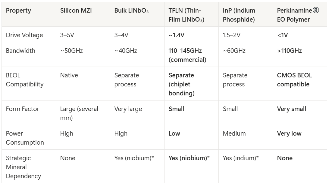
Niobium and indium are not rare-earth elements per IUPAC definition (they are transition/post-transition metals), but both are classified as critical minerals with high China supply chain dependency. LWLG uses “rare-earth-free” in its PR [12], though “critical-mineral-independent” is more scientifically precise.
As the table shows, LWLG’s real competitor is not bulk LiNbO₃ but TFLN. TFLN matches or exceeds EO polymer bandwidth (145GHz for intensity modulators) and achieves a Vπ of ~1.4V. EO polymer’s differentiation comes down to two things: sub-1V drive voltage (even lower than TFLN) and native BEOL compatibility — the ability to spin-on directly in existing SiPho fabs without separate chiplet bonding steps.
Three key points here.
First, sub-1V drive voltage. Conventional silicon modulators need 3–5V; Perkinamine® operates below 1V [11]. This matters because power consumption scales with the square of voltage. In AI datacenters, power is money.
Second, BEOL (Back-End-of-Line) compatibility. Perkinamine® can be “spun on” during the standard CMOS back-end process [11]. No new equipment, no separate fab. For a foundry, this is enormously attractive — just add a process step to your existing line.
Third, no critical mineral dependency. LWLG markets Perkinamine® as “rare-earth-free” [12]. Strictly speaking, the competing materials’ niobium (LiNbO₃) and indium (InP) are not rare earths but critical minerals — yet both carry significant China supply chain exposure. Perkinamine®’s organic polymer structure avoids these dependencies entirely, providing a geopolitical risk hedge.
Commercialization Progress
LWLG tracks its commercialization through a publicly disclosed “Design Win Cycle.” Currently, four Fortune Global 500 companies are in Stage 3 (prototype to final product) [13].
Key milestones:
Nov 4, 2025: First Fortune 500 company enters Stage 3. Additional unnamed foundry secured [14]
Nov 25, 2025: Second Fortune 500 company begins technical program for 400Gb/s CPO with custom Perkinamine® [15]
Jan 12, 2026: Dr. Aref Chowdhury appointed CTO (Nokia Network Infrastructure ($10B revenue) VP Strategy & CTO, previously Nokia Optics CTO) [16]
Jan 15, 2026: MOU with QPICs for EO polymer PDK for quantum processors [17]
Feb 24, 2026: Fourth Fortune 500 company enters Stage 3, targeting 200Gb/s and 400Gb/s [13]
Mar 11, 2026: Tower Semiconductor development agreement for PH18 PDK integration [1]
Here’s where the puzzle clicks. In November 2025, LWLG announced it was adding an “unnamed silicon photonics foundry” beyond its existing AMF collaboration [14]. Today, Tower Semiconductor was formally revealed as a partner [1]. The timeline, context, and technical specs all align — the “unnamed foundry” was almost certainly Tower.
Financial Snapshot
LWLG is still pre-revenue. After completing a $35 million public offering in December 2025, the company holds approximately $70 million in cash [18]. Per the most recent SEC filing (Q3 2025 10-Q), average monthly expenditures are approximately $2.2 million [24] — implying a runway of roughly 2.5–3 years. (Earlier 10-K filings cited $1.7–1.8M/month; the increase reflects rising spend as commercialization efforts accelerate.)
Market cap sits around $630 million [1]. That’s a meaningful premium for a pre-revenue materials company, which tells you the market is pricing in significant commercialization expectations.
Key Takeaway: Perkinamine® has three technical moats: sub-1V drive, BEOL compatibility, and critical-mineral independence. Four Fortune 500 companies are in Stage 3, and the $70M cash position provides ~2.5–3 years of runway.
TSEM × LWLG Agreement — The Core Is PDK Registration
Let me boil today’s announcement down to one sentence: LWLG’s EO polymer modulator just got added to Tower’s PH18 silicon photonics “menu.”
A PDK (Process Design Kit) is essentially a foundry’s catalog of available building blocks. LWLG’s modulators going into the PH18 PDK means that every Tower SiPho customer can now drop EO polymer modulators into their designs without separate material qualification or process development [1]. The adoption barrier lowers significantly. The target specs: 110GHz+ bandwidth, 400G per lane — two to three generations ahead of current commercial silicon modulators (40–50GHz) [1].
What makes this more than a typical MOU, how it fits in the competitive landscape, and what it means for investors is covered below.
TSEM × LWLG Agreement Breakdown — Why This Matters
If you found this useful, please consider subscribing and sharing. The in-depth analysis continues below for paid subscribers.
