
The market read Meta’s move into cloud as a signal of compute oversupply. This piece reads it the other way. As GW grows, the thing that runs short is not the GPU. It is the InP (indium phosphide) laser light source that connects those GPUs. Running compute GW through PhotonCap’s own stress-test model, the contracted compute a single hyperscaler booked in half a year creates InP wafer demand in the same order of magnitude as one full year of revenue capacity at a top-two InP substrate maker. The goal here is to explain that bottleneck with physics rather than tickers, and to walk through the lever of the 6-inch transition, the way CPO raises InP consumption instead of cutting it, and the test bottleneck the market will price in last. Tickers: $AXTI, $COHR, $LITE, $AEHR.
Table of Contents
The market is reading the same compute in opposite ways
Why InP specifically: the material story of the light source
A taxonomy of light sources: why even SiPh needs InP
Translating compute into optics (a stress test)
The real wall is per-lane speed: 200G-per-lane and 1.6T
From scale-out to scale-up: CPO raises InP consumption
The physics of wafer scaling: why 3-inch to 6-inch is the lever
The next bottleneck is test: quieter than CPO, more structural
Paths where this thesis is wrong
Technical implications: who holds the moat
1. The market is reading the same compute in opposite ways
On July 1, when Bloomberg reported that Meta might enter the cloud business (per Reuters) [1], compute-lease names like CoreWeave and Nebius sold off immediately [1]. The overcapacity narrative, “AI compute is heading into oversupply,” came back to life. SemiAnalysis pushed back directly in its July 3 report [2]. Meta’s data center and compute procurement is accelerating, not slowing, and 2027 capex will be “shockingly high.” In the first half alone Meta contracted more than 5GW across Cloud and Colo, and two core campuses account for 2.5GW of capacity under construction [2]. (A “tent-style data center” here means Meta’s ultra-fast buildout style: instead of waiting for a finished building, power, cooling, and compute get pushed into temporary structures to maximize deployment speed.)
I agree with the SemiAnalysis read. A company standing up the cloud capability to resell compute externally is closer to a signal that it expects its own demand curve to keep bending upward. Selling “excess compute” is not evidence of surplus. It is a call option on expanding further in this direction. My read is that Meta widened into cloud because it expects to grow larger here. This pattern is not the first. I covered the case of SpaceX starting to lease compute, where the demand was written directly into the contract (SpaceX Started Renting Out Compute), and Meta is closer to the second signal following it.
SpaceX Started Renting Out Compute. The Rig Demand Is Now Written Into the Contract.

The copper in NVL72 did not kill optical demand. The market was looking inside the rack. The money is outside it. When NVIDIA wired its 72 GPUs together over an NVLink copper spine, a bear case followed: maybe optical content shrinks. That is the read SemiAnalysis called the “optical boogeyman.” But it treats scale-up and scale-out as the same network, …
If that view is right, the recent market reaction was a misread. Overcapacity fear pressed on memory-linked names and parts of the AI-infrastructure trade, but if real demand is accelerating, that correction was a mispricing and an opportunity, in my judgment (the investment call is yours). And when data centers grow, the benefit does not stop at memory. Hardware broadly benefits, and the optical interconnect that physically links that hardware benefits structurally. The catch is that this optical interconnect layer is the most supply-constrained of all.
Memory and optics are really two faces of the same wall. As I covered in The More Anthropic Buys Micron HBM, the Faster Optical Memory Pooling Arrives, the way HBM solved the memory wall was proximity, putting memory right next to the GPU, and that proximity becomes a capacity ceiling. The moment you try to detach and pool capacity, distance becomes a wall again, and crossing that distance without bandwidth or latency loss is exactly what optics does. So the stronger the electrical HBM contracts get, the greater the pressure to detach capacity cheaply (memory disaggregation), and two of the three paths for that are optical. Accelerating compute creates bottlenecks in memory and optics at the same time.
The More Anthropic Buys Micron HBM, the Faster Optical Memory Pooling Arrives

On June 22, 2026, Micron ($MU) announced a strategic agreement with Anthropic bundling a memory supply contract, joint design work, and a strategic investment into Anthropic’s Series H round [1]. Around the announcement, the stock traded at record-high levels [2]. Yet read the full agreement and the words optical, photonic, and interconnect never appear…
The same house’s analyst Konrad Wang framed InP as “one of several supply bottlenecks collectively gating the AI data center buildout” (Reuters) [3]. The bottleneck that links compute is not the GPU. It is the laser light source that makes the light. And that laser is mostly built on InP, a compound semiconductor that neither silicon nor GaAs can fully replace. The more tents Meta pitches, the faster InP runs dry. Start with why InP specifically.
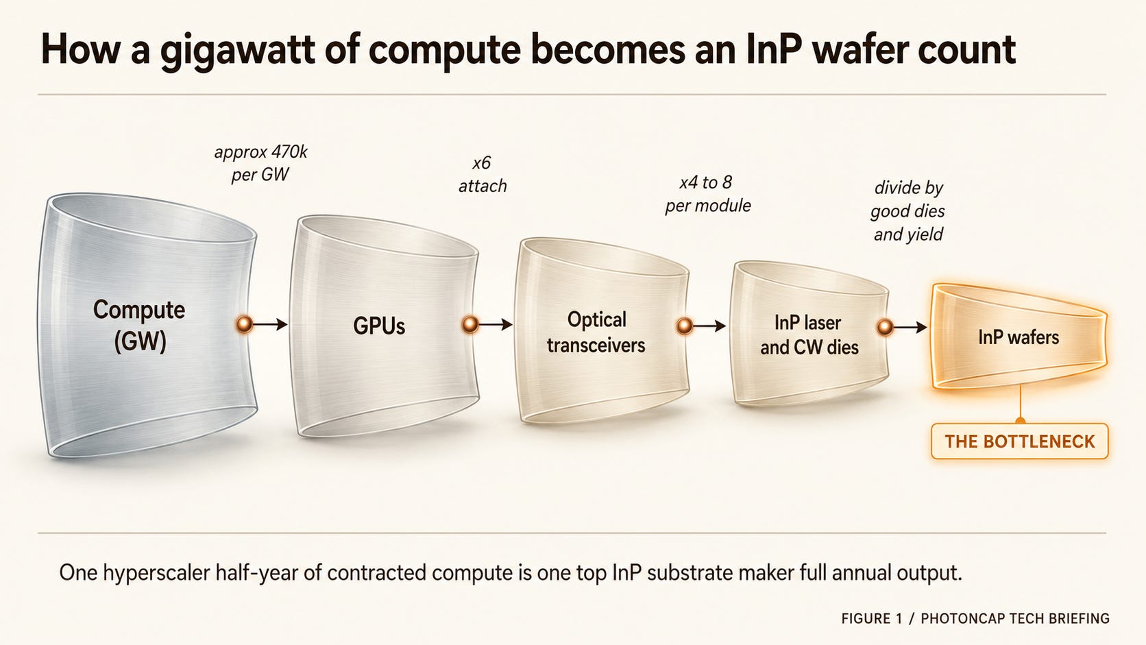
Figure 1: Compute GW to InP wafer translation chain
Figure 1. GW to GPU to optical transceiver to InP laser/CW die to InP wafer. Each stage multiplies the one before it, and the chain condenses into a compound-semiconductor bottleneck. (Quantitative model in Section 4.)
2. Why InP specifically: the material story of the light source
The semiconductor that makes light and the one that does computation want different band structures from the start. Silicon is an indirect-bandgap material. When an electron drops from the conduction band to the valence band, the momentum does not line up, so the energy leaves as lattice vibration (heat) rather than a photon. That makes silicon an excellent transistor and a poor light emitter. At the research level there is active work to put quantum-dot lasers or III-V bonded and heterogeneously integrated light sources on silicon, but commercial datacom silicon photonics (SiPh) still depends on an external III-V source for the light itself.
InP is the opposite. It is a direct-bandgap material, so electron-hole recombination comes straight out as a photon. On top of that, the InGaAsP and InGaAs active layers lattice-matched to InP operate exactly in the key optical-communication bands (1310nm O-band, 1550nm C-band). Those two wavelengths matter because the loss and dispersion of silica fiber are optimal there. It is a material where the communication wavelengths and the band structure happen to line up. Add high electron mobility and you get ultra-high-speed modulation.
So InP is effectively impossible to replace commercially in the near to mid term. GaAs-based VCSELs pull 850 to 940nm cheaply, but the wavelength is off, so they cannot be the default for medium and long-reach datacom scale-out, and even SiPh depends on an InP CW source for its light. That is why industry contacts and SemiAnalysis alike describe it as “a material with no commercial drop-in substitute” [2]. On top of that, switching an InP substrate supplier typically requires 12 to 24 months of engineering validation and qualification, so even if an alternative source exists, you cannot swap it in overnight. It is a double bottleneck: the necessity of the material itself, layered with the rigidity of the supply chain.
3. A taxonomy of light sources: why even SiPh needs InP
The light sources you build on InP are not one kind either. The device structure splits based on how the transceiver puts light on the wire.
The EML (electro-absorption modulated laser) integrates a CW-emitting DFB laser and an electro-absorption modulator (EAM) on a single InP chip. Having the source and modulator in one body helps with speed and miniaturization, but that makes the epitaxy and process demanding. So the number of makers volume-producing 200G-per-lane class EMLs is small (Lumentum, the Coherent family, Mitsubishi, and a few others). Add the InGaAs photodiode (PD), which is also usually built on InP-family epitaxy. EML, CW laser, and PD all sit on the InP substrate and epi ecosystem, so the bottleneck condenses into this one upstream spot.
The CW (continuous-wave) laser is a source that supplies pure light with no modulation. And this CW laser is both the Achilles heel and the lifeline of silicon photonics. SiPh does modulation, routing, and even multiplexing in silicon waveguides, but in commercial datacom it cannot make the light. So a SiPh transceiver has to attach an external InP CW laser as its source to work. Against the common belief that “SiPh replaces InP,” the more commercial SiPh spreads, the more InP CW laser demand rises with it. Silicon does not push InP out. It lives on top of InP.
The economics of these two explain why SiPh keeps getting used more. As I noted in The AI Light Source War Is Not a Winner-Take-All, an EML-based 800G module uses eight 100G EMLs, so laser cost alone lands roughly in the $80 to $100 range per module, while moving the CW laser outside and handing modulation to a SiPh chip cuts the sources to two to four and brings that down to the $20 to $40 range (industry estimate). This structural cost gap is what keeps pulling SiPh adoption up, and at the same time it supports InP CW source demand from below. The choice to lower cost pushes the bottleneck into deeper upstream.
The AI Light Source War Is Not a Speed Race: InP, VCSEL, and μLED Are Buying Different Distances

When PicoJool unveiled its 200G VCSEL and 32x50G μVCSEL on June 15, 2026, a 30-year-old technology landed back on the table as an AI data center light source candidate [1][3]. Around the same window, Avicena, back in the spotlight before and after the PicoJool news, was pushing a non-laser GaN μLED link, driving Tx energy from 200fJ/bit in September 2025 down to 80fJ/bit in November 2025 [4][8]. Data center light sources are now splitting into three material systems and structures: InP edge-emitting laser, GaAs VCSEL, and GaN μLED. But the question the market asks, “who builds the faster laser,” is not the real one. The real axis is which light source the reach, lane count, and serialization cost actually call for. This piece lays out the physics of the three, then uses two axes, “fast and narrow” and “slow and wide,” to map which source takes which seat and which companies already sit there. Related tickers: $AAOI, $LITE, $COHR, $SIVEF, $ALMU, $AVGO.
To sum up: VCSEL (GaAs) is short links, EML (InP) is a source-and-modulator combo, and CW (InP) plus SiPh is the architecture where silicon does the modulation and InP supplies the light. Whichever path you take, the light-source seat for medium and long-reach data center optics stays with InP. This device diversity actually reinforces the InP upstream bottleneck.
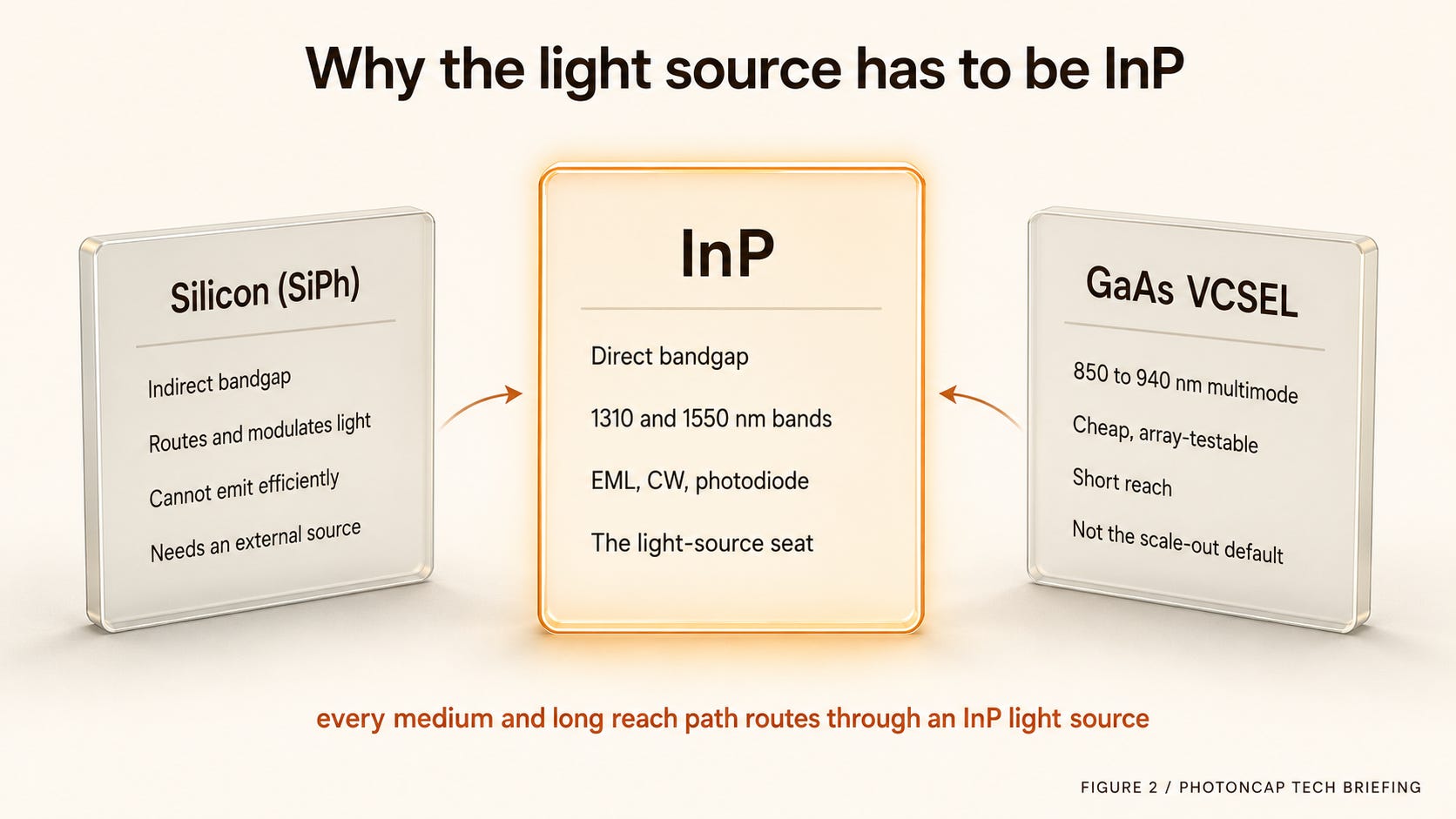
Figure 2: Why the light source has to be InP
Figure 2. Silicon routes and modulates light but cannot make it, and the GaAs VCSEL stays short-reach. Medium and long-reach datacom converges on an InP source.
This is where the free portion ends
So far I have used physics to pin down why InP is the material root of the optical bottleneck. From here, subscriber-only:
PhotonCap’s own stress-test model translating GW into InP wafers (Meta 5GW = one substrate maker’s annual capacity)
The real wall of 200G-per-lane, why CPO raises InP instead of cutting it, and the physics of the 6-inch transition
The next bottleneck the market has under-priced: test (ATE), the one I hold most strongly
Falsification scenarios and a tracking map
Related PhotonCap reading
AXT (AXTI) Deep Dive: InP, the Hidden Bottleneck of AI Optical Interconnect, the substrate layer of this piece
Everyone Saw a Laser Shortage. The Money Went to the Foundry First, SiPh foundry, InP, and SOI capacity
The AI Light Source War Is Not a Winner-Take-All, narrow and fast vs wide and slow
Compute Is the New Oil: So Who Builds the Drilling Rigs, the supplier-agnostic test and equipment layer
The Three Pillars of SiPh Wafer Test: AEHR, FORM, KEYS, the test bottleneck in Section 8
SpaceX Started Renting Out Compute: Demand Written Into the Contract, the macro precedent in Section 1
