
The Three Pillars of SiPh Wafer Test: What AEHR, FORM, and KEYS Actually Do
What Teradyne’s Photon 100 announcement confirms about the test equipment ecosystem, and where the market goes from here

Abstract
NVIDIA’s string of multibillion-dollar investments in Lumentum, Coherent, and Marvell over the span of a single month signals that the SiPh optical interconnect supply chain is moving into serious production mode. Before any of those wafers can go into CPO packaging, they have to pass wafer-level test (WLT). On March 17 at OFC, Teradyne introduced the Photon 100, a purpose-built integrated ATE for SiPh. A natural question for any investor: does this threaten the existing SiPh test equipment players? This article answers that question directly. The SiPh WLT ecosystem is divided into three non-overlapping roles: burn-in screening (AEHR), wafer optical probing (FORM), and optical measurement (KEYS). Photon 100 is not a competitor to any of them. It fills a position that did not previously exist. And when you consider where Teradyne sits in the broader semiconductor ATE market, this move carries a structural message for the entire SiPh test ecosystem.
Contents
Why SiPh Testing Is So Demanding
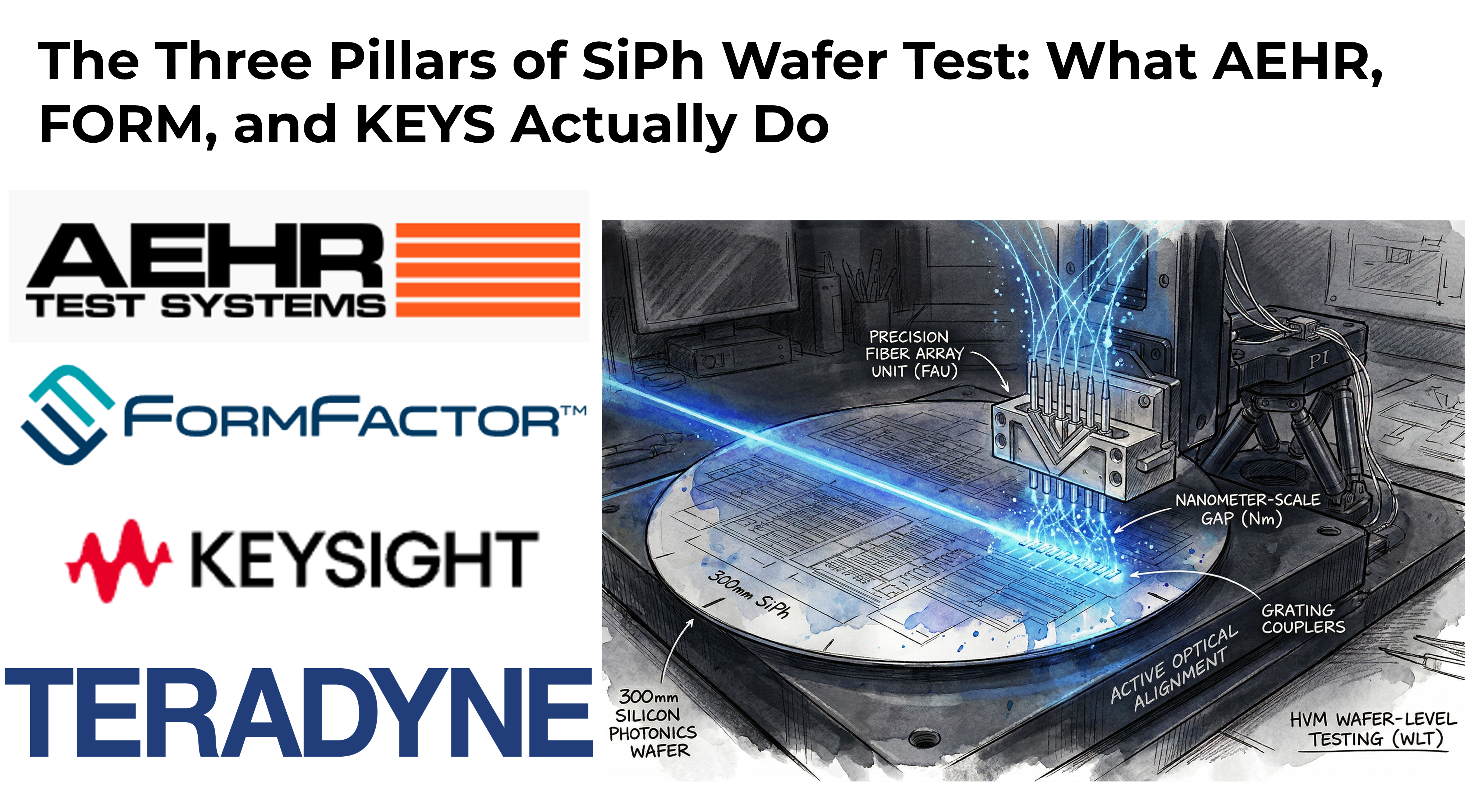
The Three Pillars: AEHR, FORM, and KEYS
Aehr Test Systems: Burn-In Screening
FormFactor: Wafer Optical Probing
Keysight Technologies: Optical Measurement
Teradyne Photon 100: What the Announcement Actually Means
Summary: The Three Companies
How Big Is This Market, and How Does It Grow
Closing
NVIDIA announced three optical partnerships in the span of a month.
On March 2, it announced strategic partnerships with both Lumentum (LITE) and Coherent (COHR), investing $2 billion in each alongside multi-year purchase commitments.[1] On March 31, it added Marvell (MRVL) to that list, again with a $2 billion investment.[2] The Marvell announcement explicitly includes joint development of “optical interconnect solutions and silicon photonics technology” on top of the NVLink Fusion-compatible custom XPU collaboration.
NVIDIA's $4 Billion Photonics Bet: Broadcom Wasn't Wrong — But the Market Completely Misread the Signal

1. Introduction: The Announcement and the Market’s Reaction
All three partnerships point at the same thing: SiPh-based optical interconnects as the backbone of next-generation AI infrastructure. Lumentum and Coherent now need to produce lasers and optical components at scale, and every one of those wafers has to pass test before it goes anywhere near a CPO package. You cannot secure Known Good Dies (KGD) without wafer-level test.
So who does the testing?
This article covers the three companies that own the SiPh wafer test ecosystem. It also breaks down what Teradyne’s (TER) Photon 100 announcement actually means for them, and where the market goes from here.
1. Why SiPh Testing Is So Demanding
CPO integrates GPU dies with Photonic Integrated Circuits (PIC) into a single package. If a defect shows up after packaging, you scrap the entire module, which can run thousands of dollars. Securing KGD before packaging is not optional; it is the entire reason WLT exists.
Two specific challenges make SiPh WLT uniquely difficult.
First, the compound semiconductors used as light sources, particularly Indium Phosphide (InP)-based laser diodes, are highly vulnerable to thermal degradation. Burn-in testing, applying concentrated electrical and thermal stress to screen out early failures (infant mortality), is mandatory.
Second, aligning a Fiber Array Unit (FAU) to the grating couplers on the wafer surface requires nanometer-level precision. FAU coupling efficiency is a determining factor in SiPh device performance,[3] and even slight misalignment produces insertion loss. Automating this alignment at production scale is the single biggest bottleneck in SiPh high-volume manufacturing.

Two core challenges for SiPh WLT: burn-in screening for compound semiconductors, and automating nm-level optical alignment.
2. The Three Pillars
The SiPh WLT line breaks into three distinct layers. Each has a dedicated player, and none of them overlap.
Aehr Test Systems (AEHR): Burn-In Screening
Aehr Test Systems is a pure-play wafer-level burn-in (WLBI) company.
InP-based laser diodes are susceptible to both electrical and thermal stress. The goal of burn-in is to apply that stress early and hard, forcing weak devices to fail before they reach packaging. Doing this at the wafer level, before individual die separation, is what WLBI is about. The cost of discovering a defective laser after it has been packaged into a CPO module is far higher than catching it at the wafer stage.
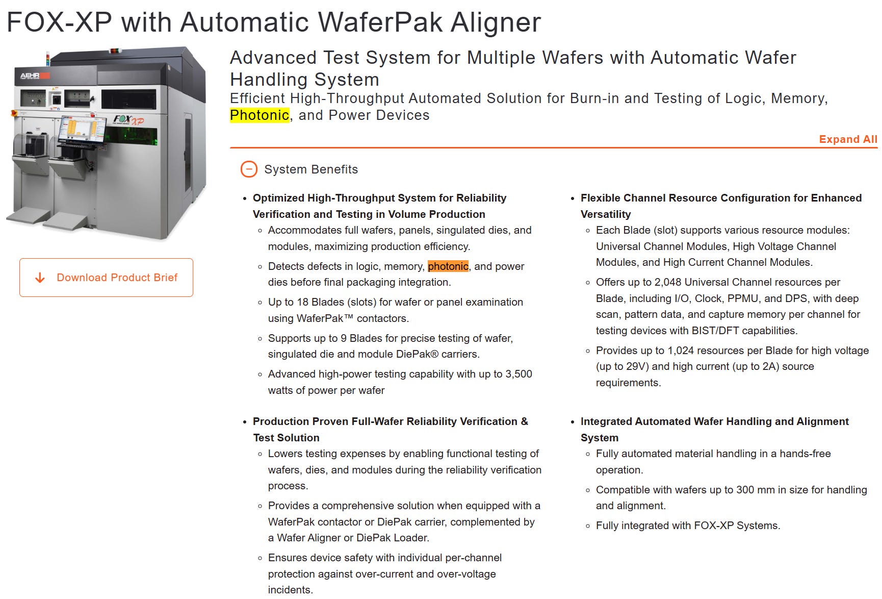
Aehr’s core platform is the FOX-XP, capable of applying up to 3,500 watts per wafer in a high-power burn-in configuration while processing nine wafers in parallel. That high-power FOX-XP configuration is already installed and running in production at a world-leading SiPh IC supplier.[4]
On March 31, the same day as the NVIDIA-Marvell partnership announcement, Aehr disclosed a significant new customer win. A major new customer described as a global leader in networking products and a major supplier to the data center optical transceiver market placed an initial order for SiPh WLBI systems.[4] The customer is developing SiPh-based transceivers and Optical I/O products for hyperscale AI and cloud data center deployments. The order covers a FOX-XP system configured for nine wafers in parallel, a WaferPak Auto Aligner, multiple FOX-NP systems, and full production sets of WaferPak Contactors. Shipment is scheduled within Aehr’s fiscal Q4 ending May 29, 2026. The customer has already provided a forecast for additional systems, with follow-on orders possible as early as later this calendar year.
Aehr CEO Gayn Erickson highlighted that the customer purchased systems for both engineering qualification and high-volume production upfront, which reflects the urgency of the ramp already underway. As SiPh laser wafer production volumes increase, WLBI demand follows directly.
FormFactor (FORM): Wafer Optical Probing
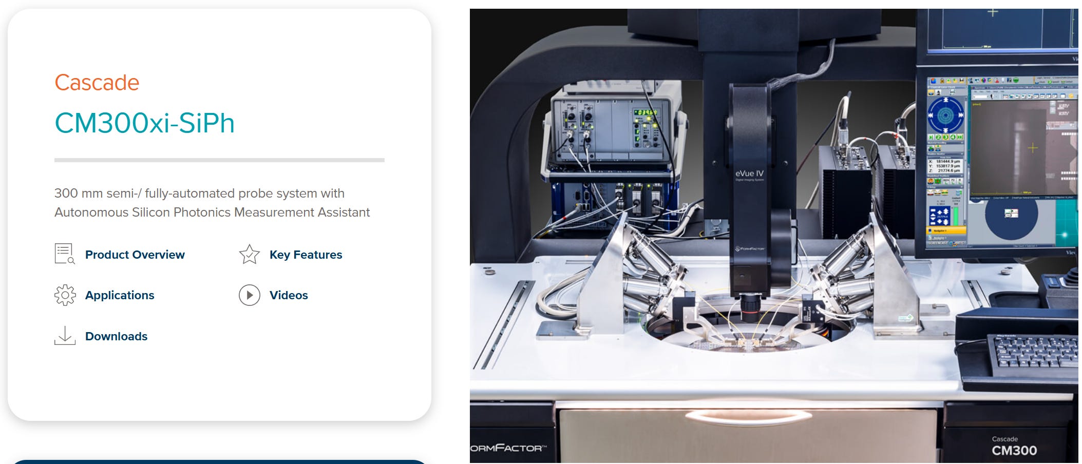
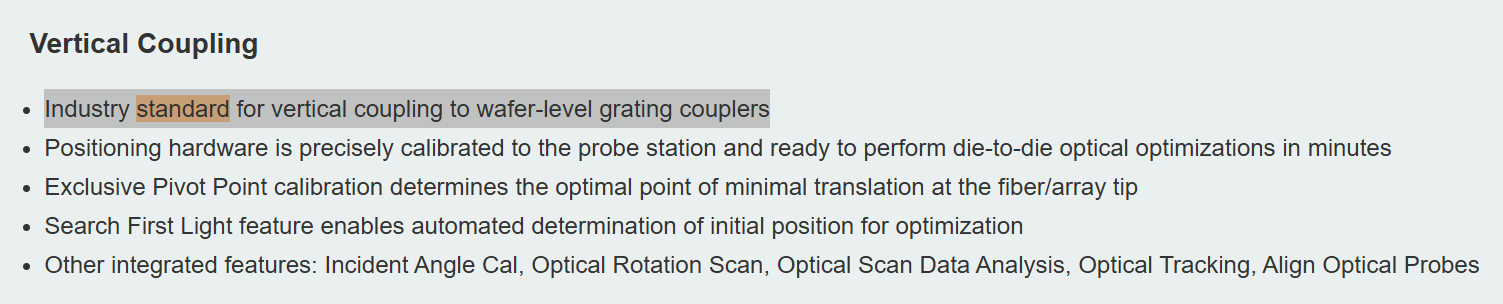
FormFactor is the industry standard for SiPh wafer probing. Its distributor PSI Solutions lists the CM300xi-SiPh as the “Industry standard for vertical coupling to wafer-level grating couplers,”[5] and the system is currently in use at over 100 leading SiPh device manufacturers worldwide.[6]
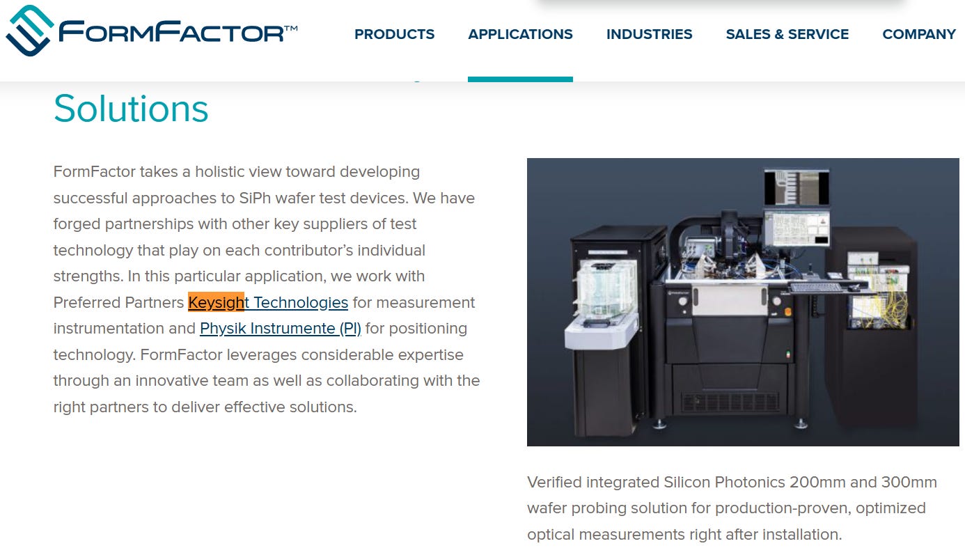
The CM300xi-SiPh has a six-axis precision hexapod motion stage from Germany’s Physik Instrumente (PI) built directly into the system.[7] This handles the active alignment of the FAU to the wafer’s grating couplers at nm-level precision. FormFactor’s official documentation lists both PI (positioning) and Keysight Technologies (measurement instrumentation) as “Preferred Partners” for SiPh WLT,[8] which tells you a lot about how the ecosystem is structured.
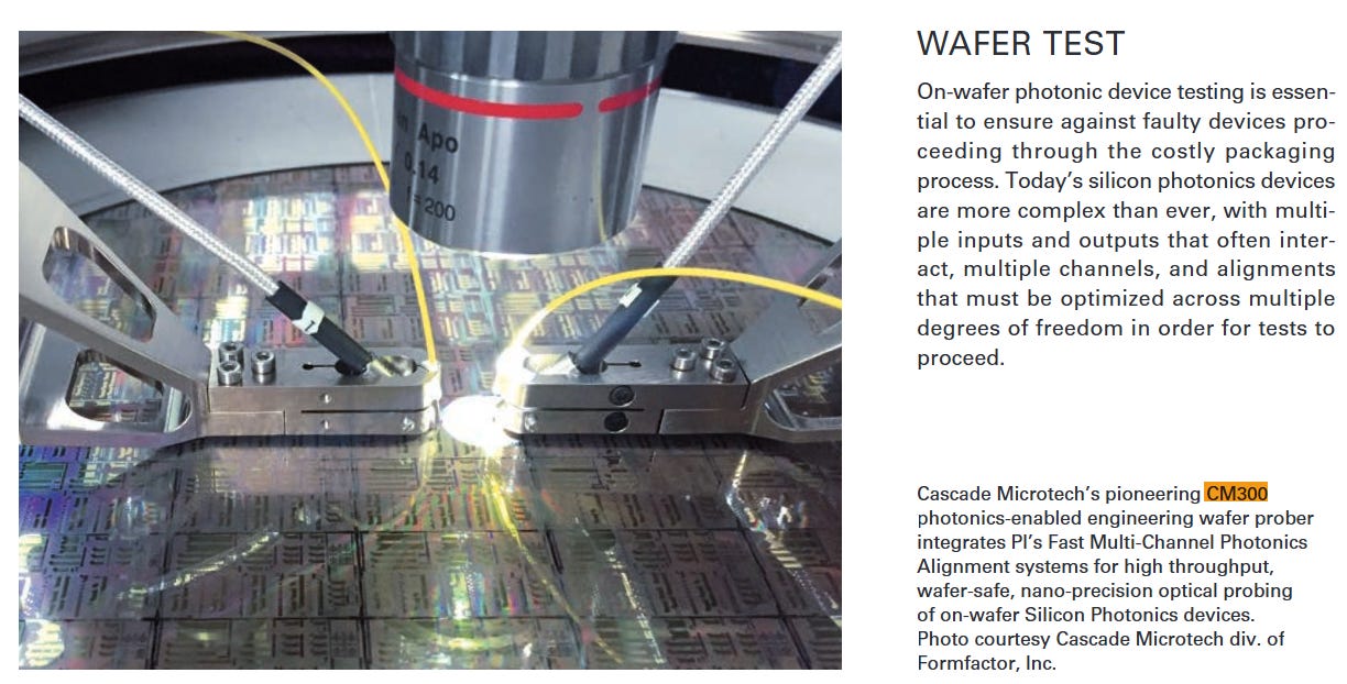
On top of the PI hexapod, the system ships with the Pharos probe card,[9] SiPh-Tools software, and the OptoVue autonomous calibration system, all packaged into a solution that is ready for production measurements immediately after installation. FormFactor’s own description: “first verified integrated measurement solution on the market that enables engineering and production-proven, optimized optical measurements right after installation, without further development.”
In December 2025, FormFactor acquired Keystone Photonics, a specialist in optical coupling technology for SiPh probing.[10] Management described the acquisition as reinforcing their “lab-to-fab” position, meaning test continuity from early R&D through high-volume production.
Keysight Technologies (KEYS): Optical Measurement
Keysight handles the optical measurement side as FormFactor’s official Preferred Partner, supplying the instruments that actually send and receive optical signals and extract measurement data.[8]
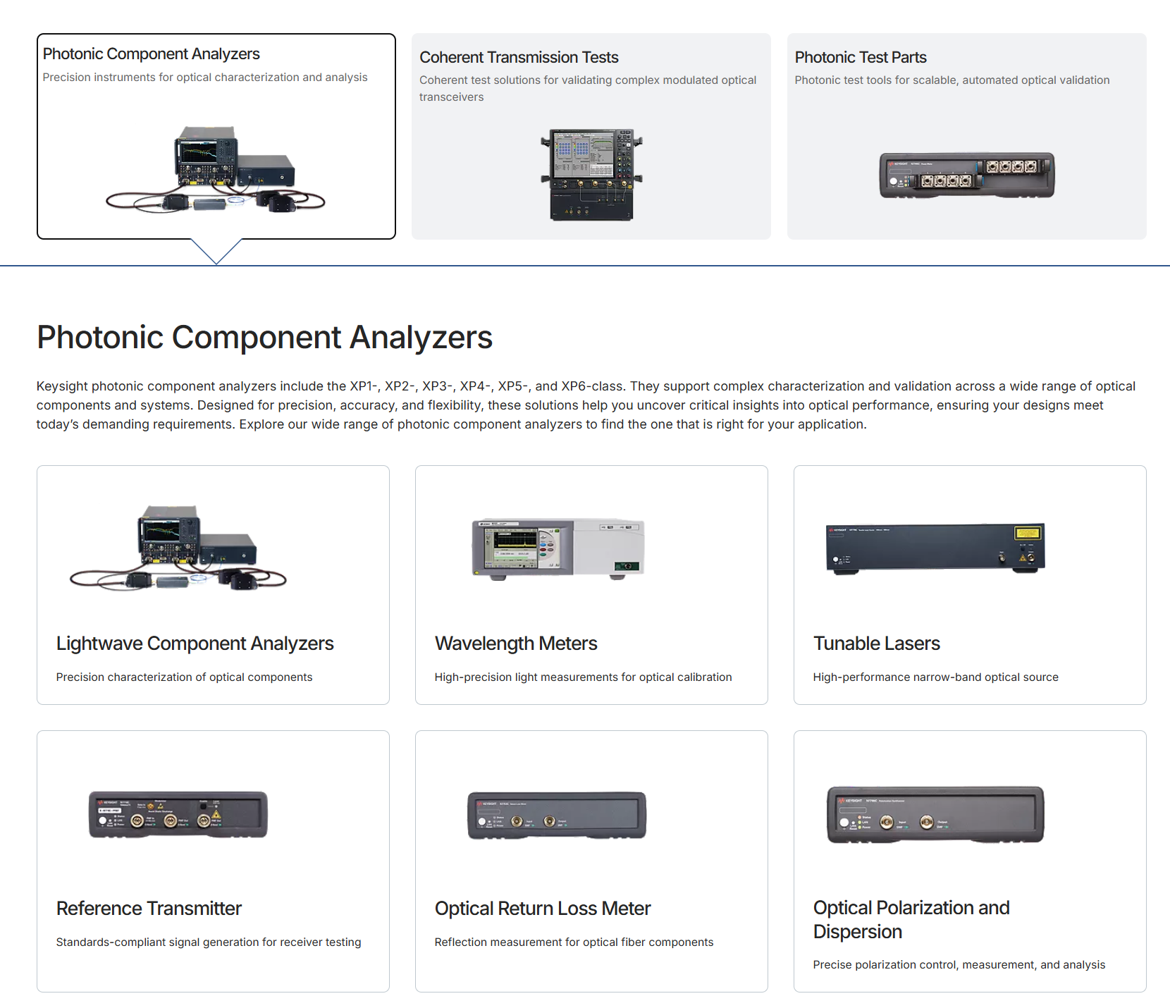
At the wafer level, that means Tunable Laser Sources (TLS) and Power Meters (PM) for measuring insertion loss (IL) and polarization-dependent loss (PDL), alongside Optical Spectrum Analyzers (OSA). At the package and module level, it means BERTs and oscilloscopes for verifying the signal integrity (SI) of 800G and 1.6T transceivers.
Historically, customers buying CM300xi-SiPh systems sourced these instruments separately, integrated the software themselves, and maintained the multi-vendor stack on their own. That worked well enough in engineering environments. At HVM scale, that integration burden becomes a production bottleneck.
