
In my January 26 article, I wrote that HBF (High Bandwidth Flash, NAND stacked like HBM) was likely to pull optical interconnect demand forward. Eight months later, on September 18, I heard about HBF and microLED optical links firsthand at the packaging roundtable of the SK hynix Global Forum, and it was far more reserved than I had expected. HBF and microLED are both cards the memory side played first, yet on the packaging side the temperature was lukewarm for both. Meanwhile, things outside were fairly busy. Sandisk said HBF customer samples would come next year, and at Hot Chips the takeaway that HBF belongs in the box rather than the rack came from Sandisk’s own advisory circle. Micron put its name down as a supplier for the first time with NVHBM, the custom HBM4E it co-designed with NVIDIA, and a joint venture set up by Wuhan’s Jiufengshan Laboratory (JFS) wrote microLED optical interconnect into its business scope. Following them one by one, I could see that HBF and microLED are stuck at the same spot, and my lead is that the spot is the land on the SoC edge more than the technology, and that Micron’s NVHBM, which a subscriber asked about, is the first product to touch that land.
Contents
Asking About HBF
The Record from the Past Eight Months
The Land on the SoC Edge (Paywall)
Where Optics Comes In
Checking the January and August Articles
Closing
References
1. Asking About HBF
If you only follow the HBF news, the past eight months were quite busy. But who will actually use this memory, and where, is hard to find anywhere in the public record. At the packaging roundtable of the SK hynix Global Forum, held in the US on September 18, I got to hear an answer to that blank firsthand.
Late in the Q&A, after the speaker described a picture with high-stack HBM or HBF placed next to DRAM on logic, the talk moved on to HBF. The speaker began with the caveat of not being an architecture person. Then came the answer: customers also don’t seem to have decided yet in what form they would use HBF, the HBF concept didn’t come from the customer side so there is no killer application yet, and that is why the company is taking part in a consortium to discuss which platform to go with.
Earlier in the same roundtable, HBF had been introduced from the technology side. The basic frame is the same as HBM, and the biggest difference is that the chips being stacked change from DRAM to NAND, the speaker said. Today’s NAND is built by making the peripheral circuit wafer and the cell wafer separately and bonding them together, so the key question, the explanation went, is whether that structure holds up when many of them are stacked. In a word, it is memory with HBM-like bandwidth and SSD-like capacity, but making it work properly across a whole system is not easy, the speaker said. The order I heard then was that the company is preparing validation internally, and once the technology works, it will run system-level validation with customers in the form of a PoC (proof of concept).
The point that the concept came first from the supply side rather than from customers came up once more the same day in a different context. Asked what “memory-centric” means, the speaker said that in the past system makers defined memory functions and brought them as specs, but now even they can’t define them, and that HBF too was something SK hynix brought up first. The speaker offered this less as a weakness than as an example of an era in which memory companies have to design first and propose. So reading “customers haven’t settled on where to use it” as a declaration that HBF has failed would be an overreading.
The HBF and microLED I saw and heard at the venue were, in fact, below expectations. It didn’t feel very proactive. Looking back, it wasn’t surprising. The standard was coming out fast, but no company name ever showed up saying it would use it, and that had kept bothering me. Still, I’m the one who tied HBF to optical demand in January, so after hearing this answer I had to look at that link again first.
This event was an invitation-only gathering that doubled as recruiting, so I didn’t receive the presentation materials. As with Parts 1 through 3, numbered facts were checked against public sources, and things I only heard on site are marked as such. The first three parts followed the packaging talk I heard at the same event in order: the map, sideways, and upward.
Part 1, SK hynix’s Four Packaging Paths: Where Is the Fight After HBM?: a map of the four paths SK hynix packaging is branching into, and where the fight goes after HBM
Part 2, SK hynix’s In-House 2.5D: Validation Comes Before Commercialization: why a memory company builds CoWoS-class 2.5D itself, read as validation more than as a business
Part 3, SK hynix’s DRAM on Logic: Who Stacks It, and Who Buys the Bonders?: with DRAM bonded on top of a logic chip, who stacks it and who buys the bonders
This bonus part covers the HBF and optical interconnect talk from the same roundtable.
2. The Record from the Past Eight Months
When I wrote HBF (High Bandwidth Flash) and Optics: The Missing Link in AI Infrastructure on January 26, HBF was at the level of conference papers and concepts. I laid out the public record that has piled up since, in date order.
The starting point is the August 2025 standardization MOU between Sandisk and SK hynix. At the time, Sandisk said it aimed to deliver first HBF samples in the second half of 2026 and samples of the first AI inference devices with HBF in early 2027 [1]. In February this year a standardization consortium launched and a dedicated workstream was set up inside OCP (Open Compute Project, a body where hyperscalers turn hardware specs into open standards) [2], and the first technical specification came out at FMS in August. It allows up to 512GB per stack with 8-high and 16-high NAND, bandwidth in three grades from 0.4TB to 3.0TB per second, and a connection to the processor through UCIe, the standard chiplet interface [3]. The consortium members announced then were Google and Tenstorrent [4], and ten days later Meta’s joining was disclosed at Sandisk’s investor day [5][6].
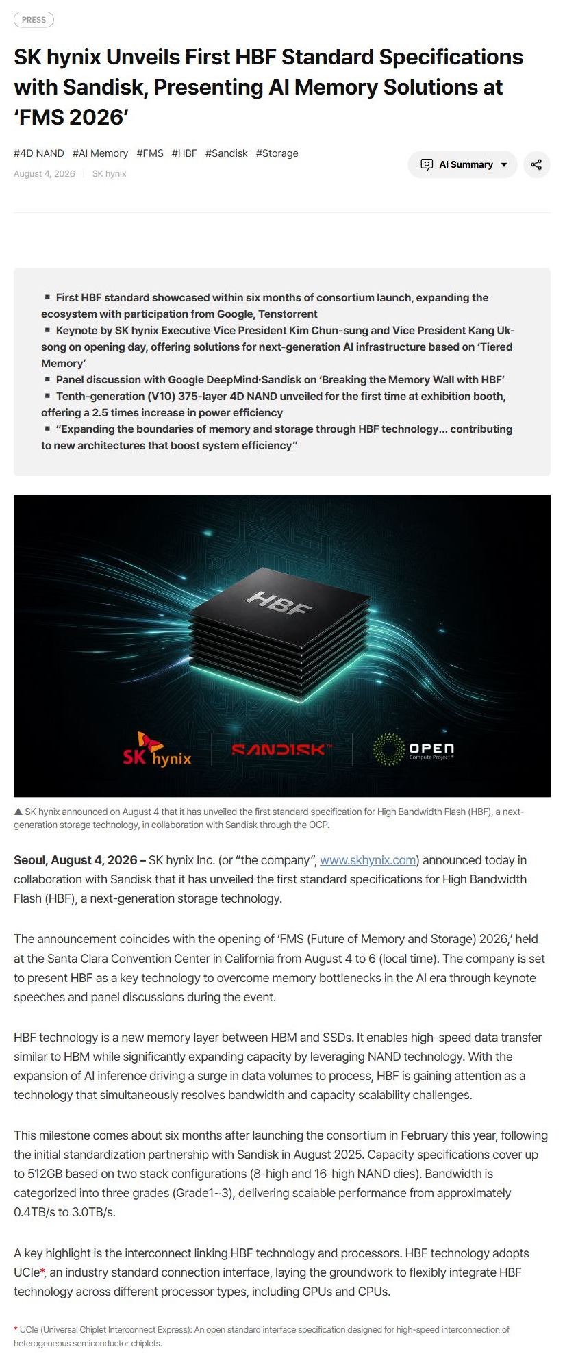
SK hynix Newsroom announcement of the first HBF standard specification at FMS 2026 (up to 512GB per stack, three bandwidth grades, UCIe)
The schedule moved a bit differently. At the same investor day, Sandisk reportedly said it had finished the tape-out (the stage where design is done and handed over for production) of its first HBF die and that customer samples would come next year [6]. A year earlier the target was first samples in the second half of 2026, and this time the wording was customer samples in 2027, so it isn’t clear whether the two refer to the same samples. Still, going by when customers get them in hand, it has become 2027. The sentence that sets the clock even longer comes, if anything, from SK hynix. The newsroom post announcing the consortium launch in February wrote that the industry expects demand for composite memory solutions including HBF to take off around 2030 [2]. At AI Infra Summit in mid-September, SK hynix introduced HBF as a next-generation NAND solution that applies TSV (through-silicon via, a vertical electrode cut through the silicon) like HBM, but it gave no specs or schedule [7].
To square this ledger, I put the MOU press release from a year ago next to the August spec release and looked for the schedule sentence, and the August release had no schedule sentence at all.
There are no named customers yet. Google and Meta are members helping write the spec, and neither has been announced as a buying customer. In late August, NAND Research noted that NVIDIA, AMD, Intel, Broadcom, Marvell, Micron, Samsung, Qualcomm and Western Digital had not joined the consortium, and that the standard is therefore not currently supported by merchant GPU vendors [8].
Records on the other side piled up too. At Hot Chips in August, OXMIQ Labs showed a calculation running the Kimi-K2 model on a 72-GPU rack: at the same cost and power, using only HBF instead of HBM raises capacity by a whopping 14 times, to nearly 300TB, but cuts the rack’s total bandwidth by a little over 40 percent compared with HBM only [9][10]. It also attached conditions, that there is no software support yet and that reads and writes have to happen in large units, and the conclusion was reportedly to put HBM in the rack and HBF in the box [9]. OXMIQ founder Raja Koduri is listed on Sandisk’s HBF technical advisory board in its investor day materials [5]. So this takeaway is closer to a usage map drawn inside the same camp than to outside criticism. NAND’s write endurance keeps coming up as well. One analysis says the KV cache (memory that holds the conversation context), which has to be written anew for every token generated, is more than NAND’s write endurance can handle, so HBF belongs with model weights [11]; there is also an opposing view that the KV cache is mostly reads [12], so where HBF fits best is not settled yet.
That was a long stretch, but if I shrink the ledger to one line, the spec and the consortium came faster than expected, while customers and schedules are coming about a year late. The roundtable answers pointed the same way as this ledger. What I gained on site beyond that was that the temperature was a notch lower than the public record alone would suggest.
Up to here is where the public record and the on-site answers overlap. But at the end of the same answer, the speaker added one more technical reason, and that reason wasn’t a problem for HBF alone. In the paid section I go on to why that reason is a problem of land on the SoC edge, and why a question from the subscriber chat, “What do you think of Micron’s new product?”, is exactly about that land. The on-site answer on microLED optical links, another subscriber’s question asking me to watch Wuhan’s JFS, and the check against my January and August articles come after that.
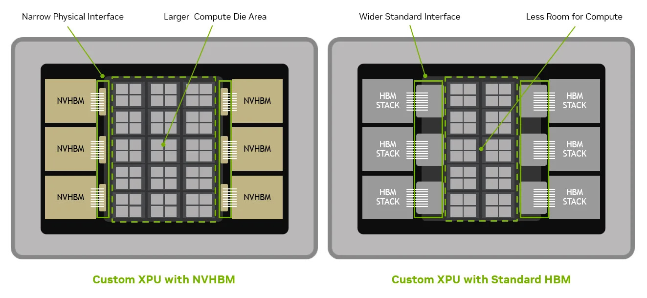
NVIDIA’s NVHBM comparison. NVHBM on the left, standard HBM on the right; with NVHBM the physical interface on the XPU die narrows and the compute die area grows
