Price and market cap data as of the September 18, 2026 close (TradingView, retrieved September 20)
TL;DR
SK hynix is the HBM leader and its stock is up more than fivefold in a year. Yet at a roundtable of the company’s Global Forum in the US on September 18, a packaging development executive said there isn’t much time left to get by on memory packaging technology alone, and I took him at his word.
The reason he says so is that the three walls, scaling, memory, and heat and power, are really one problem. Push bandwidth and power goes up, push power and heat goes up, and making devices smaller can no longer break that loop.
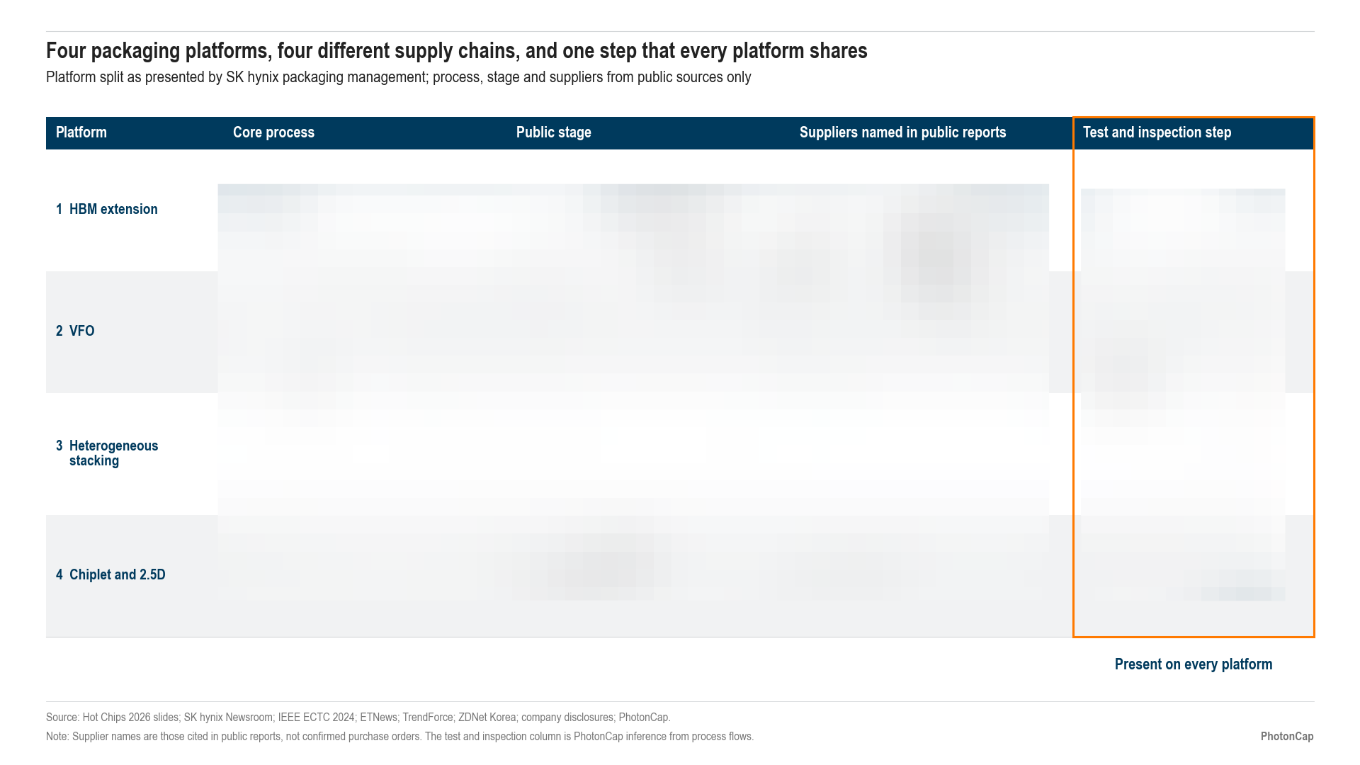
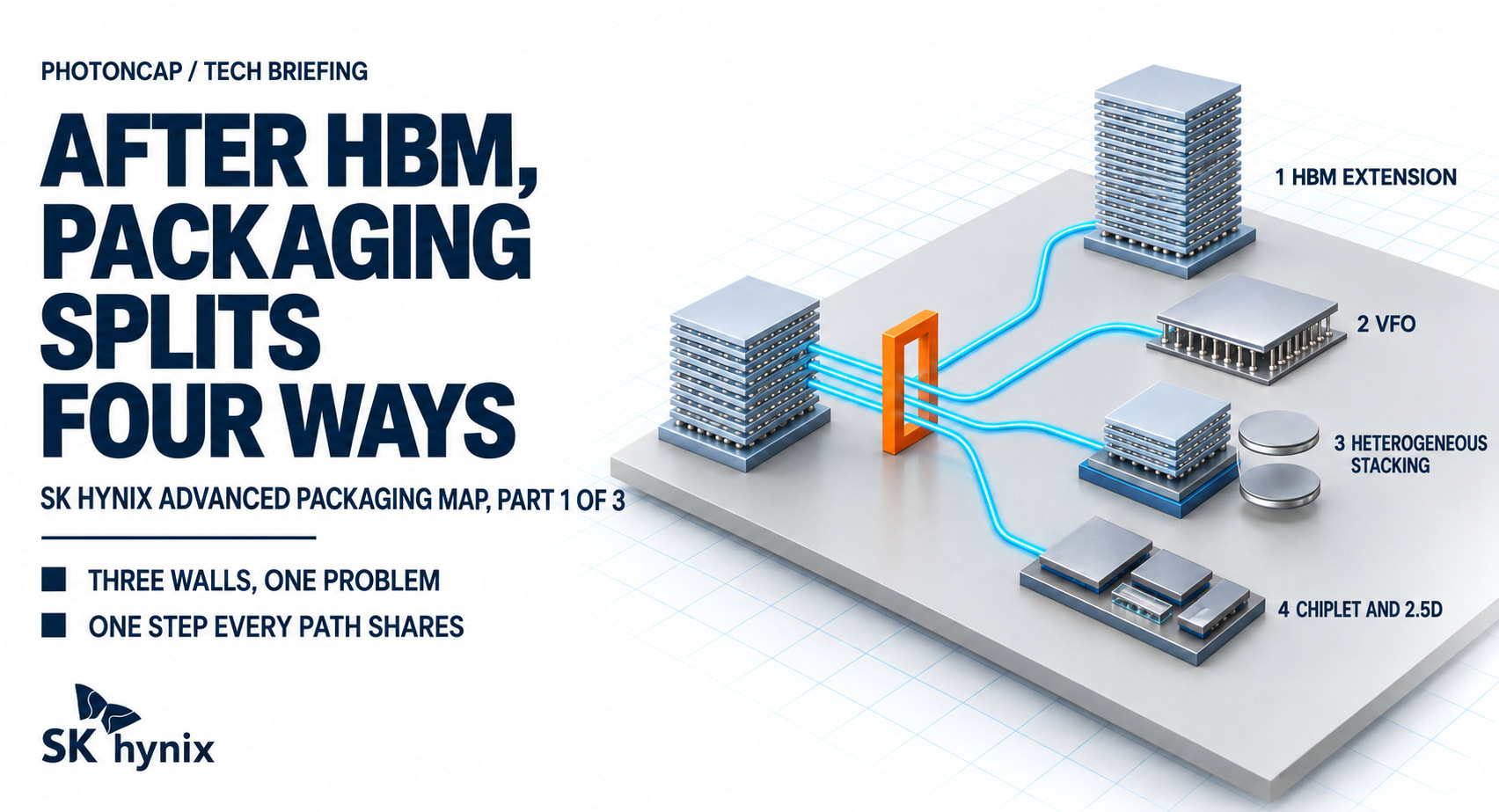
So gaps open in the memory hierarchy, and packaging splits four ways to fill them: HBM extension, VFO, heterogeneous stacking, and chiplets with 2.5D. The fight after HBM happens in packaging platforms more than in memory chips.
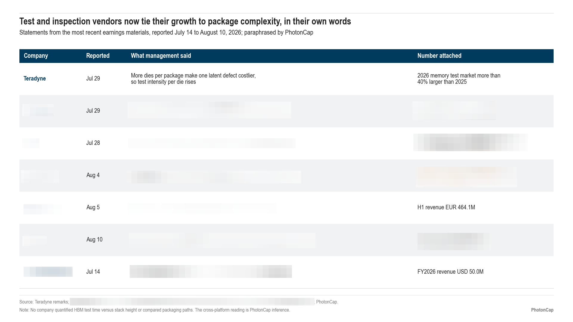
While matching the listed suppliers of each path against filings and earnings materials one by one, interestingly, I think I found something. Korean companies that all get filed under “test and inspection” posted opposite results in the second quarter.
My lead: whichever of the four paths wins, you still have to screen parts before you bond them, so the money goes to test and inspection first.
Contents
The Roundtable on the Afternoon of September 18
The Three Walls Are One Problem
The Gaps in the Memory Hierarchy
The Four Path Map (Paywall)
Which of the Four Comes First
Where the Money Goes: Test and Inspection
Same Test and Inspection, Different Second Quarter
Closing: Base, Alternative, Downside
References & Sources
1. The Roundtable on the Afternoon of September 18
SK hynix shares have risen more than fivefold over the past year. At the September 18 close its market cap sat in the $970 billion range, with $1 trillion in sight [1]. Few would argue that this is the number one company in HBM (high bandwidth memory, the AI memory made by stacking DRAM dies vertically and placing them right next to the GPU).
From a packaging development executive at that company, I heard in person that there isn’t much time left to get by on memory packaging technology alone. It was at the afternoon roundtable of the Global Forum SK hynix held in the US on September 18. It was a recruiting event, so I went in casually, but the afternoon roundtable turned out to be the most technical session of the day. The talk ran under 40 minutes and the questions went on for more than an hour. They never stopped.
Everyone seemed unsure what to make of it. Even so, people were interested enough that they kept trying to speak up just to get a chance to ask a question.
It didn’t sound like false modesty. Right after came a self-diagnosis that the company lacks knowledge of logic (compute chip) devices and logic packaging. Public material carries the same temperature. At the SK hynix Future Forum held in Icheon on September 8, the vice president in charge of advanced packaging development said that 3D technology is changing even the technical boundary between the fab and packaging [2].
Late in the roundtable the speaker raised one point that he prefaced as his personal view. Today the package is built around the GPU and HBM fits itself to that. But the value of the HBM inside a package has passed that of the GPU die, and structurally HBM has also become the part most likely to break, so shouldn’t the package be built around HBM instead? (The value comparison is a number I haven’t verified myself.) At first I was taken aback. It means a memory company wants to lay out the GPU package on its own terms. The first thing that came to mind was whether TSMC would sit still for that, and someone in the audience asked exactly that. The speaker himself drew a line and said the company doesn’t have the capability to do it right now. Part 2 covers this separately.
Why would the company doing best in HBM be uneasy? If I boil down the answer I heard into one sentence, the fight after HBM happens in packaging platforms more than in memory chips. On September 17, in [Investment Map] 22 Listed Companies in the Hybrid Bonding Value Chain, I mapped twenty-two hybrid bonding equipment companies. After this session I realized that map covered only one of four paths. This piece is the first of three and maps all four. Part 2 is 2.5D, which spreads sideways, and Part 3 is 3D, which stacks upward.
One thing up front. The event was a closed, invitation-only session and I didn’t receive the slides. So every number and fact in this piece that carries a [number] has been rechecked against public material, and anything I only heard in the room is flagged as such. Fortunately, a large share of the talk overlaps with the slides the same company’s packaging executive presented publicly at Hot Chips 2026 on August 23 [3][4].
2. The Three Walls Are One Problem
The talk opened with three walls. The scaling wall, where making devices smaller no longer lifts performance the way it used to. The memory wall, where memory can’t feed the compute chip the data it needs in time. And the heat and power wall, which appears when you try to close that gap with power.
The memory wall has come up many times in this series. As I wrote in July in Three Routes Around the Memory Wall: Qualcomm’s Stack, Nvidia’s 3 Bits, and What Remains, compute speed jumps every generation while the speed of pulling data out of memory, the bandwidth, doesn’t keep up. So I won’t repeat it at length here. The space goes to what was new to me this time, the other two walls and the way the three interlock. HBM is the current answer to the memory wall. It stacks DRAM and connects the layers with copper pillars drilled vertically through the silicon (TSVs), which multiplies the lanes data can travel on. Going by the HBM4 numbers on the Hot Chips slides, one cube has more than 20,000 TSVs and a little over 16,000 tiny solder bumps (microbumps) on its underside, and bandwidth exceeds 2 terabytes per second [4].
But the only ways to raise bandwidth are to add lanes or to run each lane faster, and both eat power. In the panel discussion at the event, the executive in charge of system architecture put it as “buying bandwidth with power.” The same Hot Chips talk has a slide saying that with bandwidth doubling every two generations, the thermal burden carried by existing process and packaging has grown 2.2 times [5][4], and another chart where HBM power consumption rises each generation and crosses the system limit line at HBM4 [3].
This matters because of where the heat is generated. At the very bottom of an HBM sits the floor chip that exchanges signals with the GPU (the base die). It draws the most power, and heat-sensitive DRAM is stacked layer upon layer directly above it. The iHBM that SK hynix unveiled in May targets this spot. It names the region of the base die that faces the GPU as the hotspot and adds one more exit path for heat inside the package, cutting thermal resistance by more than 30 percent. It applies from HBM5 onward, and the press release stressed design compatibility with the customer’s existing SiP (system in package, several chips bundled in one package) environment [6].
Then why not improve the devices and cut power? That’s the scaling wall. The voltage that drives DRAM has already come down to around 1 volt and has almost no room left to fall, according to the explanation in the room. So starting with HBM4, SK hynix decided to make the base die on TSMC’s leading-edge logic process instead of its own DRAM process [7]. The Hot Chips slide also labels the base die position “Logic Foundry” and gives power efficiency as the reason [3]. The DRAM cell side is in a similar place. At the VLSI symposium in June last year, SK hynix’s CTO said it is hard to keep scaling with the current structure at the 10 nm class and below, and put on the roadmap a new structure that builds the cell upright together with wafer bonding that places the circuit part under the cell [8].
That was long, so to sum it up a little: raise bandwidth to get over the memory wall and power goes up, power goes up and heat hits the DRAM, and the road to fixing that through device scaling is blocked. Push on one wall and the wall next to it gives way. So the road that remains is how you stack the chips, where you place them, and what you connect them with, which is to say packaging.
One more thing attaches here. It also isn’t a problem that can be solved inside the HBM package alone. On the panel it was said that reducing heat inside the HBM package has hit its limit and that it now has to be solved at the SiP level, GPU included. In public material, a Hot Chips slide says the same. Memory used to go in at the last step of system assembly, but in advanced packaging for AI, HBM goes in at the first step of assembly and the reliability burden has grown as a result [3]. The same speaker is reported to have said that HBM’s own performance isn’t enough and that the GPU, packaging and foundry all have to be optimized together with the customer [9].
The Hot Chips numbers in this piece are values I read directly from the slide images instead of from article text. Opening the slides again one by one, I found wrong numbers mixed into secondary outlets’ summaries. That story comes in chapter 4.
3. The Gaps in the Memory Hierarchy
Once the walls become a packaging problem, the next question is what goes where.
Fifteen years ago the memory hierarchy was simple. SRAM inside the compute chip, DRAM outside it, storage behind that. HBM was a new tier that squeezed in between SRAM and DRAM, and now more gaps are visible on either side of it. In its FMS 2026 keynote in August, SK hynix said competitiveness is no longer decided by a single memory product but by where each tier is placed and how the tiers are connected to reduce data movement [10].
Start between HBM and SSD. That’s where HBF (high bandwidth flash) goes. The idea is to stack NAND with TSVs the way HBM does and deliver SSD-class capacity with bandwidth close to DRAM, and SK hynix and Sandisk published the first standard specification in August. Up to 512 gigabytes, NAND stacks of 8 and 16 layers, and three bandwidth grades from 0.4 to 3 terabytes per second [11]. I covered HBF in January in HBF (High Bandwidth Flash) and Optics: The Missing Link in AI Infrastructure. Between DRAM and storage goes CXL pooled memory, where several servers share memory, and there were live demos at the same event [10].
The newest gap is between SRAM and HBM. It’s 3D stacked DRAM, which places DRAM directly on top of the logic chip. SK hynix introduced this structure publicly at the TSMC symposium in April [12], and at the Future Forum in September it set three directions: widening the data bus as far as it will go, cutting transmission distance to the extreme, and using a logic foundry process for the DRAM peripheral circuit [2]. In July it was reported that the San Jose office had started hiring engineers to co-design the logic die with a US customer [13].
The reason to go up at all lies at the edge of the chip. HBM sits side by side with the GPU and connects through wiring that runs along the chip’s edge. Edge length is fixed, so placing memory alongside limits how many lanes you can add. That was the explanation in the room. Put the memory on top and the entire contact face becomes the lane.
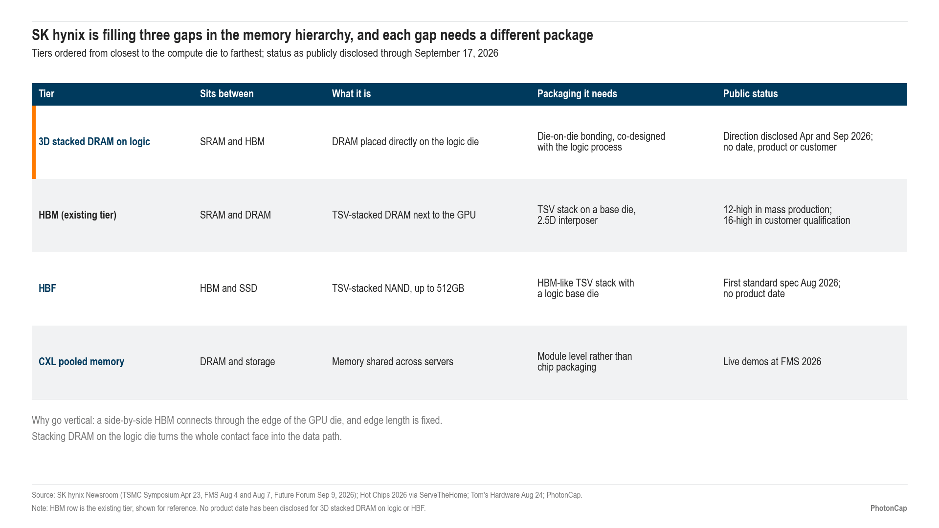
The gaps SK hynix is trying to fill in the memory hierarchy and the packaging each gap needs. Tier, product, disclosed stage and source in one table
Everything up to here is within what anyone can see in public material. Each gap needs different packaging, so packaging splits into four paths, and each path has different companies selling equipment and materials. Is there a seat that gets paid on all four paths? The slide below is the starting point.
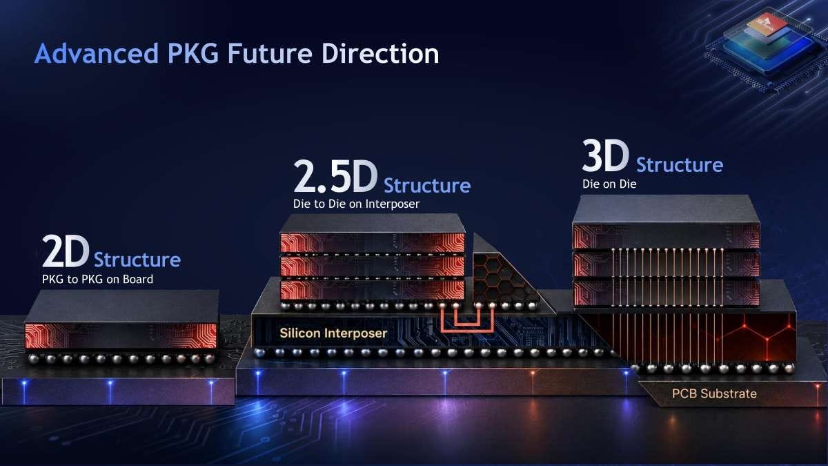
SK hynix Hot Chips 2026 slide “Advanced PKG Future Direction”. Three stages: 2D (package to package on board), 2.5D (die to die on interposer), 3D (die on die).