TL;DR
BESI grew its second quarter orders 129 percent year over year and still fell 46 percent from its June 15 all-time high to the September 14 close, and that drawdown is the price put on the signal that the adoption clock for memory hybrid bonding keeps sliding back.
One of the decisive blows was SK hynix’s remark at Hot Chips on August 23, which said that through HBM4E it stays on the existing method and hybrid bonding starts at 20-high, so on SK hynix’s schedule a window of close to three years opens as the delay window, from HBM4E mass production in 2027 to 20-high HBM5 in 2029 or later.
But what slipped is hybrid bonding on the HBM side, while logic is already shipping hybrid bonding products with Apple M5 Pro, AMD MI455X and Intel Xeon 6+, and most of the hybrid bonders BESI sells today are for logic and CPO, so the market priced in only the memory delay and the logic revenue is unchanged.
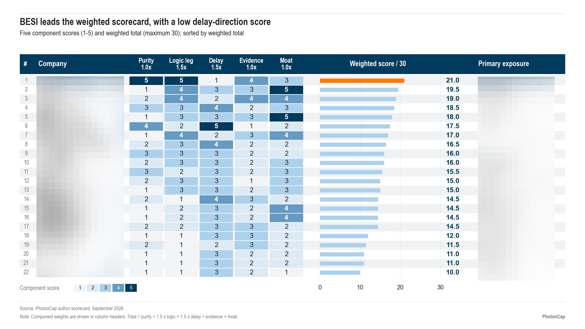
I measured, stock by stock, which direction and how far each of the 22 listed companies in the hybrid bonding value chain moved against its index on this year’s four delay shock days, March 6, July 6, July 23 and August 24, and interestingly, I think I found something. The stocks that rose on the shock days and the top stocks on this map, scored on five axes, barely overlap.
My lead is that during the three-year delay window, the money goes first to the steps before and after the bonder rather than to the bonder.
Contents
June 15 and September 10
Why I Am Drawing This Map
Background One: The 775 Micrometer Envelope
Background Two: Logic Is Already Shipping on Hybrid Bonding
What the Three Memory Makers Each Said
22 Companies and Five Layers
The Five Axes
Measured: Delay Shock Sensitivity
The Ranking, and What Happens When You Overlay Sensitivity
Company Cards
Catalyst Calendar: The Next 12 Months
Checking the Earlier Call
Closing
References & Sources
1. June 15 and September 10
BESI printed an all-time intraday high of 328.40 euros on June 15 [1], and three days later at its Investor Day it raised its 2030 revenue target range from 1.5-1.9 billion euros to 1.7-2.2 billion euros [2][3], and then it fell 46 percent from that peak in three months. The September 10 close was 184.10 euros [4], and on September 14, as I was finishing this piece, it came down once more to 175.95 euros [5].
The results numbers do not explain this drawdown. In the second quarter results on July 23, revenue was 249.9 million euros, up 69 percent year over year, and orders were 292.9 million euros, up 129 percent. Hybrid bonding customers went from fifteen at the end of last year to twenty-one [6]. Yet the stock fell more than 7 percent that day. As Morgan Stanley pointed out, the reason was reportedly that there was no hybrid bonding order from a memory customer [7]. If that happened even on a day it put out order numbers like those, then what decides this stock’s day is news about when memory hybrid bonding arrives, more than the quarterly numbers. If you have held BESI or are watching it now, you will have seen the share price shake every time that news comes up, and what I was more curious about than the size of the drawdown was what the days this stock fell hard had in common.
Of the days this year when BESI fell more than 5 percent in a single session, four were all about the same subject. On March 6, the day TrendForce relayed a Korean report that JEDEC members were discussing raising the HBM package thickness from 775 to 825 or 900 micrometers, the stock fell 17 percent on a closing basis [8][4]. On July 6, the day ZDNet Korea wrote that 16-high HBM discussions were not active and that HBM4E would also be mainly 12-high, it fell 7 percent and change [9][4]. July 23 was results day, and the three days from August 24 were the Hot Chips digestion period. In this article I will call these four days the delay shock days. Section 8 attaches the moves of the twenty-two stocks on these four days. On those four days, how many of the twenty-two stocks went the opposite direction from BESI?
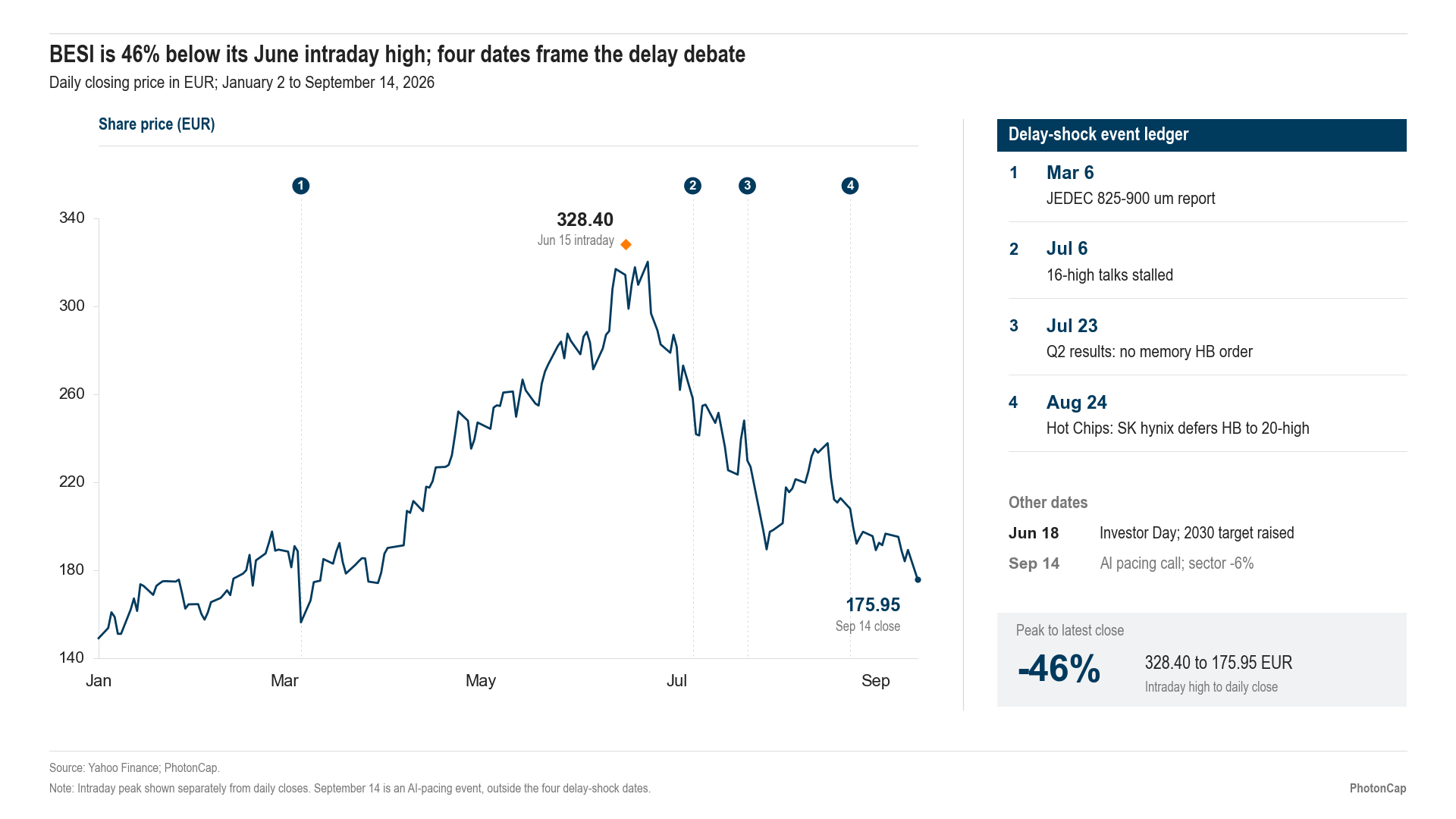
BESI daily close in 2026 with the four delay shock days and event ledger. June 15 intraday high 328.40, September 14 close 175.95
One thing needs correcting here. The market says a lot that “JEDEC relaxed the thickness spec, so hybrid bonding got pushed out,” but the only thing that is actually fixed is HBM4’s 775 micrometers. A value raised from 720 to 775 by member consensus in early 2024 was carried into the HBM4 standard (JESD270-4) published last April [10][11]. 825, 900 and 1,000 micrometers are all numbers that Korean media reported as “under discussion” in March, April and July this year, and the finalization is said to come in the second half of next year [12]. JEDEC decided nothing new in August or September.
So what happened at the end of August? A customer spoke, rather than a standard. At Hot Chips 2026, Jaesik Lee, vice president at SK hynix America, said the company goes with advanced MR-MUF through HBM4E and is preparing hybrid bonding for 20-high and above [13]. 12-high HBM4 is in mass production and 16-high is in customer qualification [14][15]. Three days later KBC Securities cut its 2030 estimates in a note titled, in effect, “the memory industry is not warm on hybrid bonding yet.” The gist of that note was that Micron has no roadmap at all, Samsung is solving bandwidth through the base die, and Nvidia is speccing toward lower stack heights [16]. If the spec discussion showed the direction, the customer’s remark nailed down the timing.
The September 14 decline was different in nature. On Saturday the 12th, Anthropic’s Dario Amodei posted that the pace of capability gains in frontier models should be slowed, OpenAI’s Altman and xAI’s Musk agreed, and Altman said an IPO this year would be too much [5]. On Monday the Philadelphia Semiconductor Index fell 6 percent, SK hynix 7 percent, Samsung Electronics, Micron and Applied 5 to 6 percent, and BESI 7 percent. That was an AI investment sentiment shock unrelated to hybrid bonding, and I did not include it in this article’s four shock days. Still, that day shows well that BESI is not a stock that moves on this one subject alone.
2. Why I Am Drawing This Map
I held BESI from February and recently sold all of it. I made a profit. But after selling, watching this drawdown, I felt I needed to look at hybrid bonding more systematically.
Companies like BESI and ASMPT do not only bond HBM. There are countless places that need bonding, like silicon photonics and optical interposers. So I think one should not judge hastily on a single event.
In May I covered seven bonding equipment companies in 7 Bonding Equipment Companies Behind HBM4 and CPO: AI’s Real Bottleneck Lives in Assembly. In that piece I set the JEDEC HBM4E thickness relaxation as the downside scenario and wrote that if the relaxation became real, MR-MUF and TC-NCF would be extended one more generation and hybrid bonding would be pushed past HBM4E. That scenario became real through customer remarks first, without the spec being finalized. Section 12 checks the items I set out then, one by one.
There are two reasons I am drawing the map again. One is that the delay window is not short. On SK hynix’s terms, HBM4E mass production is talked about for 2027, and 20-high HBM5 is talked about for 2029 and later [17][18]. The question is where the money that was riding on hybrid bonding goes during a window of close to three years. The other is that the number of challengers grew in the meantime. ASMPT is sampling a second generation hybrid bonder, Hanwha Semitech’s tool went into SK hynix for evaluation, Semes’s tool went into Samsung, and China’s Naura unveiled a D2W bonder in March. On the front end side, Applied sells an integrated line bundled with BESI, and TEL, SUSS and EV Group hold the wafer-to-wafer side.
The questions are these. Whether the hybrid bonding clock slipping a generation is confirmed, and whether that delay is already in BESI’s 46 percent. Then, where the money goes during the delay window. I answer by splitting 22 companies into five layers.
3. Background One: The 775 Micrometer Envelope
HBM is made by stacking several DRAM dies. The numbers 8-high, 12-high and 16-high are that die count. But there is a ceiling on the stacked height. It is a component that sits side by side with the GPU, so its height has to match the GPU die, and the JEDEC standard sets that height. HBM3E was 720 micrometers, and HBM4 raised it to 775 [10]. Whether 12-high or 16-high, it has to fit inside this envelope.
To fit more dies into the same envelope, each die has to get thinner. By SK hynix’s explanation, at 16-high the core dies are ground to around 50 micrometers and the gap between dies is cut to half of 12-high [13]. The number 775 itself is a ceiling that came from logic wafers being 775 micrometers thick. But the way the dies are joined to each other becomes the problem. Today’s HBM places small solder bumps between the dies and presses them together with heat and pressure. This is called TC bonding, and SK hynix uses MR-MUF, which fills liquid molding material over it, while Samsung uses TC-NCF, which inserts a film. The two methods differ in how heat escapes. In MR-MUF the liquid molding material fills the space between dies and pulls heat out sideways as well, while in TC-NCF the film stays between the dies. That is why SK hynix compared the thermal paths of the two methods side by side in its Hot Chips slides, and it used that as the argument that its own method holds up to 16-high [13]. Because there are bumps, each layer gets thicker by the bump height, and because the bump pitch is around 30 micrometers, the number of signal lines is limited too.
Hybrid bonding removes the bumps. Copper pad meets copper pad directly, the dielectric films between them are bonded at room temperature, and then the stack is heated above 200 degrees so the copper bonds to copper. With no bumps the layer gets thinner, the pitch can shrink below 18 micrometers, and because copper touches copper directly, heat escapes well. Those are the numbers SK hynix cited at Hot Chips. With hybrid bonding at 20-high, the core die can be kept 24 percent thicker than with MR-MUF, and thermal resistance, read off the slide graph, is about 35 percent lower than TC-NCF and around 25 percent lower than its own MR-MUF [13]. Two days later the company newsroom’s tech note wrote that microbump pitch is around 20 micrometers while copper direct bonding goes below 1 micrometer, and that full adoption is most likely at HBM4E or HBM5 where stacks exceed 20 layers [19].
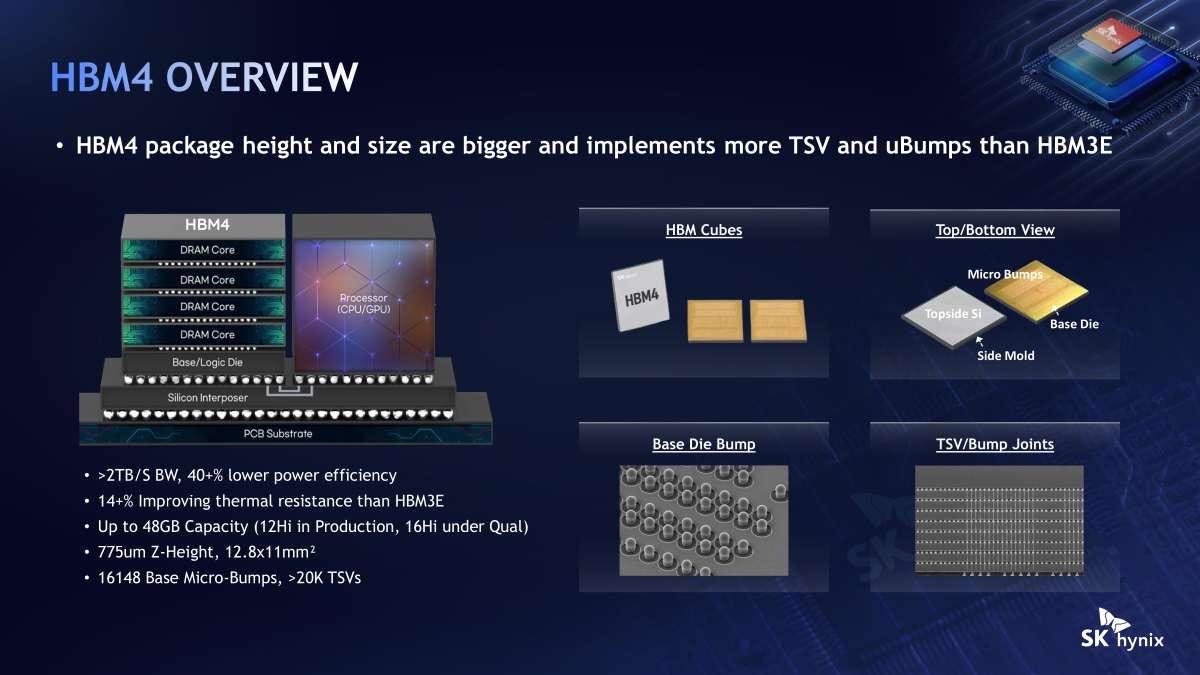
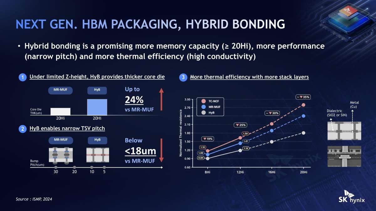
SK hynix Hot Chips 2026 presentation slides, 16-high customer qualification and the 20-high hybrid bonding plan
So why not use it at 16-high, and start at 20-high instead? SK hynix’s judgment is that 16-high fits under 775 micrometers with the existing method if the die and the gap are roughly halved. Grinding dies thinner and making bumps smaller is cheaper and more certain on yield than standing up an entirely new process. BESI itself said on the second quarter call that the hurdles on the memory side are cost and yield [20]. At 20-high that arithmetic breaks. Grind the dies thinner and they warp and crack, and the bump pitch cannot shrink further. That is why JEDEC members are discussing growing the envelope itself to 825, 900 or 1,000 micrometers, and if the envelope grows, 20-high can also go on bumps, so hybrid bonding gets pushed out one more generation. This is where the thickness discussion connects directly to bonder company share prices.
The story of stacking HBM higher is, in the end, one branch of the contest over where to add AI memory capacity. The bigger picture of whether to put it beside the GPU, stack it above, or place it far away over optics was covered in August in Beside, Above, or Beyond: The AI Memory Capacity Race and Where Optics Fits. This article looks only at one process in the “stack it above” branch, the one that joins layer to layer.
4. Background Two: Logic Is Already Shipping on Hybrid Bonding
This is the part the market tends to miss. Saying hybrid bonding got pushed out is an HBM story, and it is not a story about hybrid bonding as a whole.
TSMC’s SoIC is hybrid bonding. 3 nanometer chip stacking entered volume production in 2025, and the bond pitch shrinks from 6 micrometers in 2025 to 4.5 micrometers in 2029 [21][22]. The M5 Pro that Apple released this March is the first consumer product that joins a CPU die and a GPU die with SoIC [23], and the MI455X that AMD announced in July stacks eight 2 nanometer compute dies on 3 nanometer dies with hybrid bonding [24]. Intel attached twelve 18A tiles with 9 micrometer pitch Foveros Direct in the Xeon 6+ Clearwater Forest it launched in June [25][26]. Only Nvidia is not there yet. Rubin goes on bumps on CoWoS-L, and reports say SoIC starts with Feynman in 2028 [27].
Hyperscaler ASICs come in too. Broadcom said it started shipping the 2 nanometer 3.5D XDSiP compute SoC for Fujitsu’s MONAKA in February, and it is extending the same face-to-face hybrid bonding platform to other AI XPU customers [28]. The release of MONAKA itself is in 2027.
This is where BESI’s revenue comes from. As of the end of last year, cumulative orders for hybrid bonding systems passed 150 units, and the company said six integrated production lines built with Applied, with 30 BESI bonders, were installed at one “leading logic customer” [29]. The Investor Day material states the customer mix is “skewed to logic currently” [2]. The same material lists AMD, Intel and Apple as logic customers in production, and Broadcom ASIC and Nvidia Feynman on the roadmap [3]. So the hybrid bonders BESI sells today are mostly for logic and CPO, and memory is at the level of a few evaluation tools. The late August plunge was a reaction to news that something not yet in revenue would be later still.
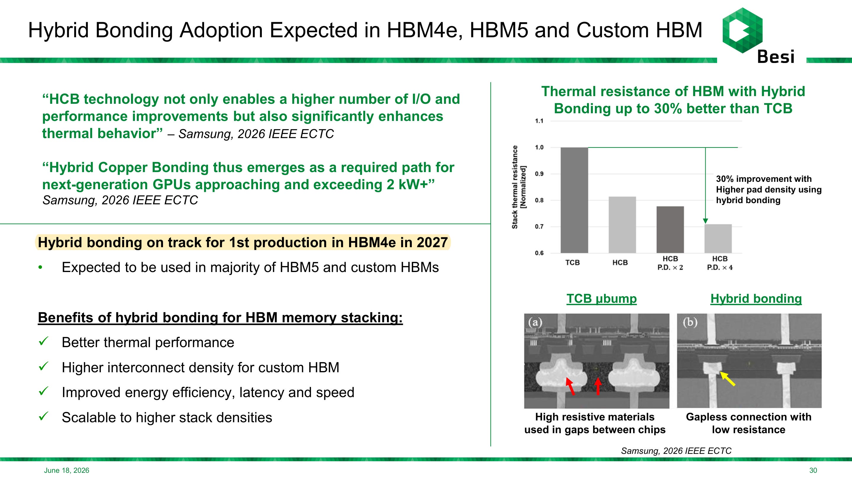
BESI 2026 Investor Day slide on hybrid bonding customer mix and 2030 targets. Source: Besi, 2026-06-18
CPO is also logic side hybrid bonding. TSMC COUPE is a structure that joins the electrical chip and the optical chip with hybrid bonding, and the April OFC piece OFC 2026 Part 3 of 5: Packaging: Glass Substrates to 3D Hybrid Bonding covered why that structure beats bumps. BESI placed CPO as one of three axes alongside logic and memory at its Investor Day [2]. The same material states that COUPE-type electro-optical chip hybrid bonding is already at the production stage, so BESI’s hybrid bonder demand is already running on two tracks, GPU stacking and CPO.
That was long, so to sum up a bit: hybrid bonding’s 2026 revenue is logic, and the timing of volume adoption in memory, which was the growth story for 2027 onward, has been pushed back. SK hynix points to HBM5 and later, and only Samsung leaves open the possibility of earlier adoption at HBM4E. The market priced only the second, and the first is intact.
5. What the Three Memory Makers Each Said
But the three memory makers did not say the same thing. This is where the second axis of this map splits, so I write it in a little detail.
SK hynix is the clearest. MR-MUF through HBM4E, hybrid bonding from 20-high [13]. Research continues, though. In February it reportedly ordered one Kinex inline tool, the Applied and BESI bundle, for a development line at somewhere between 15 and 20 billion won [30], and in April Hanwha Semitech’s second generation hybrid bonder reportedly went in as an evaluation cluster [31]. Internal verification of 12-high hybrid bonded HBM was declared complete by the responsible team lead at an April conference, with the caveat that yield is better than two years ago but the economics are not there yet [32]. To sum up, the picture is buying the tools but mass producing from HBM5.
Samsung Electronics was, by contrast, the side pushing ahead. It sent hybrid bonded HBM4 samples to Nvidia, and in the May ECTC paper HCB lowered the thermal resistance of the HBM stack itself by about 19 percent versus TCB, with the improvement growing to 22 to 29 percent under higher pad density [33][34]. According to a July report by The Elec, it decided to build a mass production line of about 50 D2W hybrid bonders at Pyeongtaek P5 and put BESI at the top of the list, but at about 6 billion won per tool, double the competitors, negotiations over structural changes and price are reportedly dragging on [35]. Move-in from the end of this year, and the internal target for large-scale mass production is 2030. What Samsung emphasized at Hot Chips was the base die and side cooling rather than hybrid bonding [14]. Samsung’s official statement on hybrid bonding is actually on the January fourth quarter results call. It applied HCB to HBM4, delivered samples to major customers in the prior quarter, and plans partial commercialization at the HBM4E stage. On the same call it also said customer demand for 16-high HBM4 is very limited, so mass production is unnecessary [36]. At SEMICON Taiwan on September 1, it laid out a roadmap of HBM5 in 12-high, 16-high and 20-high with mass production around 2028, and zHBM from 2029 onward [37]. If 20-high HBM5 is 2028, that matches the timing of the P5 line. The Samsung packaging roadmap seen in July in TSMC Is Ahead in CPO. Samsung Is Putting a Third Chip Next to HBM sits on that extension.
Micron did not show a hybrid bonding roadmap at Hot Chips. It went as far as saying there is a good path to 16-high and a lot of work remains beyond that, and its slide merely listed liquid cooling, hybrid bonding, and solder and side mold changes side by side as candidate answers to the thermal problem [38]. It said in its results release that HBM4E goes to a TSMC base die in 2027 [39].
One more variable attaches on the buyer side. In early August TrendForce wrote that Nvidia had begun widening its evaluation of the HBM configuration for the 2027 Rubin Ultra, from the original 12-high HBM4E to 8-high HBM4E and HBM4 [40]. The reason given was that next year’s HBM bit supply cannot keep up with demand. If the largest customer moves toward lower stacks, the point at which 16-high is needed itself moves back, and then the point at which hybrid bonding is needed moves back further. That report was three weeks before Hot Chips. On September 9, KLA also said at the Citi conference that some HBM customers are moving from 12-high to 8-high configurations because of memory price pressure [41]. The same story, from an equipment maker’s mouth.
Put the three companies on one line and it reads: SK hynix deferring, Samsung negotiating, Micron silent. The sentence BESI wrote at its Investor Day, “first memory production in 2027, starting with 16-high HBM4E,” [3] does not match these three lines. The only company that could keep that sentence in 2027 is Samsung, and Samsung is cutting the price right now.
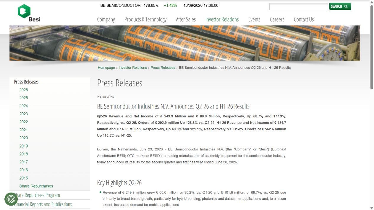
Top of BESI’s Q2 results release, orders of 292.9 million euros and 21 hybrid bonding customers. Source: Besi, 2026-07-23
The 292.9 million euros in orders and the twenty-one customers in the capture above are as far as the picture goes from public sources, and the market saw those numbers and still pulled the stock down more than 7 percent that day. So the next question is how the other companies bundled under the same theme as this one took the same delay news, and from here on it is a picture you only see by overlaying public sources on each other. In the paid section I place the 22 companies in five layers around the bonder, score them on five axes, and on top of that attach, stock by stock, how far each one actually moved against its local index on the four delay shock days. The scores are my judgment, so I measured separately how the market actually saw it and overlaid that, and one axis is the signature of this map, measuring company by company whether a hybrid bonding delay is a gain or a loss. So the question becomes this. Whether the stocks that rose on the days the bonder fell are sitting in a position that keeps gaining through the three-year delay window. To give you one line in advance, the number one on this map is the stock that fell 46 percent, and number two is a company that sells no bonders at all.