
[OFC 2026] Part 3 of 5: Packaging: Glass Substrates to 3D Hybrid Bonding
Corning, UC Davis, and Sumitomo

Introduction
The AI infrastructure race has moved beyond chip design into packaging.
No matter how fast GPU and switch ASIC performance scales, the optical interconnect that moves data off-chip becomes the bottleneck if packaging cannot keep pace. Co-Packaged Optics (CPO) attacks this bottleneck head-on by pulling the optical engine inside the switch package, minimizing electrical interconnect length, and improving both bandwidth and power efficiency simultaneously.
The question is “on what substrate, and how do you attach the chips?” The answer to this question determines the path to CPO commercialization.
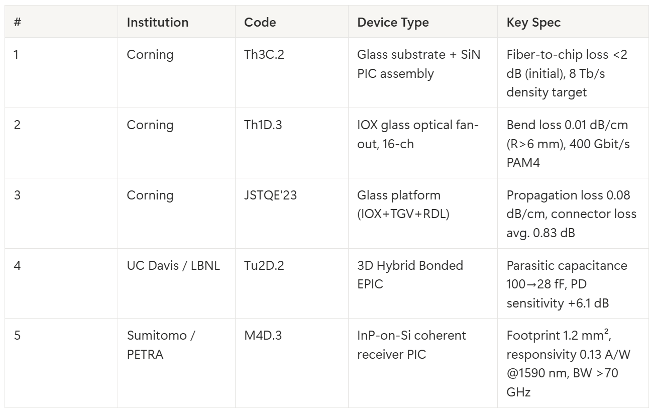
This installment analyzes technologies that answer this question in different ways, drawing on four papers presented at OFC 2026 and one foundational journal paper. Corning demonstrated its “glass platform” through two OFC papers, with a 2023 JSTQE paper providing the underlying technology base. UC Davis / Lawrence Berkeley National Lab presented the world’s first 3D hybrid-bonded EPIC demonstration with solder completely eliminated. Sumitomo / PETRA introduced a compact InP-on-Si PIC that resolves the L-band coherent receiver trade-off through heterogeneous integration.
All five papers share a single core message: packaging technology determines system performance.
Five Papers at a Glance
CPO Packaging Technology Comparison
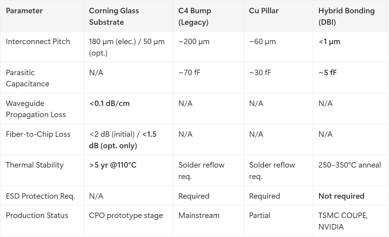
From here, I analyze each paper individually, examining where each technology sits in the CPO packaging stack, its limitations, and structural insights across the full value chain.
