
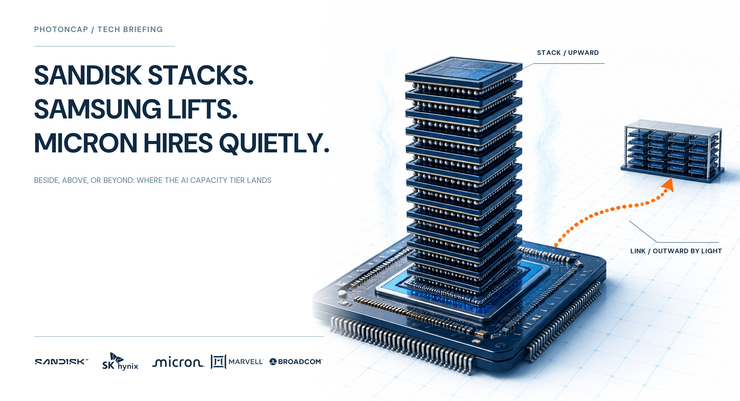
On August 13, one slide was shared at the Sandisk Investor Day. The content was that Meta joined the HBF consortium following Google, and ten days earlier, the first HBF standard specification of up to 512GB and up to 3.0TB/s was published through OCP. Ironically, in the same week, Samsung brought out the zHBM concept that stacks memory vertically on top of the accelerator. Then the question, naturally, has a place it heads to. What about Micron? Micron is officially not putting its name in this game. However, the phrase “stacking NAND” points to a completely different structure at each company, and if you do not distinguish them, you end up drawing the beneficiary map wrong. So this article is going to try dividing the question into two. How to stack, and where to place the capacity made that way, relative to the processor. My interpretation is on the side of “whichever direction the stacking competition gets settled, wouldn’t a considerable part of the growth go not to the memory companies but to the optical interconnect layer?” The evidence has been prepared with job posting originals and physics arithmetic.
Contents
August 13, One Slide at Investor Day
Three Meanings of the Word “Stacking”
Micron’s Public Stance and the Careers Site
The Structure Micron’s Job Postings Draw
Beside, Above, Beyond: Three Paths and Three Walls
Microseconds and Meters: The Physical Reason NAND Is Allowed to Move Away
The Optics Map: Which Layer It Falls On
Stacking Equipment and Optical Links: The Related Names
Conclusion
1. August 13, One Slide at Investor Day
Let me start with the $SNDK story. Sandisk stock rose 6% on August 12 alone and reached the mid $1,300 range (as of the 2026-08-12 close) [3], and on the 13th, the day of the Investor Day, it rose another 14% and closed at $1,528 (as of the 2026-08-13 close) [1][4]. In terms of the gain since the start of the year, it is over five times, remarkably [3][4]. It is true that the NAND shortage cycle made these numbers, but the place where my eyes stayed long that day was one slide on the technology roadmap side, rather than the financial targets page.
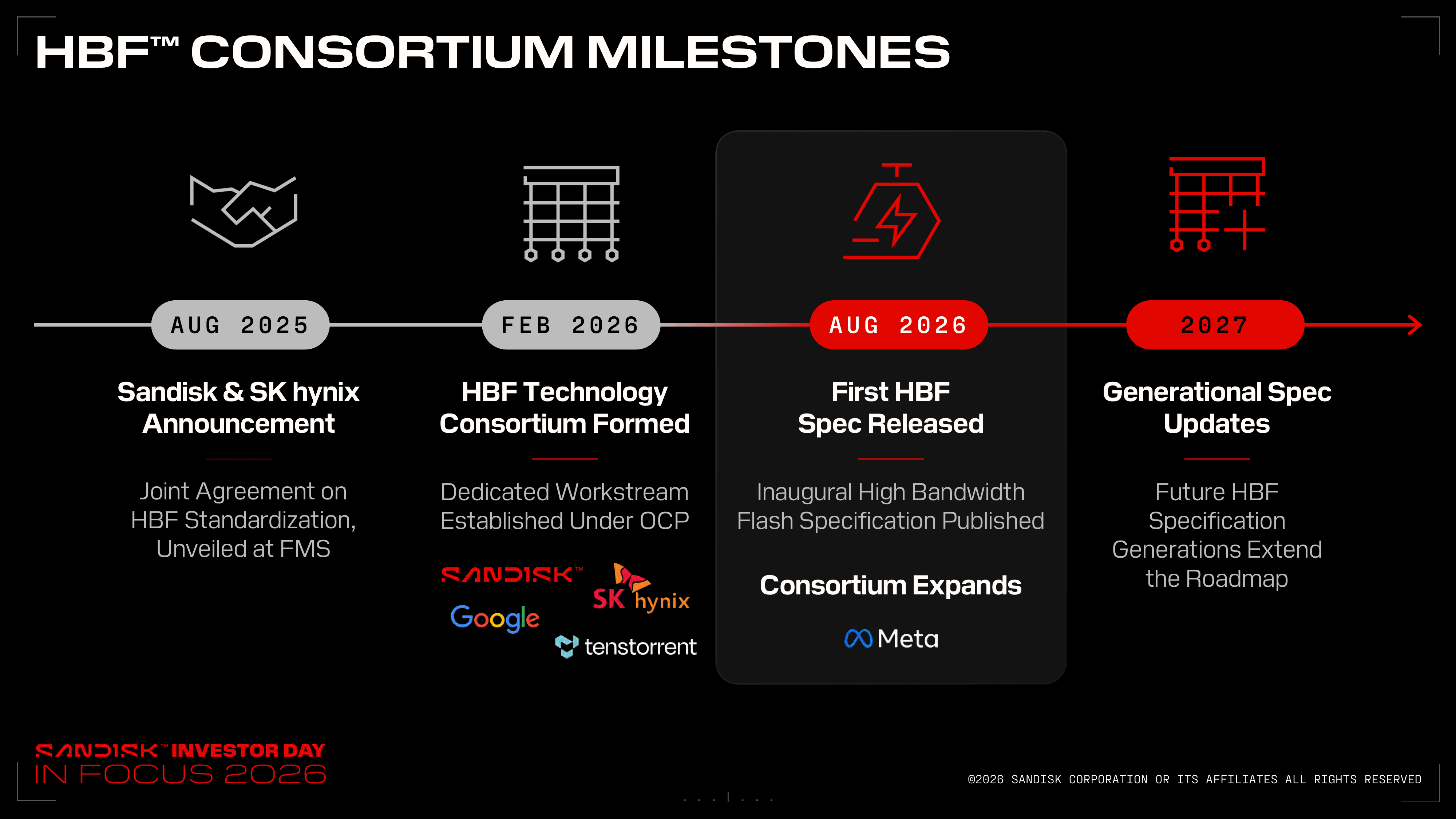
The “HBF Consortium Milestones” slide from the Sandisk 2026 Investor Day. The August 2026 milestone shows “Consortium Expands: Meta”
The timeline of the slide reads like this. In August 2025, Sandisk and SK hynix agreed on HBF (High Bandwidth Flash) standardization, and in February 2026, a consortium was formed under OCP (Open Compute Project, the body where hyperscalers turn hardware specifications into open standards). The ones that joined at that time were Google and Tenstorrent [5][7]. Until then there did not seem to be much reaction, but just recently, in August 2026, when the first standard spec was published and the Meta logo went up in the consortium expansion box [1], the mood really became one of wondering whether HBF is going to become the standard. In other words, to organize it again, two hyperscalers that design their own AI chips, namely Google and Meta, are now in a state of having put their names on a NAND-based memory standard.
What HBF is, I covered in January in HBF (High Bandwidth Flash) and Optics: The Missing Link in AI Infrastructure, and at that time, it was the article with the best response among the ones I had posted on my Substack.
To say it again in one line, it is a plan to transplant HBM’s stacking formula onto NAND and create a middle tier that is “much wider than SSD and much bigger than HBM.” At that time it was at the level of conference presentations and concepts. Now, a concrete spec document with 512GB capacity, three bandwidth grades from 0.4 to 3.0TB/s, and a UCIe interface is up on OCP [5][6], and it has come to the stage where the company states a schedule: samples in the second half of this year, inference devices in early 2027 [5]. At the Investor Day they went one step further, and it is said that the tape-out of the first HBF die (the state of having finished the design and handed it to the foundry) is complete and customer samples are next year [4].
So the material the market encountered this week is two things. On the surface there are the NAND price cycle, the contract backlog that has grown to the $90 billion range [4], and the Investor Day’s long-term financial targets [2], and below that there is the structural change that “NAND comes out of the storage box and climbs onto the memory bus.” This article intends to deal with the latter. And the question is one.
Everyone says they are stacking NAND, but are they stacking the same thing?
2. Three Meanings of the Word “Stacking”
Before the main body, it would be good to divide the axes first. The news of “stacking NAND” actually has two different questions mixed in it. One is the process question of how to stack and build, and the other is the placement question of where to put the capacity block made that way, relative to the processor. This section is the former question, and the beside, above, and beyond in the title are the latter question.
Starting from the process side, the word “stacking” in the industry right now points to three different processes. The three differ in purpose, and the direction the money flows is also different.
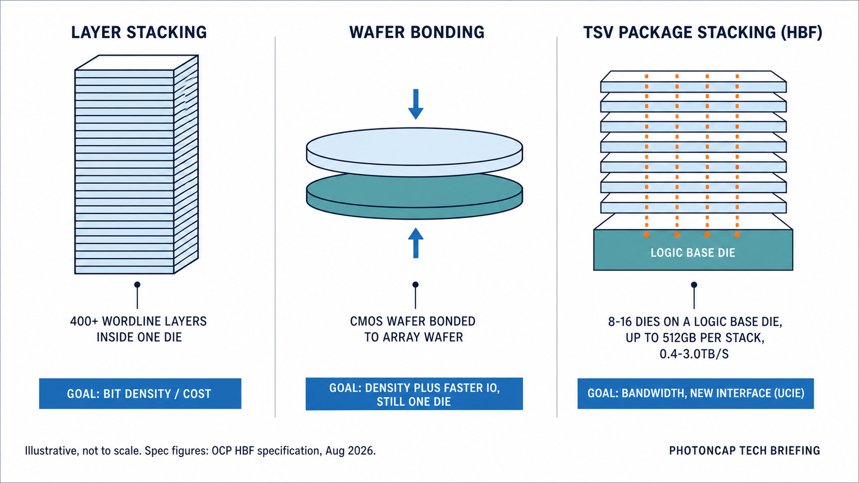
Concept diagram of the three kinds of stacking. Layer stacking, wafer bonding, and package-level TSV stacking compared in one view
The first is layer stacking. It stacks NAND cells vertically inside the die, and the “hundreds-of-layers NAND” we see in the news is all this story. It is said that Samsung V10 has passed 400 layers, Kioxia and Sandisk’s BiCS10 is 332 layers, and Micron G9 is 276 layers [8][9][10]. The purpose is simple. Extracting more bits from the same wafer and lowering the cost. It is the economics of storage devices, and it is a game that every NAND company is playing without exception.
The second is wafer bonding. It is a method of making the NAND cell array wafer and the peripheral circuit (CMOS) wafer separately, then attaching them whole to complete one die. Kioxia and Sandisk went first under the name CBA [9], and Samsung also announced that it is joining this column from V10 under the name BV-NAND [8]. Up to here, it is still a story about “how to make one die well.” Density increases and I/O gets faster, but the completed die still sits behind the SSD controller, behind the serial passage called PCIe.
The third is HBF. It is a structure that threads multiple completed NAND dies with TSV (Through-Silicon Via, vertical wiring that penetrates the die) like HBM, puts them on a logic base die, and connects them directly with a wide parallel bus from the seat beside the processor [5][6]. The first spec is 8-high or 16-high stacking, up to 512GB per stack, and bandwidth from 0.4 to 3.0TB/s depending on grade [6]. If the previous two stackings are the game of “cheaper,” this one is the game of “wider.” Since it is a matter of changing the interface itself from the storage kind (serial PCIe) to the memory kind (parallel wide bus), I see only this third one as a stacking of a different nature.
But here, one placement question cuts in ahead of time. It is the option of moving the stacking position onto the processor entirely. The zHBM that Samsung unveiled at FMS 2026 is a concept that stacks not NAND flash memory but HBM vertically right on top of the accelerator, and by the company’s claims, it speaks of 8 times the performance of HBM5 and more than 10 times the density [8]. Let me clearly attach the maturity label that it is still at the concept model stage. It is not a product, not a confirmed roadmap, and the figures are vendor claims. Still, the direction itself needs a serious look, because as covered in July in TSMC Is Ahead in CPO. Samsung Is Putting a Third Chip Next to HBM, Samsung keeps digging into the real estate problem inside the package from different angles. And that makes sense, because Samsung is a vertically integrated semiconductor company that can optimize the processor, memory, HBM, photonics, and process together, so it may well be making various attempts. I also think this point is their strength.
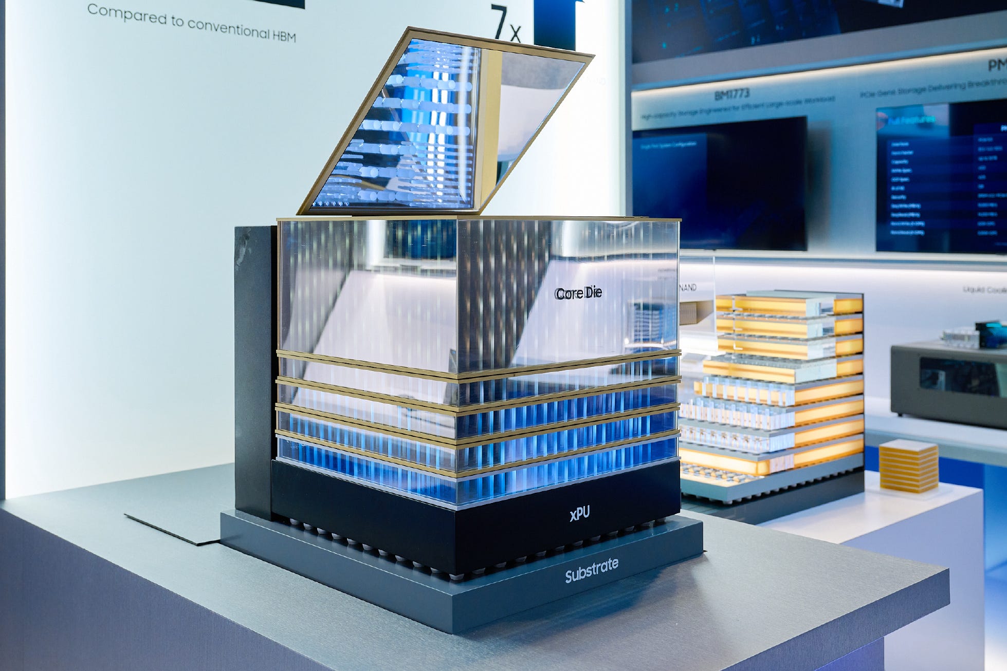
Concept diagram of the zHBM structure from the Samsung newsroom. A cross-section with the HBM stack placed on top of the processor
That was long, so to organize it a little: the layer-count competition and the bonding transition are the stacking of cost, HBF is the stacking of bandwidth, and zHBM is the stacking of position. The reason investors must not lump the three into one word is, as we will see later, that the physical limits each one hits are different.
3. Micron’s Public Stance and the Careers Site
Now it is Micron’s turn. In fact, Micron is not a member of the HBF consortium [7]. The award it received at FMS 2026 is also said to have been on the 245TB-class data center SSD side [11]. In early August at the Technology Leadership Forum, the remarks of CBO Sumit Sadana also stop at the level of “when DRAM is insufficient, KV cache spills over to the NAND side” [12].
To summarize, the Micron on public stages concentrates its firepower on HBM4 and sells NAND as fast SSDs. It stacks, but in the first and second meanings of stacking, that is, the stacking of cost.
Then is Micron really keeping its hands off the third game?
Actually, in January this year I made an inquiry to an acquaintance, and since it seemed difficult to talk in a public place about the answer I heard privately, only now have I found public materials and come to make it public.
If you open the careers site, the answer comes out somewhat different.
This part took some time to confirm. Nothing came up in news searches, so I went through Micron’s recruiting system directly, keyword by keyword, and the word “HBF” is 0 cases in all postings. Instead, two postings from the NAND design organization (NVEG) in Tokyo were caught. One was posted in April, one in July, a hiring that has continued for four months [13][14], and since postings can come down, I saved the originals as captures.
Please look at the highlighted phrase in the capture below. What structure of NAND this posting is hiring for, and why I crossed over to the optics-side conclusion after seeing it, is the content of the paid section.
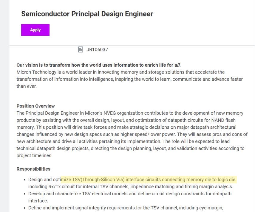
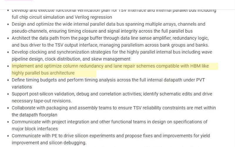
Original Micron Tokyo NVEG job posting.
