
HBF (High Bandwidth Flash) and Optics: The Missing Link in AI Infrastructure

If HBM (High Bandwidth Memory) was essential for the AI training phase, HBF (High Bandwidth Flash) is now being discussed as a new alternative with the full-scale opening of the inference market.
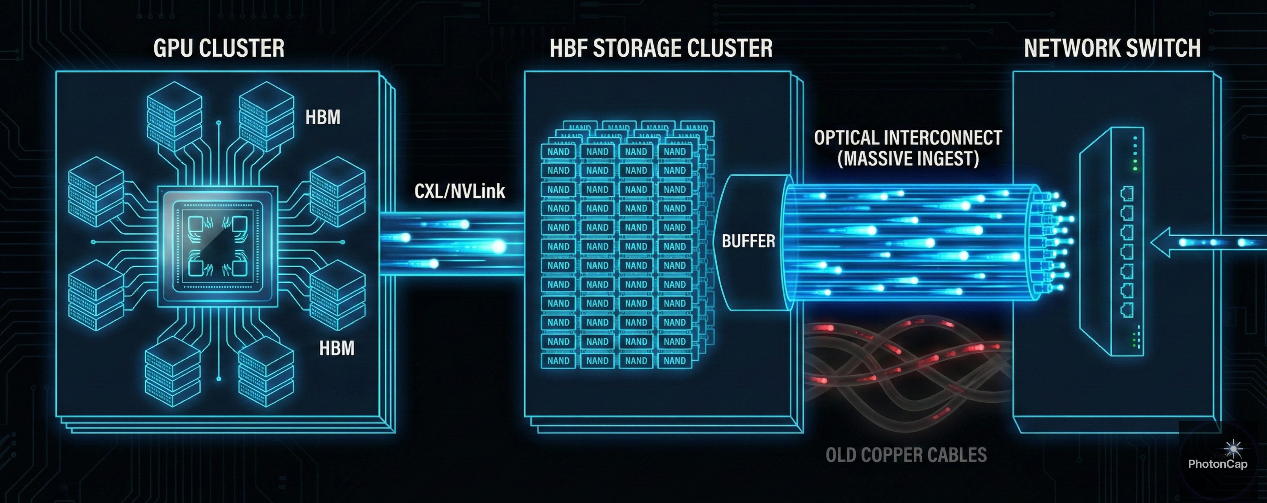
Before diving into the technical analysis, let’s first examine the architecture comparison chart presented by Professor Kim Jung-ho of KAIST. This diagram clearly illustrates why current AI systems have reached their limits and how HBF aims to turn the tables.
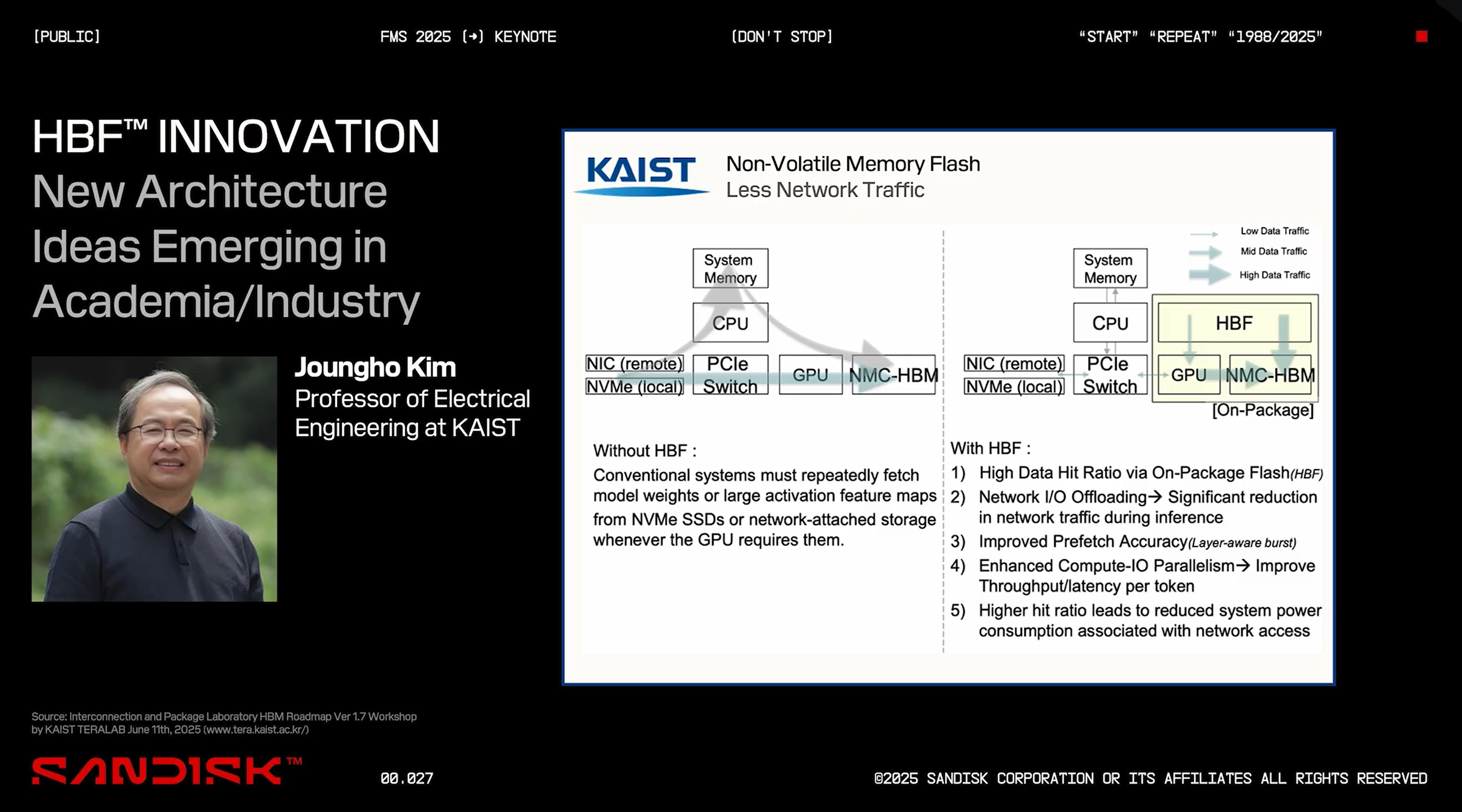
Left (Without HBF): Existing systems required the GPU to fetch massive model weights or data from remote NVMe SSDs or network storage every time it performed inference. This process involved traversing PCIe switches, causing severe bottlenecks and power waste.
Right (With HBF): In contrast, the HBF architecture brings large-capacity NAND directly onto the GPU package. This shifts the structure from ‘fetching data’ to ‘keeping it nearby for use,’ dramatically reducing network traffic (offloading) and maximizing the system’s energy efficiency.
Ultimately, HBF is not merely memory; it is a structural innovation aimed at reducing data movement distance to near zero.
Considering Professor Joungho Kim’s proposal alongside NVIDIA’s next-generation storage strategy (including ICMS), the emergence of HBF is highly likely to become a significant trigger accelerating the expansion of the optical interconnect ecosystem, going beyond a simple speed improvement for NAND. We analyze its technical background and potential beneficiary companies.
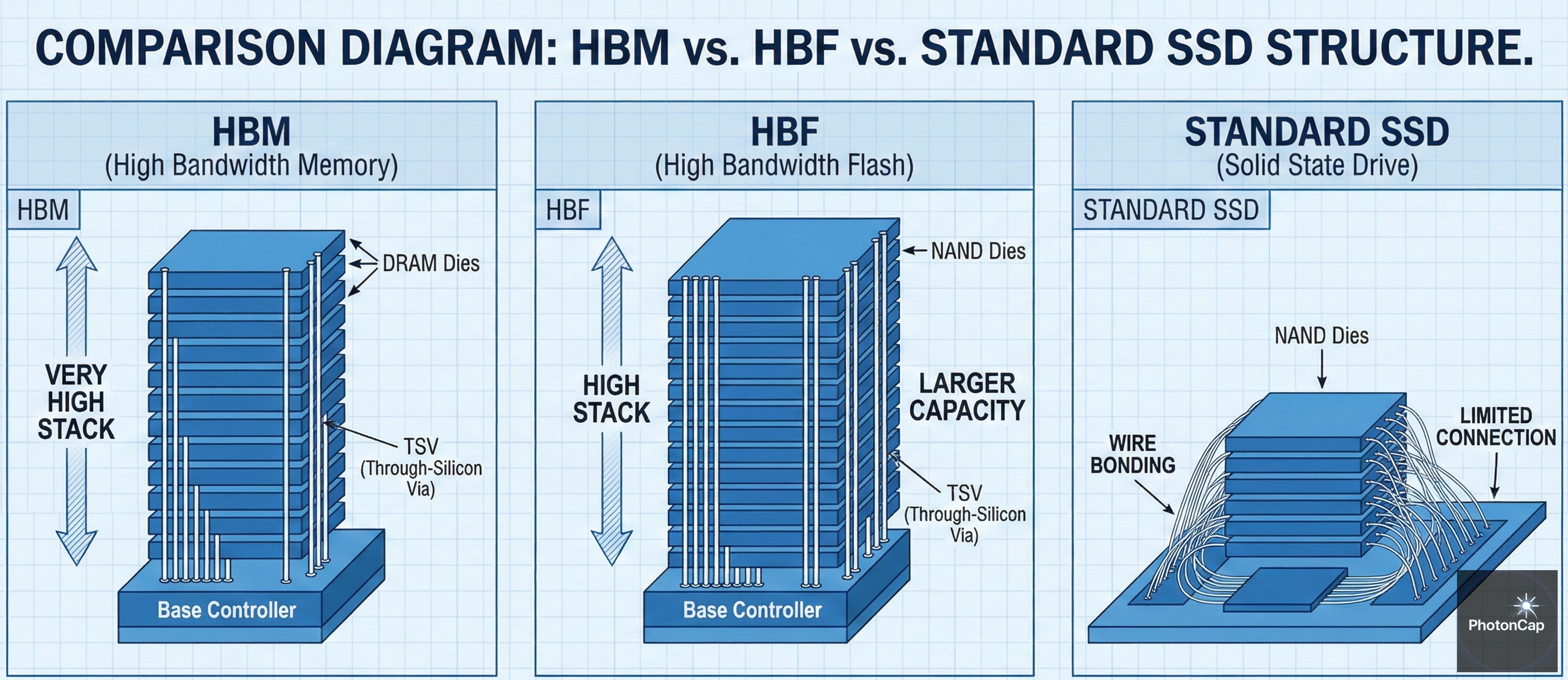
1. Technical Definition of HBF (High Bandwidth Flash)
HBF is a next-generation packaging concept aiming to apply HBM’s successful formula—3D stacking using Through-Silicon Vias (TSVs) and interposer technology—to NAND flash. Its core lies in connecting vertically stacked dies in parallel to simultaneously achieve high capacity and high bandwidth.
Structural Features: While conventional NAND packaging primarily uses wire bonding, HBF aims to implement thousands of TSVs within the NAND die itself. This dramatically shortens signal paths and enhances parallelism.
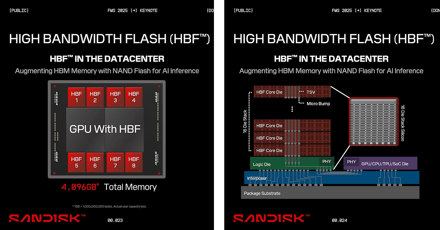
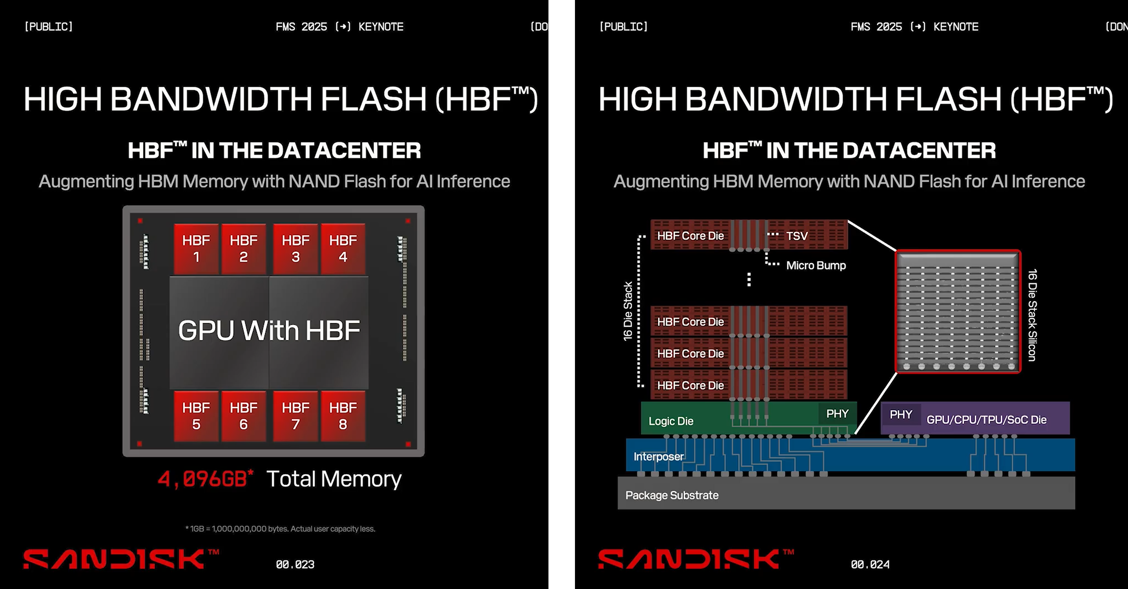
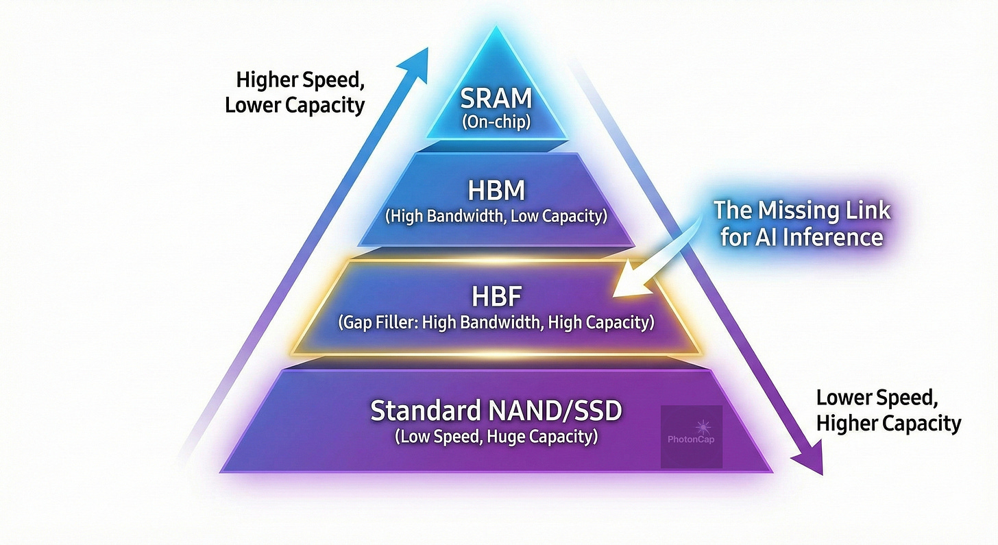
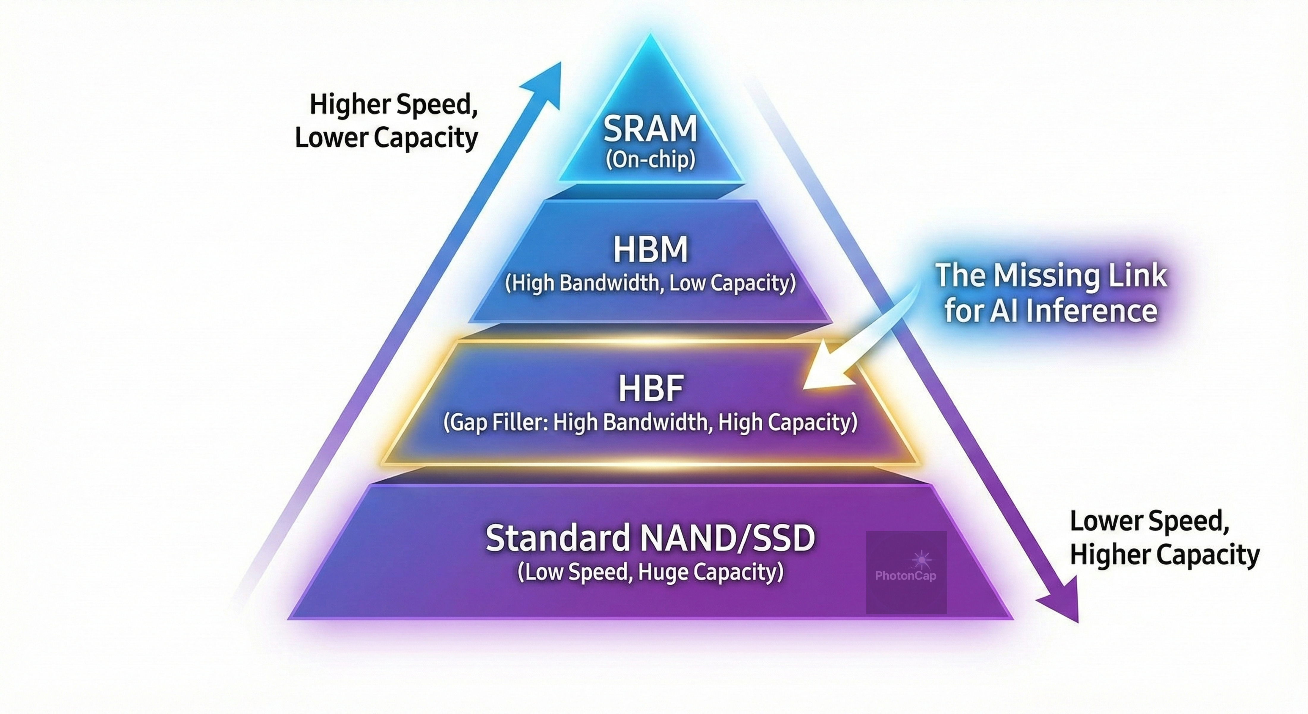
Performance Goals: The objective is to achieve tens of times greater I/O bandwidth (terabytes-per-second-level system bandwidth) compared to existing PCIe/NVMe-based SSDs, while also delivering terabyte-level capacity—a scale difficult to achieve with HBM architecture.
(Summary/Analogy: Expanding the SSD’s input/output from a two-lane highway to a 1,024-lane superhighway, creating a structure that can rapidly discharge vastly larger data volumes than HBM, albeit at a slower rate.)
2. Background: Why HBF? (The ‘Memory Wall’ in Inference)
The rise of HBF stems from two key factors: the KV Cache bottleneck encountered during LLM (Large Language Model) inference and NVIDIA’s shifting storage strategy.
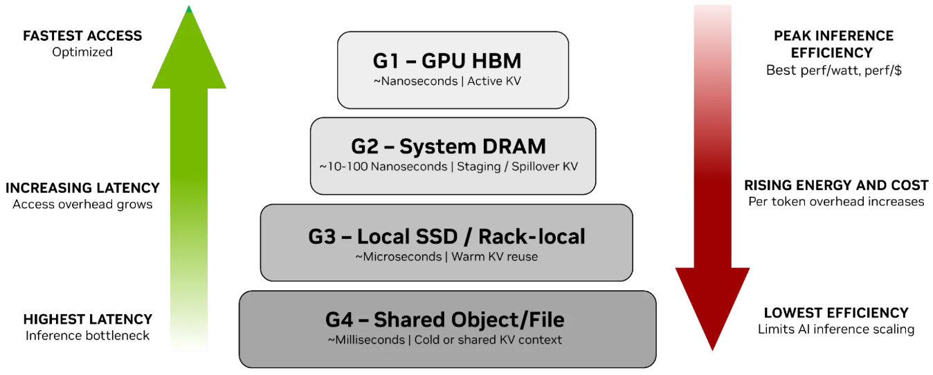
KV Cache Bottleneck: During inference processing long contexts, AI must reference previous conversation data in real-time. This data (KV Cache) is so massive that keeping it all resident on expensive HBM (DRAM) is inefficient, while loading it from standard SSDs introduces significant latency.
Performance Gap: The extreme speed difference between DRAM (ns-level) and NAND (µs-level) degrades system efficiency.
ICMS (Inference Context Memory Storage): To address this, companies like NVIDIA are exploring ‘hierarchical memory storage’ solutions that offer greater capacity than HBM and faster speeds than SSDs. HBF is one of the leading candidate technologies best positioned to meet these requirements.
3. Potential Beneficiaries of HBF Adoption (Memory Sector)
If the HBF market opens, success will hinge not on simple NAND production capacity but on ‘Advanced Packaging’ capabilities. However, HBF is currently closer to a technical concept stage than a concrete product, and should be approached as a mid-term structural change rather than an immediate performance driver.
(1) SanDisk ($SNDK): At ISSCC 2025, SanDisk and Kioxia demonstrated their unrivaled technological prowess by announcing 4.8 Gb/s ultra-high-speed I/O and PI-LTT (Power Isolated Low-Voltage Termination) technology. These form the technical foundation for Flash layers capable of evolving into HBF. They are the ‘concept designers’ group that proposed the HBF concept to academia and have led its standardization. They have identified HBF as the next-generation growth engine to overcome the universal NAND downturn and are spearheading R&D. SanDisk, in particular, is strongly pushing HBF as its independent AI memory solution following its spin-off.
(2) Kioxia ($OTCMKTS: KXIAY): A partner sharing R&D and factories with SanDisk for over 20 years, jointly developing HBF core technology.
(3) SK Hynix ($KRX: 000660): Leveraging TSV and advanced MR-MUF process technologies proven through standardization cooperation with SanDisk and dominance in the HBM market, SK Hynix is transplanting these capabilities to NAND. It is executing a visible AI-NAND (AIN) roadmap, including sampling in the second half of 2026. It announced plans to build a next-generation AI-NAND (AIN) lineup, including High Bandwidth Flash (HBF).
(4) Samsung Electronics ($KRX: 005930): It aims to widen the gap with competitors by integrating foundry (contract manufacturing) production methods into memory. It plans to apply the foundry’s advanced 14nm-class FinFET process to the NAND logic (Peripheral) section. Its ‘AI turnkey solution’ capability, spanning foundry-memory-packaging, is a powerful weapon.
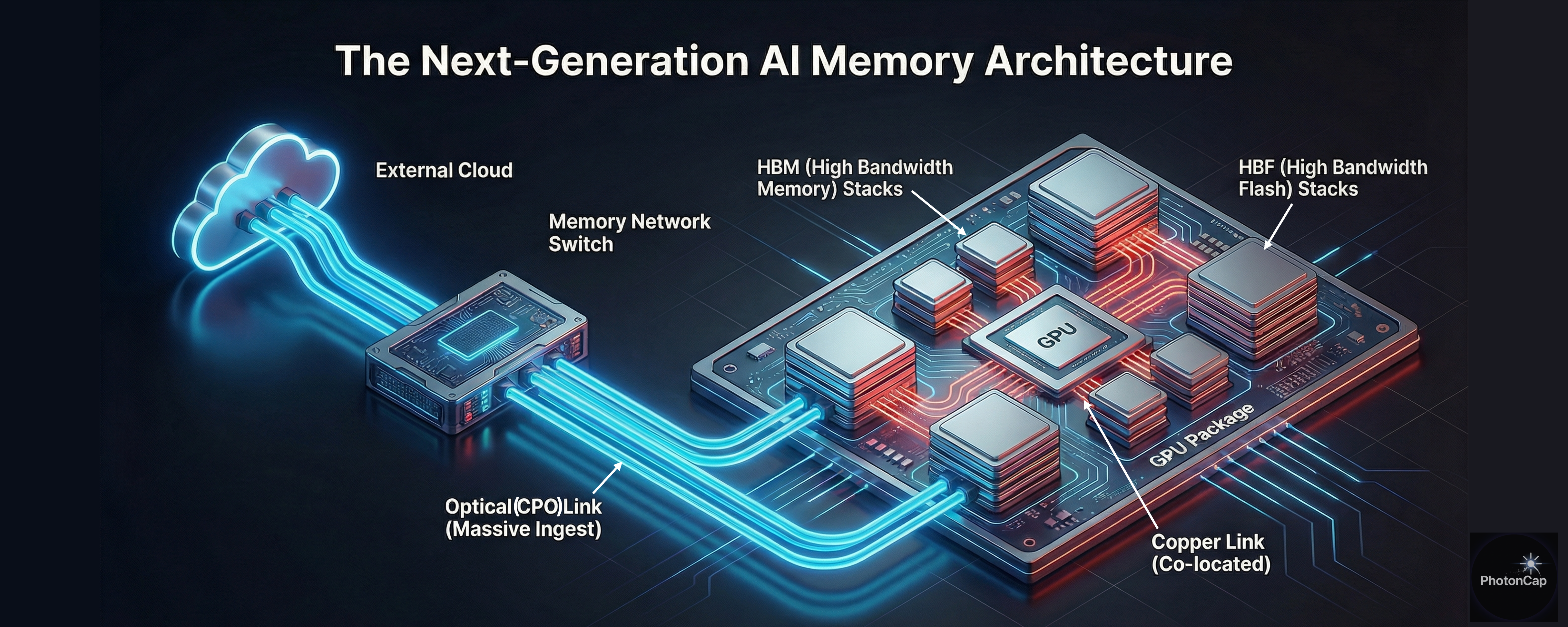
4. The Link Between HBF and Optics: Bandwidth Expansion and Transmission Limits
The adoption of HBF dramatically intensifies the phenomenon of ‘Data Gravity,’ where data becomes concentrated at specific locations with ultra-high density. With ultra-high-speed I/O opening up at 4.8 Gb/s per NAND die and several TB/s per package, the bottleneck now shifts from the ‘storage device’ to the ‘interconnect’ that transports the stored data to the processor (GPU/DPU).
(1) Physical limitations of electrical signals (Copper): Existing copper cables (PCIe, NVLink, etc.) see their transmission distance (Reach) drastically shorten as bandwidth increases. Entering the PCIe 6.0/7.0 era, the effective reach of copper cables has diminished to tens of centimeters. Signal integrity and heat dissipation issues have reached critical thresholds for transmitting the massive data volumes HBF generates across rack-level distances.
(2) The Energy Efficiency Dilemma: Energy consumption for long-distance transmission of data as electrical signals increases exponentially. With HBF causing an explosion in the volume of data (throughput) to process, clinging to existing methods leads to a paradox: massive power is wasted solely on data transmission, leaving insufficient power for the critical computation (Compute) tasks.
(3) Expanding the Role of Optics:
Rack-Scale Communication: High-capacity data movement between storage servers and GPU servers equipped with HBF.
CXL over Optics: A means to overcome distance constraints when the CXL interface is extended at the rack level for memory pooling.
(4) Outlook: As HBF expands “storage” bandwidth, the need for CPO (Co-Packaged Optics) or LPO (Linear Drive Optics) technologies will grow to match “transfer” bandwidth.
(Summary/Analogy: HBF is like fully opening a dam’s floodgates. To prevent data from flooding and ensure smooth flow, the waterway (transport network) must be expanded with wide-diameter pipes (Optics).)
5. Key Players in the Optics Ecosystem
To transmit the 4.8 Gb/s ultra-high-speed I/O and terabyte-per-second (TB/s) bandwidth provided by HBF without system loss, optical interconnect companies aiming to overcome the limitations of existing copper cables are emerging as key beneficiaries in the ecosystem.
(1) Broadcom ($AVGO)
Key Focus: An absolute leader in the optical DSP (Digital Signal Processor) and high-speed switch markets.
Key Role: Provides the ‘backbone’ of HBF infrastructure through its DSP chipsets that convert HBF’s high-speed optical signals to digital and its Tomahawk 6 (100 Tbps) switches that handle massive traffic. Its CPO (Co-Packaged Optics) technology, which places optical engines directly next to ASICs, is essential for achieving HBF’s power efficiency goals.
(2) Marvell ($MRVL)
Key Point: Recently completed the acquisition of Celestial AI for approximately $3.25 billion, evolving into an optical connectivity platform company.
Key Role: Through its core acquired technology, ‘Photonic Fabric’, it is leading the next-generation interconnect standard that optically integrates GPUs and HBF, connecting memory and computing resources within data centers like a single massive chip.
(3) POET Technologies ($POET)
Key Point: Possesses proprietary Optical Interposer technology**.**
Key Role: It is the only hybrid integration solution enabling low-cost placement of optical engines directly adjacent to the HBF stack. It specializes in minimizing copper wiring segments between chips and modules to eliminate data bottlenecks and maximize power efficiency compared to existing solutions.
(4) Ayar Labs (Private)
Key Feature: It possesses technology to embed the ‘TeraPHY’ optical I/O chiplet directly within the chip package, rather than placing the optical module externally. It is building an ecosystem alongside ‘SuperNova’, the external light source device that drives it.
Core Role: It optically initiates the data pathway from HBF to the GPU starting from within the chip itself. By replacing the existing electrical physical layer (PHY), it has the potential to reduce power consumption to one-tenth and expand bandwidth density up to 1,000 times.
(5) Lightmatter (Private)
Key Point: Owns ‘Passage’, a multidimensional interconnect platform that optically connects chips.
Core Role: It binds tens of thousands of chips into a single massive optical neural network. Instead of converting data from HBF into electrical signals for routing, it assigns paths directly in the form of light (Optical Routing), achieving near-zero data transmission latency.
(6) Xscape Photonics (Private)
Key Feature: Possesses high-density wavelength control technology that transmits dozens of wavelengths over a single optical fiber.
Core Role: It maximizes transmission efficiency by expanding the number of lanes (wavelengths) on the data highway by tens of times, alleviating bandwidth bottlenecks caused by HBF’s ‘data gravity’.
6. Expanded Ecosystem
NVIDIA ($NVDA): The architect of the HBF and ICMS ecosystems. NVIDIA’s GPUDirect Storage (GDS) technology, which feeds HBF’s massive data directly to GPUs bypassing CPUs, and the BlueField DPU’s role in managing data movement load are absolutely critical. If HBF is the hardware, NVIDIA holds the software/network power to control it.
Hanmi Semiconductor ($KRX: 042700) / ASMPT ($OTCMKTS: ASMVY): The “trickle-down effect of Advanced Packaging“ extends to NAND. Like HBM, precision stacking technology is also core to HBF. This opens the possibility for additional demand for NAND TSV bonding equipment (like TC Bonders) and Hybrid Bonding equipment, following HBM equipment.
7. PhotonCap’s Insight
HBF is not merely an evolution of storage devices. It should be interpreted as the next step in the AI infrastructure architecture, progressing through “Compute (GPU) - Memory (HBM) - Storage (HBF) - Connect (Optics).”
Although the HBF concept has not yet been formally defined or adopted as an international standard, the technical realities confirmed at ISSCC 2025—such as 4.8 Gb/s ultra-high-speed I/O and a 29% improvement in read energy efficiency—support the inevitability of HBF.
Considering the new architecture proposed by KAIST Professor Joungho Kim, the strategic moves by SanDisk/Kioxia, and the exponentially increasing data bandwidth demands for AI training and inference, HBF will become an essential ‘Active Tier’ bridging the gap between the speed of existing HBM and the capacity of SSDs.
If the HBF concept becomes a standard and establishes itself in the market, it will mean that optical-based interconnects capable of transporting terabyte-scale data become an essential prerequisite for survival. Therefore, when looking at optical communication-related companies, it is important to adopt a long-term perspective, viewing them as core infrastructure assets that resolve data transmission bottlenecks within the structural changes of AI infrastructure, rather than taking a short-term thematic approach.
8. References
[Technical Papers & Keynotes]
ISSCC 2025 (paper): Yanagidaira, Kosuke, et al. “A 1Tb 3b/cell 3D-Flash Memory with a 29%-Improved-Energy-Efficiency Read Operation and 4.8 Gb/s Power-Isolated Low-Tapped-Termination I/Os.” 2025 IEEE International Solid-State Circuits Conference (ISSCC). Vol. 68. IEEE, 2025.
FMS 2025 (Keynote): Sandisk: The Diversification of Flash Storage - Unlocking the Full Potential of NAND in the AI Era
[Industry Insights & Strategy]
NVIDIA Technical Blog: https://developer.nvidia.com/blog/introducing-nvidia-bluefield-4-powered-inference-context-memory-storage-platform-for-the-next-frontier-of-ai/
NVIDIA Technical Blog: https://developer.nvidia.com/blog/gpudirect-storage/
SanDisk Tech Blog: https://www.sandisk.com/company/newsroom/blogs/2025/memory-centric-ai-sandisks-high-bandwidth-flash-will-redefine-ai-infrastructure
SK Hynix News: https://news.skhynix.com/sk-hynix-presents-next-generation-nand-storage-product-strategy-at-ocp-2025/
POET Technologies: https://www.poet-technologies.com/technology
Ayar Labs: https://ayarlabs.com/teraphy/
LightMatter: https://lightmatter.co/blog/seeing-is-believing-a-technical-deep-dive-into-lightmatters-hardware/
Xscape Photonics: https://www.xscapephotonics.com/home-updates
[Press Releases & Market News]
SanDisk & Kioxia: https://www.sandisk.com/company/newsroom/press-releases/2025/kioxia-and-sandisk-unveil-next-generation-3d-flash-memory-technology
Kioxia: https://www.kioxia.com/en-jp/about/news/2025/20250820-1.html
Samsung and SK Hynix https://www.donga.com/news/Economy/article/all/20251027/132645405/2
I like the writeup but you skipped major optics players and included POET that is highly speculative and irrelevant at this point in time
Hit nail on head here :) believe that’s what’s coming down the pipe should be a boom for sndk as well as micron and one other company I’m not gonna say :)