7 Bonding Equipment Companies Behind HBM4 and CPO: AI’s Real Bottleneck Lives in Assembly
Where the real path of the AI cycle lives: an analysis of 7 bonding equipment names

Computing cycles have always split at “assembly”. The 1990s DRAM cycle was won at the wire bonder. The 2010s mobile SoC era was won at flip chip. The current AI cycle is moving to hybrid bonding (Cu-Cu direct contact) and TCB (thermo-compression bonding). With monolithic scaling effectively halted at the reticle limit, bonding has become the new path forward, and HBM4 plus co-packaged optics (CPO) packaging capacity has become a real bottleneck. This article maps seven bonding-equipment names most directly exposed to that bottleneck, the five bonding domains they sit in, and which scenarios most concentrate the asymmetry. Two of the seven are bonding pure-plays with nearly 100% bonding revenue. Two are absorbing current-cycle TCB cash flow. Two carry photonic / W2W option value. One is in transition from a wire bonder core to advanced packaging. The identification table, order-of-magnitude comparison, differentiation table, and company-by-company analysis are in the paid section.
Contents
Intro: Two paths in the same fab
Monolithic vs Bonding (technology background)
Five domains where bonding lives
Where the real divergence begins
Identifying the 7 bonding equipment names + comparison
4-group classification + differentiation table + company-by-company analysis
Mapping the demand side that is locked into bonding
Scenarios + monitoring points + closing
References
1. Intro: Two paths in the same fab
Computing cycles have always split at assembly. The 1990s DRAM cycle showed up first at the wire bonder. The 2010s mobile SoC era surfaced first at flip chip. Now the AI cycle is moving to hybrid bonding and TCB. With monolithic scaling effectively halted, bonding has become the new chokepoint, and seven bonding equipment names sit directly in the path of HBM4 and CPO packaging capacity bottlenecks. This is the investment universe for this article. The article covers how monolithic and bonding diverge inside the same fab, what the five bonding domains (HBM, chiplet, Silicon Photonics (SiPh), CPO, optical interposer) are, how these seven companies are differentiated, and which one is most leveraged in which scenario. Which seven, how they are split, and who fits into which group are covered in the paid section.
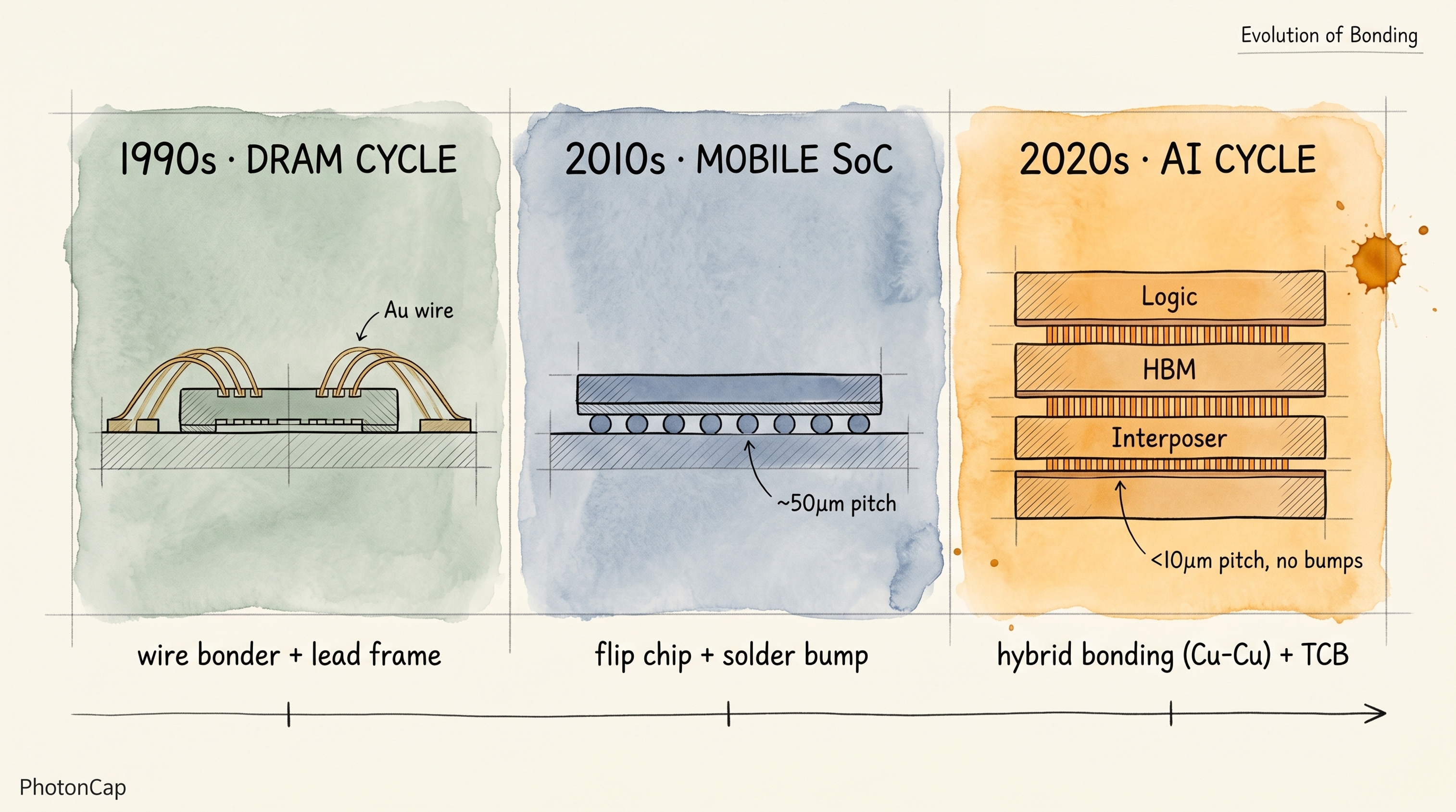
[Figure 1: Evolution of bonding by computing cycle, 1990s DRAM (wire bond) → 2010s mobile SoC (flip chip) → 2020s AI (hybrid bonding/TCB)]
The seven companies face very different cycle exposure. Two are bonding pure-plays at roughly $20B market cap each, with the highest beta. One is a $320B WFE giant whose bonding exposure is single-digit percentage of revenue but locks in a strategic ecosystem position. Two are diversified backend players where bonding sits as one segment among several. One is in transition from a wire bonder cash cow to fluxless TCB and HBM. One is private but is a standard-grade W2W bonder supplier and a peer valuation comp.
One-line takeaway: AI’s real chokepoint is not wafer fab capacity but advanced packaging bonding capacity. This article picks seven bonding equipment names directly exposed to HBM4, CPO, and photonic packaging cycles. Which seven, how they are split into four groups, and which one is most leveraged in which scenario are covered in the paid section.
2. Monolithic vs Bonding: two paths in the same fab
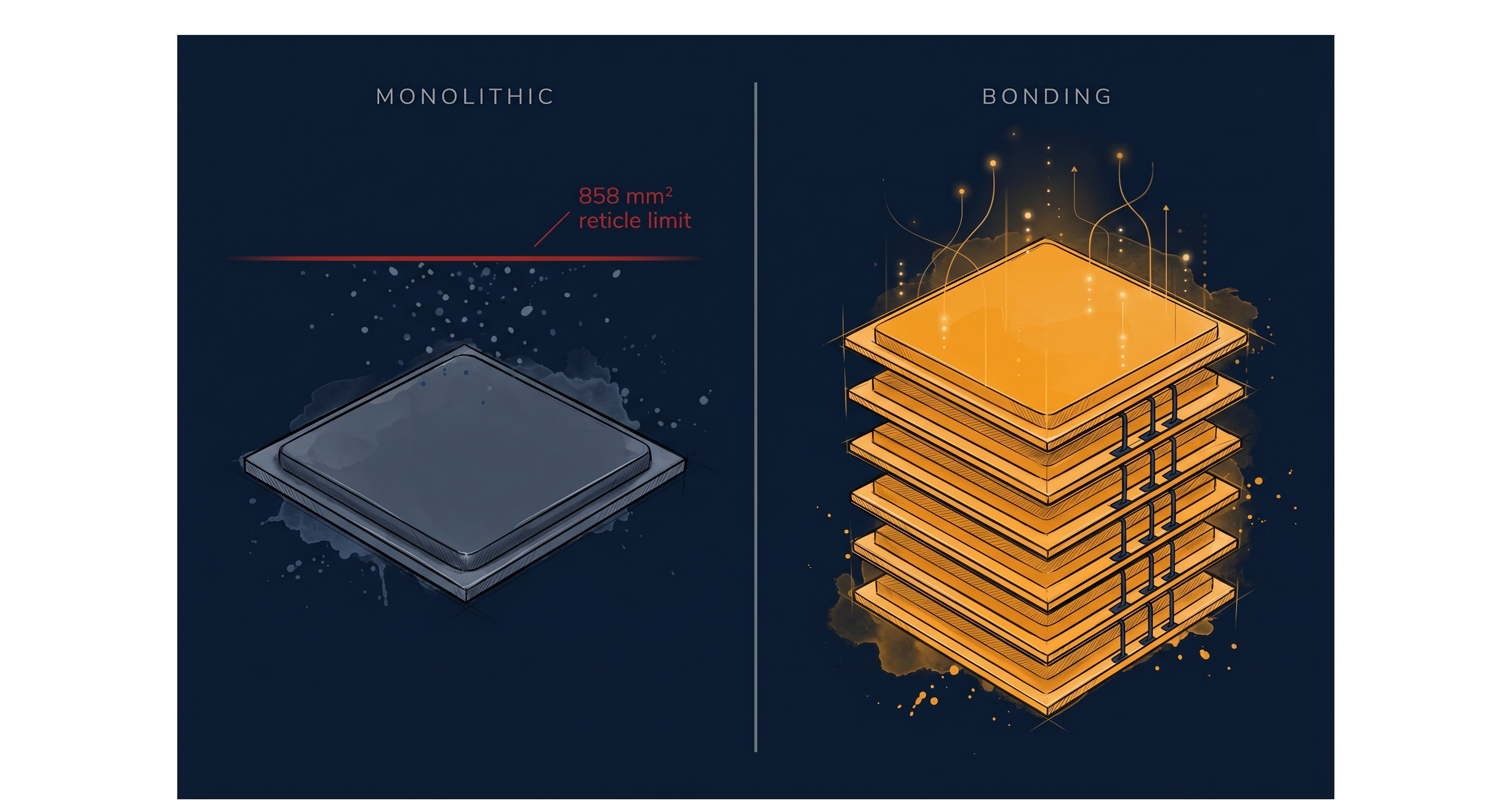
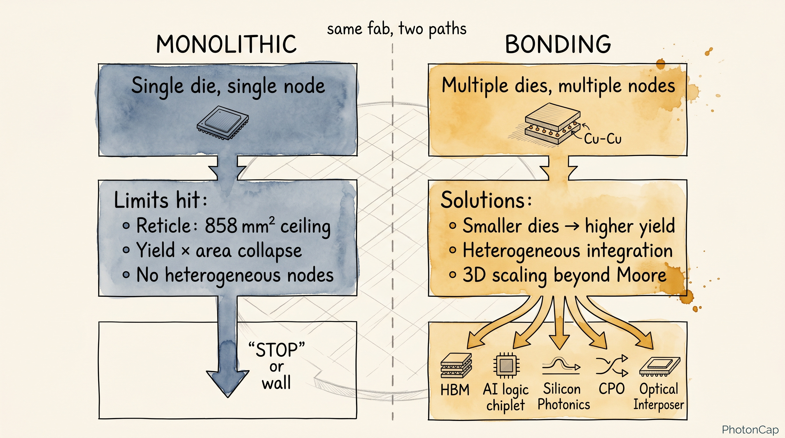
2.1 The limits of monolithic
Trying to fit everything onto one GPU die has already hit the reticle limit (about 858 mm²). Cramming logic plus memory plus I/O onto the same wafer node breaks down on both yield and cost. Whether it is NVIDIA Rubin, AMD MI400, or Apple M3 Ultra UltraFusion class SoC, leading-edge compute is moving away from monolithic single-die toward die-to-die integration and advanced packaging. HBM is even more dramatic. Going from 12-Hi to 16-Hi requires wafer thinning down to 30 μm [3], and packing 16 layers under the JEDEC HBM4 package height limit (775 μm) puts real pressure on the stack. Conventional micro-bumps and TCB are running out of margin, and hybrid bonding (Cu-Cu direct contact) is becoming an increasingly important option.
2.2 The bonding answer
Bonding fundamentally means “stacking different dies tightly together”. There are several techniques:
Wire Bonding: connecting chip pads to a lead frame with thin gold or copper wires. Used in legacy memory, automotive, and SMT for decades.
Flip Chip: flipping a chip upside down and joining it to a substrate via solder bumps. The standard for mobile SoCs and GPU substrates from the 2000s.
TCB (Thermo-Compression Bonding): melting micro-bumps with heat and pressure. Hits voids issues at fine pitch, evolving into fluxless TCB. The primary technique for HBM3E 12-Hi, partially extending to HBM4 12-Hi [4]. Tool price about $1-2M per system.
Hybrid Bonding: directly joining Cu pads to Cu pads at atomic level without micro-bumps, with the dielectric chemically bonded. Interconnect pitch comes down to sub-10 μm, and electrical and thermal characteristics are inherently better. Tool price about $3M, requires CMP step, demands higher cleanroom class [4]. Already used in AMD X3D, TSMC SoIC, and partially in HBM4 16-Hi.
[Figure 2: Monolithic vs Bonding comparison flowchart]
2.3 Two paths in the same fab
Same fab, two paths. Monolithic uses EUV / DUV lithography, etch, and deposition to print everything onto a single wafer. Bonding finishes individual dies on different wafers, then physically and chemically joins them. The two are not entirely substitutes (advanced logic chips still need monolithic for the base die), but bonding capacity is what determines the ramp speed of HBM stacks, AI chiplet integration, and photonic / CPO modules.
Worth noting: a front-end WFE giant has reached down into back-end bonding by acquiring a stake in one of the bonding pure-play companies, locking in one ecosystem axis [2]. Read in reverse, this means advanced packaging bonding is no longer a simple “back-end” step but an area as critical as wafer fab itself. Important enough that a front-end giant has to either enter directly or acquire. Which company acquired which, and what the ecosystem implication is, are covered in the paid section.
Key: same fab, two paths. Monolithic scaling is hitting reticle and HBM height limits, opening room for the bonding side. A front-end giant reaching down into the bonding pure-play ecosystem signals that bonding is now strategic territory.
3. Five domains where bonding lives
Bonding is not one market. It is five separate markets, where bonding requirements differ by precision, throughput, and process domain.
3.1 HBM memory stack
The current generation (HBM3E) splits in two. SK Hynix uses MR-MUF (Mass Reflow Molded Underfill), which reflows and underfills all layers in a single step [5], while Samsung and Micron use TC-NCF (Thermal Compression with Non-Conductive Film), pressing one layer at a time. SK Hynix took the lead on both yield and thermal performance, which translated into roughly 50% HBM market share advantage.
The next generation (HBM4) is going to 16-Hi, which requires wafer thinning to 30 μm to fit 16 layers under the JEDEC 775 μm height limit [3]. That is roughly half of the 50 μm used at the 12-Hi era. Three different paths emerge:
SK Hynix: keeping its MR-MUF strength as the primary path for HBM4 / HBM4E 12 to 16-Hi, while adopting hybrid bonding mass production in parallel for next-gen high-stack HBM (a two-track strategy). As of April 2026, SK Hynix has completed 12-high HBM hybrid bonding validation [35], and reportedly placed its first mass-production order for an inline hybrid bonding system co-developed by two global bonding equipment companies, at roughly KRW 20 billion [36]. This is moving past backup status into actual mass-production deployment.
Samsung: aggressive bet on hybrid bonding. As of April 2026, supplying 16-Hi HBM4 hybrid bonded samples to NVIDIA but with reported yields around 10% [3]. Hybrid bonding goes mainstream from HBM4E (2028).
Micron: continuing TC-NCF, with the largest hybrid bonding patent portfolio (180+ filings, Adeia IP license) [7].
There is one variable here. The JEDEC HBM4 standard was officially released as JESD270-4 on April 16, 2025, allowing 775 μm package height for both 12-high and 16-high (already loosened from HBM3E’s 720 μm) [41]. And on April 1, 2026, TrendForce reported (citing Newsis / Chosun Ilbo) that JEDEC is considering further relaxation to roughly 900 μm starting from HBM4E [6]. If this happens, the hybrid bonding timeline could slip by a generation. This is a variable that directly affects bonder ordering schedules.
On the equipment side, two companies hold TCB market share, one is targeting the next generation with hybrid bonding, and one has entered with fluxless TCB (first HBM system shipped to a large memory customer in December 2025) [8]. The exact identification table is in the paid section.
3.2 AI logic chiplet
This is one of the biggest current revenue drivers. AI accelerators increasingly depend on advanced packaging: Hopper-class GPUs already rely on large logic dies packaged with HBM, while Blackwell / Rubin-class platforms move deeper into multi-die integration. AMD MI300 / MI400 and X3D-class products make the chiplet and hybrid-bonding angle even more explicit. Across the board, leading AI compute chips are now built by bonding logic, memory, and I/O onto a single substrate or interposer.
TSMC effectively dominates this market with SoIC (System on Integrated Chips) and CoWoS (Chip-on-Wafer-on-Substrate), and CoWoS capacity is expanding toward 100,000 to 120,000 wpm by 2026 [4]. Intel runs its own line with Foveros Direct + EMIB, and Samsung Foundry is following with X-Cube.
AMD X3D (V-Cache memory die hybrid bonded onto a processor) is already a mass-production case using hybrid bonding [9]. An integrated D2W (Die-to-Wafer) inline line jointly developed by a front-end giant and a bonding pure-play is targeting high-volume manufacturing in this domain, and the D2W hybrid bonding market is estimated to grow from about $275M in 2025 to $2.4B+ in 2030 (CAGR 57%) [10]. Which two companies are behind this integrated line is covered in the paid section.
3.3 Silicon Photonics heterogeneous integration
This is the area where photonic chips (SiPh) and III-V light sources (GaAs, InP) get put on top of silicon. Monolithic absolutely cannot do this, so bonding is mandatory.
The classic heterogeneous integration example is bonding an InP laser onto a silicon photonics waveguide. Two global standard-grade suppliers (one listed, one private) hold positions in W2W (Wafer-to-Wafer) bonding for this domain [20], and one company supports silicon photonics CPO bonding via fluxless TCB [11]. Which company sits where is identified in the paid section.
3.4 CPO (Co-Packaged Optics)
This is the area where optical engines are co-packaged with switch ASICs / GPUs in the same package, replacing traditional pluggable optical transceivers. Reduces signal loss, lowers power, and increases bandwidth.
TSMC’s COUPE (Compact Universal Photonic Engine) platform was targeting 2026 production [12], and Samsung Foundry announced TC bonding-based OE (Optical Engine) for 2027 and CPO turnkey for 2029 [12]. NVIDIA Spectrum-X Photonics CPO switches, and Marvell / Broadcom CPO optical engines all fall in this category. NVIDIA has officially announced its own CPO switches, but the exact production split with external foundry platforms such as COUPE is reported by industry sources rather than formally specified, so it remains a monitoring item.
3.5 Optical Interposer (POET-class)
The newest category. Optical waveguides are drawn on a silicon or other substrate, with various optical and electronic chips bonded on top.
POET Technologies’ POET Optical Interposer is the representative case. A platform that integrates electronic and photonic devices (lasers, modulators, photodiodes, DSPs, etc.) into a single multi-chip module on a silicon interposer, with sub-micron precision die bonding as the core [13]. The business model itself sits on top of die bonding. If bonder capacity is short, POET’s commercialization speed is directly affected.
Lightmatter Passage falls in the same category. A 4,000 mm² active photonic interposer (GF Fotonix process) with logic chiplets stacked on top, creating in-package optical I/O [42]. Bigger than POET’s interposer and the logic chiplets are bonded directly on top, but the “bonding capacity = commercialization speed” structure is the same. Ayar Labs TeraPHY is structurally different. CMOS and photonic are monolithically integrated into a single die chiplet (also GF Fotonix-based), then co-packaged with the host SoC in the same multi-chip module package. This is chiplet-level co-packaging rather than stacking on an interposer, depending more on advanced packaging chiplet integration capacity than on bonding capacity [43].
Key: bonding is five separate markets, each requiring a different type of bonding and a different precision metric. No single company is #1 across all five.
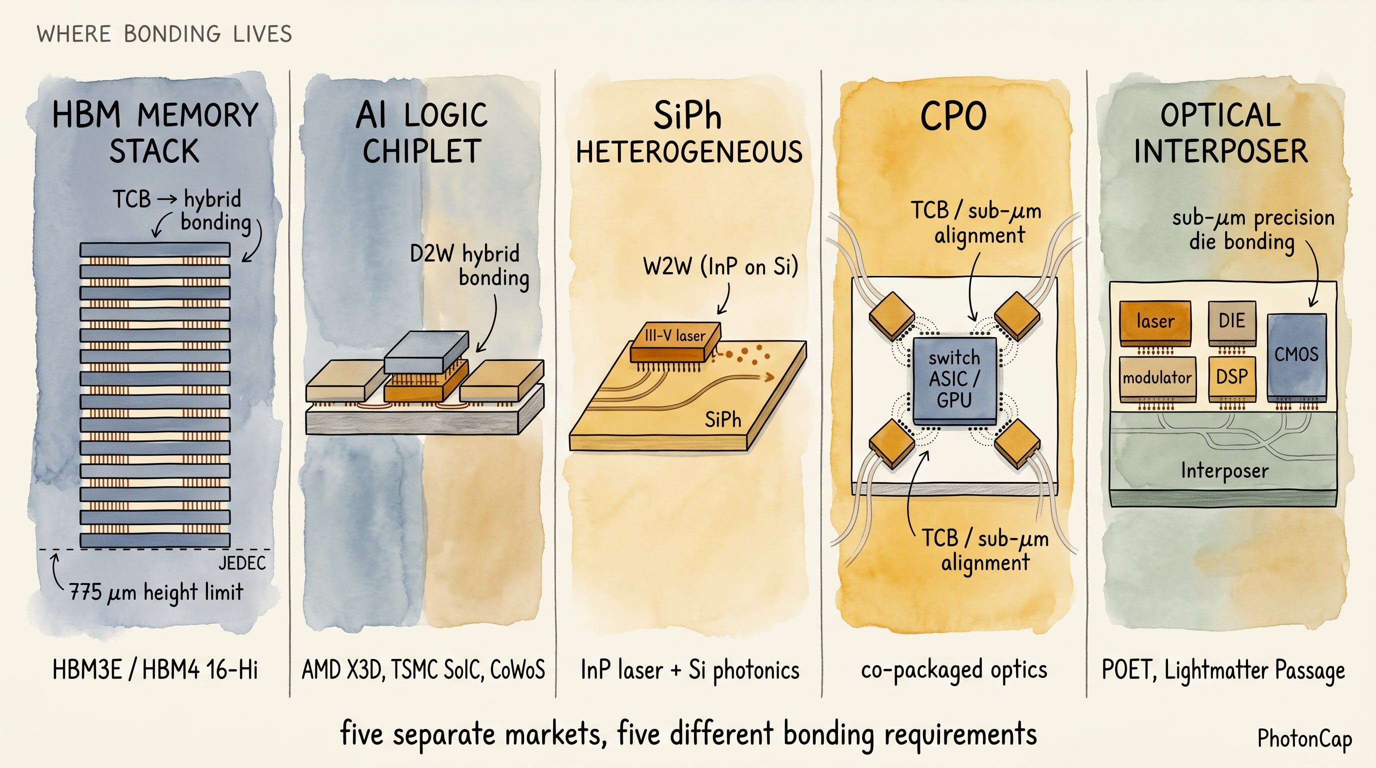
[Figure 3: The five domains where bonding lives. HBM memory stack, AI logic chiplet, SiPh heterogeneous integration, CPO, optical interposer in one visual]
4. Where the real divergence begins
The five domains above can be followed using public company disclosures. From here on, the real differentiation begins.
The bonding equipment market is converging on two specific events that will shift the whole picture over the next 12 months.
One is a takeover competition for one of the bonding pure-plays. According to a Reuters single-source report (London March 12, 2026 / NY March 13), one bonding pure-play company is evaluating takeover interest from two global WFE giants via Morgan Stanley, and that company’s stock hit an all-time intraday high of +14% the day of the report [14]. This is the biggest variable in bonding equipment ecosystem reshuffling. Rankings of the seven companies could shift by an order of magnitude depending on who acquires, or whether the deal falls through. Which company is the target, and which giant already holds a 9% stake, are covered in the paid section’s company-by-company analysis.
The other is JEDEC HBM4E height relaxation. According to TrendForce on April 1, 2026, JEDEC is considering further relaxation of the package height to around 900 μm starting from HBM4E (7th generation) [6]. If this happens, MR-MUF / TC-NCF could survive one more generation even at 16-Hi, and full hybrid bonding adoption gets pushed past HBM4E (2028). Samsung’s aggressive bet on hybrid bonding could turn out to be wasted, or could become a Samsung-only differentiation opportunity.
How these two cards affect each bonding equipment company, which company falls into which of the four groups, and which demand-side names locked into bonding (HBM 3 majors, AI compute, photonic, foundry) are most leveraged are the core variables for asymmetric positioning over the next 12 months.
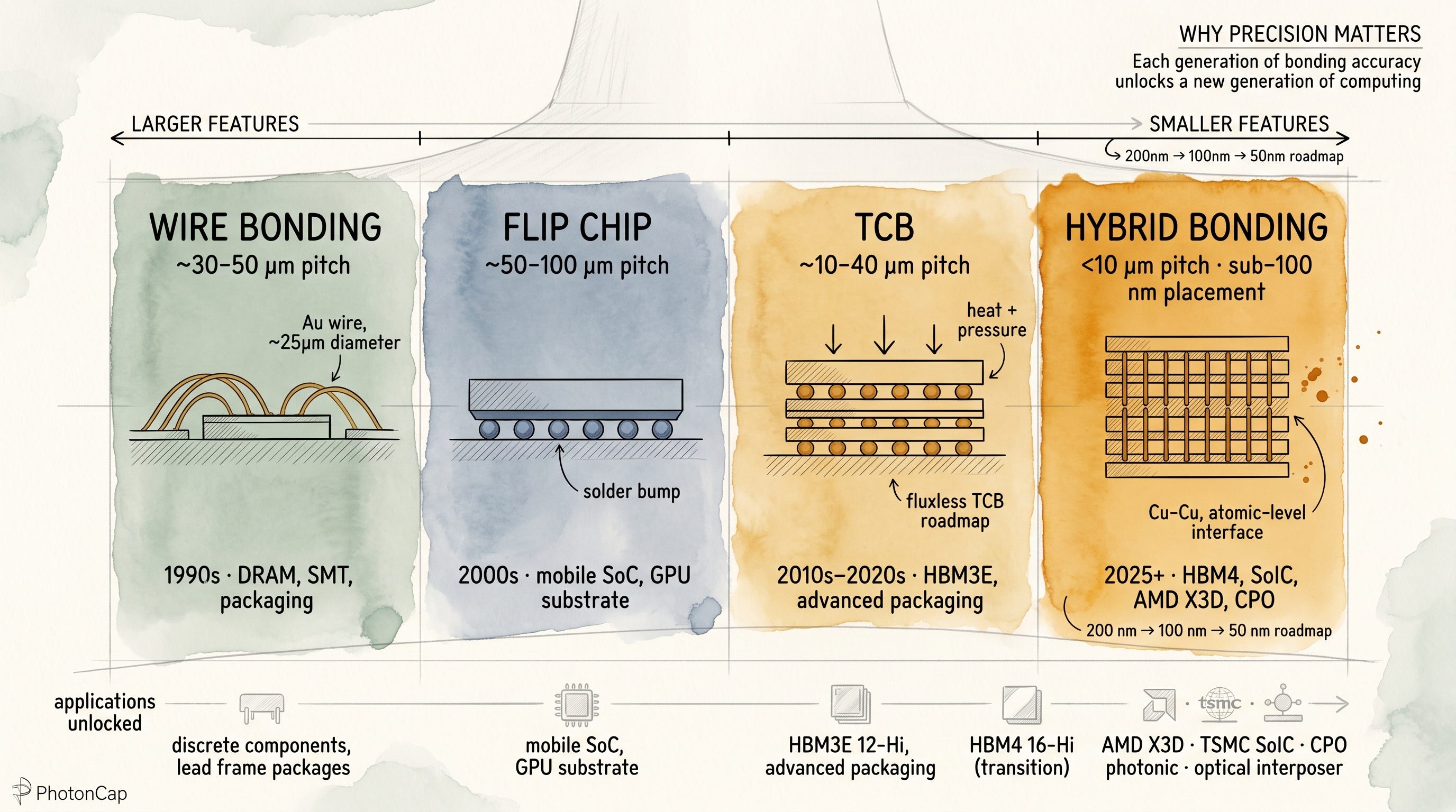
[Figure 4: Why precision matters, micron to sub-100nm progression and the applications it unlocks]