
On June 24, Qualcomm used its Investor Day to unveil HBC, an architecture that promises 133TB/s per card (vendor claim) with no HBM in it. Qualcomm presented Microsoft as its Azure deployment partner for HBC, while Meta’s name came attached to a separate multi-generation deal for the C1000 data center CPU. Around the same time, Nvidia put a LUT tensor core format that stores a weight in 3.125 bits into public documentation (the PTX ISA 9.4 developer preview) for the Rubin generation. The two approaches differ in direction but they are pounding on the same wall. The paradox, that every increase in HBM’s cost per byte improves the economics of designs that use less of it, has started showing up as hardware roadmaps and instruction sets. As I was wrapping this piece up on July 23, AMD and Cerebras announced a disaggregated inference partnership that splits prefill and decode across two different memory architectures, and on publication day itself, Samsung-Broadcom’s $200B+ MOU and SK Group-NVIDIA’s $500B+ LOI landed on top. This article audits the three bypass routes (distance, compression, pooling) one by one, and works out which direction each one pushes the DRAM makers and the optics timeline.
Related: $QCOM $NVDA $MU $AMD $CBRS
Contents
Intro: Hyperscalers Are Lining Up Behind a Company That Wants HBM Gone
Redefining the Memory Wall: Access Speed, Not Capacity
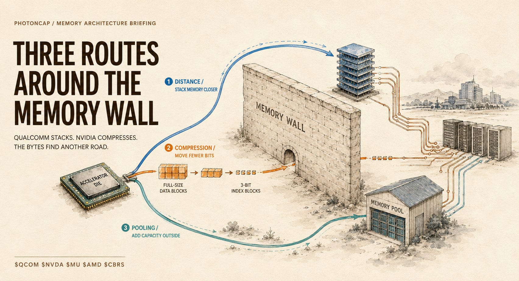
The Bypass Splits Into Three Routes
Route One, Distance: Auditing Qualcomm HBC
Route Two, Compression: Rubin’s 3.125 Bits
Route Three, Pooling: Why This Article Leaves It Alone
Stress-Testing the Samsung SiPh Thesis
The DRAM Makers’ Margin Mix Game
So When Does Optics Arrive
Scenarios and Monitoring
1. Intro: Hyperscalers Are Lining Up Behind a Company That Wants HBM Gone
A company declared it would take HBM out of the AI accelerator, and the CEOs of Microsoft and Meta showed up in its Investor Day program.
This was Qualcomm’s ($QCOM) Investor Day on June 24. The company laid out a data center roadmap with a target of more than $15B in data center revenue by FY2029 [1], and at the center of it sat an architecture called HBC, High Bandwidth Compute [2]. The idea is simple. Instead of HBM and an interposer, stack LPDDR directly on top of the accelerator die through TSVs. By Qualcomm’s own claims, a single AI250 card reaches 133TB/s, an 18x jump in effective bandwidth over the previous AI200 generation on LPDDR5X [2].
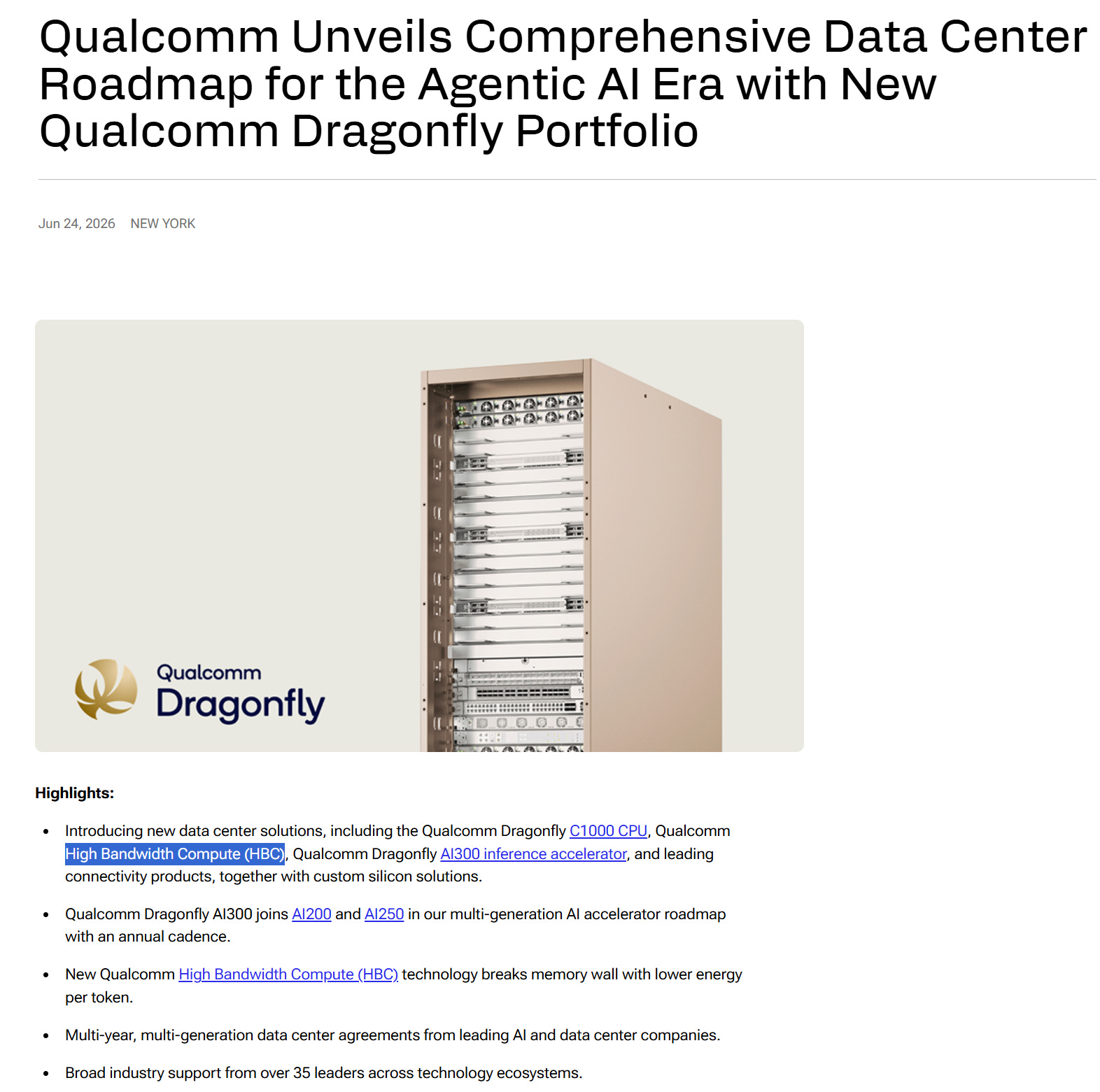
Whether those numbers survive contact with reality is a question for later (claimed and sustained performance are two different things, a principle I repeat every time a vendor announcement comes through). What matters first is the structural shift. Until now, “replacing HBM” lived in conference papers and startup slide decks. Now a top-tier semiconductor company is talking about it on an annual cadence roadmap, and hyperscaler names are attaching to it. The two names attach to different things, though, and they carry different weight. Meta’s side is a signed multi-generation deal, and its subject is not HBC at all but the C1000 data center CPU. Microsoft’s side is Qualcomm introducing the company as an Azure HBC deployment partner on the Investor Day stage [3], while Nadella’s own remarks read closer to an endorsement of the collaboration; Microsoft has disclosed neither deployment timing nor scale through its own channels. I will come back to this distinction, because blurring it means misjudging the size of the announcement. Most announcements these days work that way. The gap between the headline number and the actual scope of the contract is wide, and reading that gap is half the analysis.
A few weeks later, a move in a similar direction came from the opposite camp. The PTX ISA 9.4 document that Nvidia ($NVDA) released with the CUDA 13.4 developer preview carries a new tensor core mode for the Rubin generation (sm_107) [4]: a lookup table scheme that stores each weight as a 3-bit index rather than a value. The caveat is that this is still a preview document, not a GA release. The approach does not remove HBM. It shrinks the bytes you read out of it.
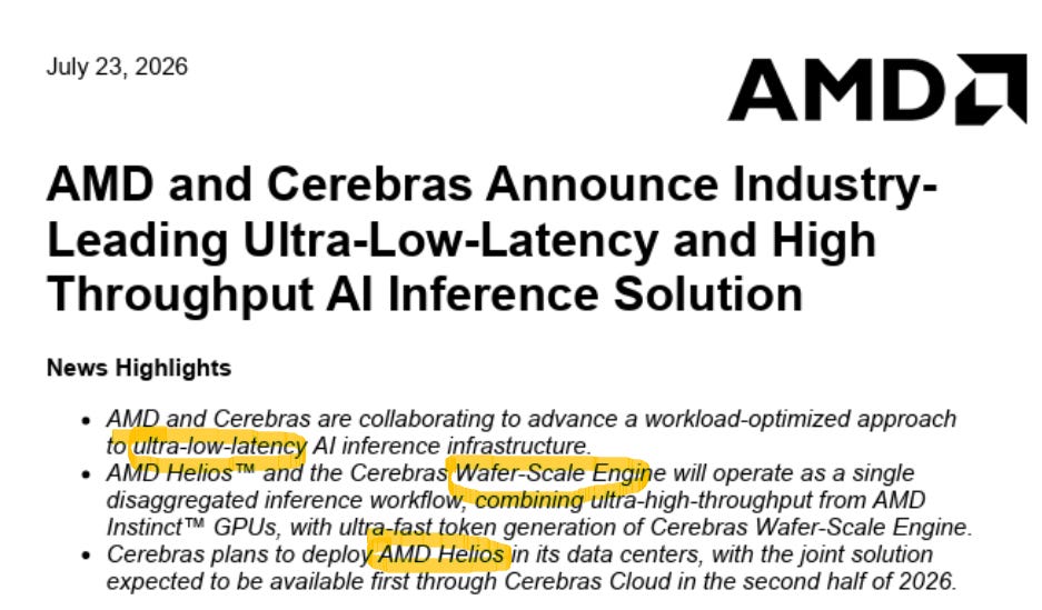
A third piece of hardware reality arrived on July 23, as I was closing this piece. AMD ($AMD) and Cerebras ($CBRS) announced a disaggregated inference partnership [5]. Prefill runs on HBM-based Helios racks, decode runs on the SRAM-based Wafer-Scale Engine (WSE). Two different vendors’ accelerators and memory architectures, announced as one joint inference solution. Availability starts in the second half of 2026 through Cerebras Cloud [5], and in that configuration, a single inference request travels between HBM and SRAM. SemiAnalysis, in its Advancing AI 2026 writeup published the same day as this piece, filed the deal as a strategy similar to the Nvidia-Groq arrangement [6], a sign that a shared pattern is forming across both camps rather than a single bypass.

Different companies, different layers of the stack, one bottleneck in the crosshairs, and a roadmap, an instruction set, and a commercial partnership all inside 30 days. Why now, of all times?
Two good pieces have already covered this 30-day window. Dylan Patel handled Rubin’s new tensor core from a benchmarking angle [7], and Citrini handled Qualcomm HBC from an incentive-structure angle [8]. Both are excellent, and neither references the other. One is an Nvidia piece and one is a Qualcomm piece, after all.

The framing that higher HBM prices raise the incentive for bypass architectures comes from the Citrini piece, and I first learned that Rubin carries a new tensor core mode from the SemiAnalysis piece. That much is borrowed. But reading the two side by side, something kept nagging at me. These bypass routes are different roads, so why does the same line item keep showing up at the end of every roadmap? And does the Samsung vertical integration thesis I laid out in an earlier piece survive this current? Neither article asks those questions, so I worked through them myself, recomputing the numbers from primary sources instead of either publication’s paid data. While I was at it, news kept piling up at a rate of one item every two days, so this piece includes things that broke on the morning of publication. I could not pick the timing, but the timing picked the material. Half of the writing turned into verification work as a result.
Key point: bypassing HBM is no longer a concept. In June and July 2026 it showed up as hardware: a roadmap ($QCOM HBC), an instruction set ($NVDA PTX ISA 9.4), and a commercial partnership ($AMD $CBRS), back to back.
2. Redefining the Memory Wall: Access Speed, Not Capacity
There is a principle this series keeps coming back to. The memory wall in LLM decode is an access speed problem, not a capacity problem. To be precise, that is the low-batch decode version of the story. As context grows and concurrent requests pile up, KV cache capacity climbs into the bottleneck too, and that branch gets its own treatment in chapter 6. (Previous piece: The Micron-Anthropic deal and the memory wall)
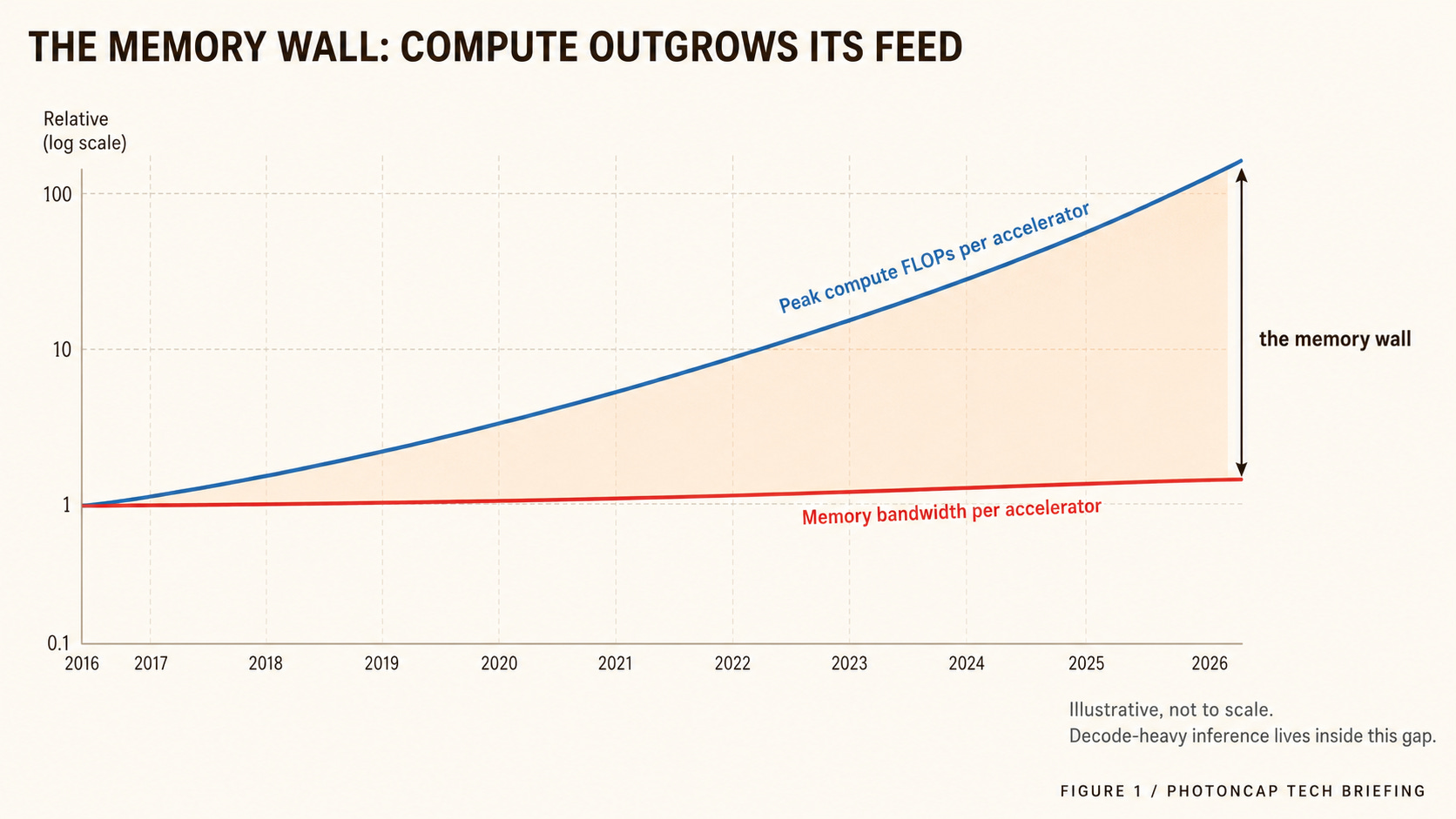
Figure 1: Compute FLOPs vs Memory Bandwidth Scaling Gap
Compute jumps every generation. The rate at which you can feed data into that compute does not keep up. The decode phase of LLM inference is where this bites hardest. In a dense model, producing each token means re-reading a large share of the weights (MoE reads mostly the active experts, so the total shrinks, but the character of the bottleneck, bytes per second, stays the same), and that is a job decided by memory bandwidth, not by FLOPs. The smaller the batch and the higher the interactivity requirement, the worse it gets. And with agentic workloads spreading, that is exactly the direction the market is demanding. An era that needs tokens fast, cheap, and nonstop is an era of decode, and decode’s bottleneck is the memory wall.
Think of a kitchen. Decode is a job where the chef (compute) spends most of the time fetching ingredients from the fridge (memory). However fast the chef’s knife gets, if the round trip to the fridge takes just as long, plates come out no faster. Over the past decade the industry doubled the speed of the chef’s hands every generation, while the fridge round trip did not manage half that pace. That is the memory wall. Hiring more chefs (adding compute) is not the answer. The plates are not late because of the knife work. Making the kitchen bigger (adding capacity) is not the answer to this particular problem either. The round trip is not slow because the kitchen is cramped. A bigger fridge (capacity) does not fix it. Speed up the trips, cut the number of trips per plate, or move the fridge next to the cutting board. Those three are the answers this article deals with. And all three share one trait: they get more serious as the fridge gets more expensive. The symmetry is worth remembering too. If fridge prices ever break, all three lose urgency together.
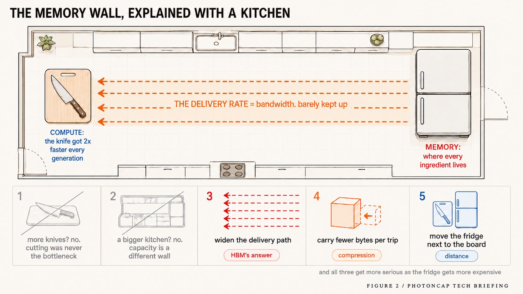
Figure 2: The Kitchen Analogy, the Memory Wall as a Round-Trip Problem
HBM is the current answer to this problem. Stack DRAM vertically, lay a wide bus through a silicon interposer, and buy your bandwidth that way. As answers go it has been excellent, and it remains the standard for frontier accelerators. It is also what drove the DRAM makers’ earnings and stock prices this cycle, and the reason this series has tracked advanced packaging all along. But the answer carries a price tag: silicon interposer and advanced packaging cost, power per stack, and above all, supply constraints. HBM is a product that only a few companies and a few lines can make, so when demand piles in, prices do not hold. And this cycle, demand kept piling in. Boil down two years of DRAM earnings calls into one phrase and you get sold out. The rule in this neighborhood is that the more successful the answer, the thicker its price tag gets. That thickened price tag is what you have been watching in the DRAM makers’ income statements. The very reason HBM became the biggest winner of the AI cycle is, to engineers, the incentive to find a way around it.
Let me say this up front: this is not an HBM-skeptic piece. HBM is still the most proven answer on the board. The question is about what comes next, the one created by that answer’s price. Problems born from an answer succeeding get solved differently than problems born from an answer being wrong.
High prices eventually summon their own cure. Usually the cure arrives as added supply. In semiconductors it can also arrive as a change of architecture. The higher HBM’s cost per byte climbs, the more relative value there is in a design that squeezes the same token out of fewer HBM bytes. Citrini Research flagged this incentive structure recently [8] (see Acknowledgment), and translated into this series’ frame it reads like this: if the diagnosis is right, if the memory wall is an access speed problem, then at the silicon and system level the fixes sort into raising access speed (the HBM road), cutting the bytes you must access (the compression road), or shrinking the access distance itself (the distance road). The model side has its own relief valves, GQA, speculative decoding, and so on, but this piece stays on silicon and systems. Each of those model-side techniques deserves an article of its own, and cramming them in here would do them no favors.
Key point: the HBM premium is itself the catalyst for anti-HBM design. If the problem definition (access speed) holds, the bypass narrows to three directions.
3. The Bypass Splits Into Three Routes
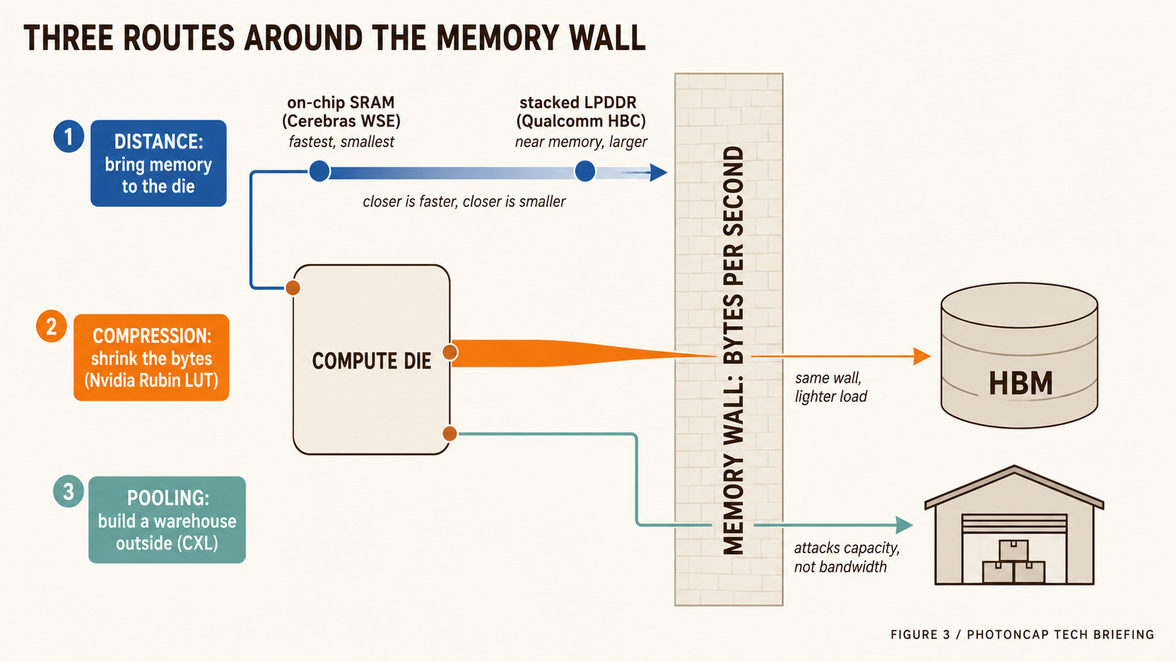
Figure 3: Three Bypass Routes Around the Memory Wall
The first route is distance. Cut or eliminate the distance data has to travel. This route is a spectrum, not a point. At the far end sits on-chip SRAM, memory placed inside the compute die itself (this is where Cerebras lives), and next to it sits Qualcomm HBC: LPDDR stacked in 3D on top of the accelerator, so data drops vertically through TSVs instead of crossing sideways over an interposer [2]. If HBC is moving the fridge next to the cutting board, SRAM is building the fridge into the board. Closer is faster, and closer is smaller. It would not be an exaggeration to say that trade-off is the whole story of this route. As we will see later, one commercial configuration announced this week demonstrates the trade-off like a textbook. Nor is it a coincidence that Qualcomm picked this road. This is a company that spent twenty-plus years getting squeezed by power and area budgets in mobile.
The second route is compression. Cut the amount moved rather than the distance. Rubin’s LUT tensor core lives here. Weights get stored in a low-precision format, but instead of plain rounding, a codebook-based non-uniform quantization gets reconstructed inside the MMA (matrix multiply-accumulate, the basic multiply instruction a tensor core executes) [4]. HBM stays, but the bytes flowing out of it shrink. This is not dodging the wall so much as lightening the load that hits it. It is also the next rung on the precision ladder that ran FP16 to FP8 to FP4, except this rung descends differently than the ones before it. How it differs is the subject of chapter 5.
The third route is pooling. Put another memory tier outside the accelerator and tie it in over an electrical interconnect like CXL. This route has a different character. In an era where long context and conversation history keep pushing KV cache out of HBM, the case for this warehouse gets clearer by the month. Where the first two routes attack bandwidth, pooling attacks capacity. Go back to the definition of the memory wall and this route is bypassing a different wall. As it happens, TrendForce started attacking that wall head-on this week, with a series on solving the KV cache capacity bottleneck through CXL expansion. Their split, capacity expansion versus footprint compression, lines up with this article’s map: their capacity expansion is the same road as my pooling, and their compression differs only in target. They shrink the KV cache; the compression in this article shrinks weights. I read it as a signal that the industry has started drawing the same map independently. Overlapping maps mean the direction is no accident. But the overlap ends at the map. Who is standing on which road, and how much each claim actually weighs, is where things diverge. Vendor slides, public instruction sets, and letters of intent are three different grades of evidence, and weighing them is what the paid section of this article does.

The three routes share a common backdrop. HBM pricing is what supercharged their economics. Each has its own drivers too, power, packaging capacity, latency, but if HBM cost half of what it does today, the gamble of stacking LPDDR on an accelerator, the acrobatics of packing weights into 3 bits, and the construction project of a separate warehouse would not be drawing this much investment. So the fate of these bypasses is not purely a technology question. It is also a function of the HBM price cycle. One DRAM price chart is enough to confirm the backdrop. You do not even need the chart; counting the recurring words in memory makers’ earnings releases will do. On the very day this piece goes out, two more announcements landed that cement that backdrop. Who got tied to whom, and what those ties mean for the bypass routes, gets sorted out later in the piece. Whether you buy DRAM or sell it, this map is not somebody else’s neighborhood.
That is as far as public information takes the map. But an investment decision needs more than a map. It needs an appraisal of each route. What conditions hang off Qualcomm’s 133TB/s? Where does the 3.125-bit figure come from, and how many percent of real HBM consumption does it actually remove? And above all, once the three routes have divided the workloads among themselves, what remains? The answers decide the DRAM makers’ margin mix, and they decide the timing of the package-level optics entry this series has been tracking. When the bypass grows, does optics get pushed out, or does it just change seats? I lean toward the latter, and the rest of this piece checks that lean one step at a time. The order: appraise the three routes, then set this series’ standing thesis on top of them, then come back to optics at the end. It is a long read, so if you are pressed, chapters 4 and 9 first, then circle back.
Let me show you one thing before the gate. Inside the very announcement that wants HBM gone, there is a section that looks like this.
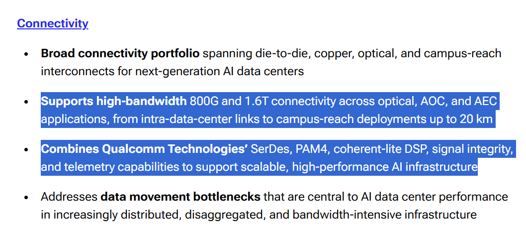
Screenshot 1: Qualcomm Dragonfly press release, Connectivity section, original capture with highlights / file: qualcomm_connectivity_screenshot.png / caption: “Source: Qualcomm press release, Jun 24, 2026”
800G and 1.6T optical, AOC and AEC, all the way to coherent-lite DSP [2]. A company removing HBM from memory put an optical connectivity portfolio in the same document, as its own separate pillar. Why this list is there, and what it means at the point where the three roads end, is the subject of this article’s final chapter.
4. Route One, Distance: Auditing Qualcomm HBC
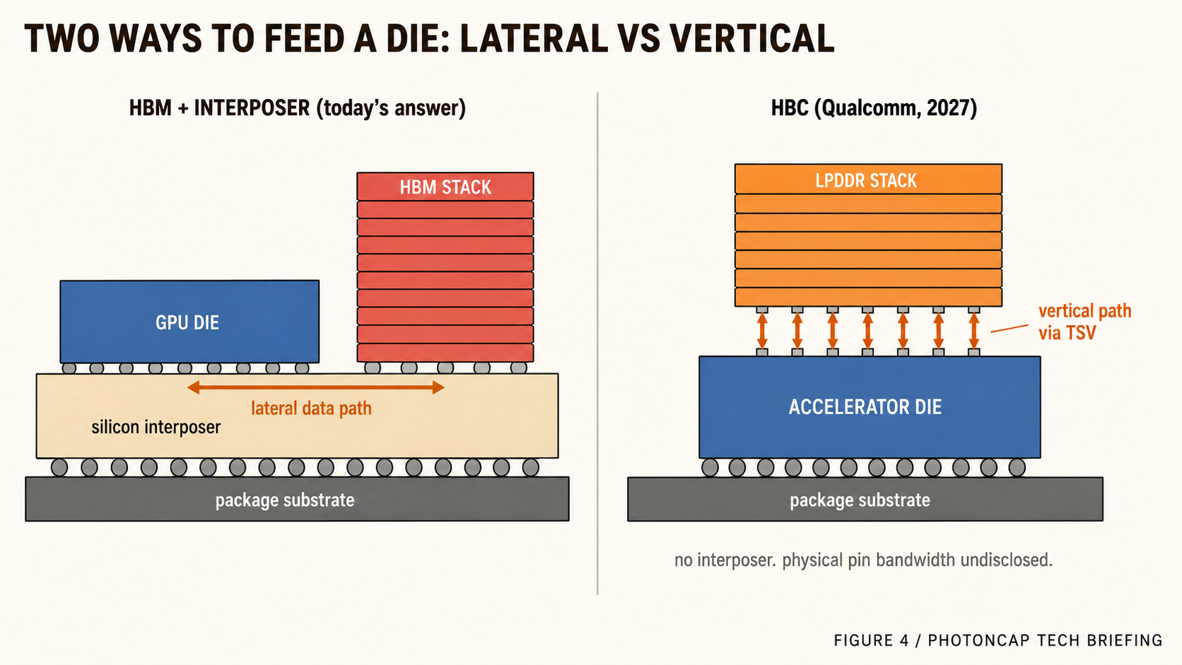
Figure 4: HBC Architecture vs HBM plus Interposer, Cross-Section View
