
TL;DR
The final prospectus SK hynix filed with the SEC for its US listing in July, and the 21 filings it has made since, never once mention “hybrid bonding” or “DRAM on logic.” Yet at the keynote of a forum the same company held in September, we heard that since this spring customers had started asking, almost as if on cue, for a structure that bonds DRAM onto a logic chip.
If this structure grows, the companies that buy hybrid bonders could change. It is a second source of demand that opened up while HBM bonding adoption slipped twice, a year each time, going by a bonder maker’s own timeline, and it is not yet settled whether the bonder purchase orders will go to memory makers or to foundries.
At the SK hynix Global Forum roundtable on September 18, the speaker said the slowdown in how fast HBM stack counts rise is a fact, but that it probably isn’t permanent. In effect, the question has moved from “how high do we stack” to “where do we stack.”
The difficulty with this structure lies in both design and process. Depending on whether the logic die goes on top or on the bottom, heat and power pull against each other; the DRAM needs a lower bonding temperature; and bonding whole wafers means the bad dies get bonded too.
Interestingly, when I lined up the public cases one by one, the line that decides who does the bonding turned out to lie somewhere other than foundry versus memory maker. My lead is that knowing that line lets you gauge who will buy the bonders, and that no matter who bonds or how, the XXXXX sector before and after bonding can’t be left out.
Contents
The Question of Whether 4-High or 8-High Is Enough
Is Stack Height Taking a Break?
Checking Against the Last Map
DRAM Comes Back on Top of Logic
Why the Bonding Is Hard
Who Stacks It
What to Watch on the Equipment Side
Closing
References
1. The Question of Whether 4-High or 8-High Is Enough
At the afternoon packaging roundtable of the SK hynix Global Forum, held in the US on September 18, HBM stack height came up in the later part of the Q&A. An audience member asked what the panel made of the recent talk that 4-high or 8-high HBM is optimal.
The speaker answered that a SemiAnalysis post from the previous week laid it out well. Its analysis is that as token counts grow, the sweet spot between bandwidth and capacity moves toward lower stack heights, and the speaker agreed with that analysis, saying the company’s own memory-systems people already know this. The speaker added that the steady rise in stack counts should be seen as having slowed a little, that this is simply where things stand for now, but that it probably isn’t permanent. The same answer went on to 3D stacking, putting DRAM on top of logic.
I read that answer as a sign that the question has moved. Since the speaker admitted the slowdown and denied that it is permanent, the question left is less how high to stack HBM than where to stack DRAM.
The official wording runs a little differently. In a post on the TSMC event published on September 28, the SK hynix newsroom wrote that HBM keeps raising its stack count and bandwidth with every generation, which makes close ties with packaging essential [1]. Put the company’s public wording next to the roundtable answer, and the picture is roughly of a company that isn’t giving up the stack-count race but is separately looking for what comes next.
The event was an invitation-only session that doubled as recruiting, so I didn’t get the slides. As in parts 1 and 2, every fact that carries a source number was checked against public material, and anything I only heard in the room is flagged as such. In part 1 I wrote that part 3 would be about who stacks and who buys the bonders. If DRAM goes on top of logic, who buys the bonders? Even if a memory maker supplies the DRAM, there’s no guarantee it also does the final bonding, and following the public stacking cases turns up some clues. After part 2’s 2.5D, this is the 3D story of stacking upward.
2. Is Stack Height Taking a Break?
Let’s start again from SK hynix’s public roadmap as laid out in part 1, SK hynix’s Four Packaging Paths: Where Is the Fight After HBM?. The roadmap slide shown again in the August 23 Hot Chips talk (its footer credits ISMP 2024) put 8-high and 12-high in mass production, 16-high in parallel development with improved MR-MUF and hybrid bonding, and 20-high and above at the research stage with hybrid bonding alone [2]. MR-MUF is SK hynix’s current method: it stacks chips with small bumps between them and then fills the gaps with a liquid protective material. Hybrid bonding joins copper pads directly, with no bumps.
The case for lower stacks was made by SemiAnalysis in a September 13 post [3]. Going by the free section, the gist is that in decode (the part of inference that generates tokens one at a time), cost per unit of bandwidth and cost per token are lowest at 4-high. Bandwidth per HBM4E stack is the same regardless of height, and by their own model, 8-high and 12-high cost a little over 10 percent and about 26 percent more, respectively, at the system level than 4-high, while throughput rises by 10 percent at most [3]. These are calculations for a specific rack and model, so I’d be careful about generalizing.
NVIDIA has published few official numbers so far. What NVIDIA has stated directly is only that Rubin uses up to 288GB of 12-high HBM4 per GPU [4]. For the next generation, Rubin Ultra, TrendForce reported in early August that NVIDIA had widened its evaluation to include 8-high HBM4E as well as 12-high and 8-high HBM4, and that the final spec had not been set [5]. Taiwan’s Commercial Times, citing a Morgan Stanley supply-chain survey, expected the spec to be set before the end of the third quarter [6], but as of September 28 I found no confirmed announcement or report. A figure of 192GB per GPU is also going around, but it is SemiAnalysis’s own reporting, and NVIDIA has never confirmed it [3].
In the roundtable talk, thickness came up first. The explanation was that within today’s thickness spec, 16-high and 20-high are close to the limit; going to 20-high or 24-high may need new technology, and another route is a large-area package that fills out capacity with more HBM stacks per package. Simply raising the stack count is a matter of setting an internal process baseline and qualifying it, the speaker said. With large-area packages, though, problems that never showed up in small packages surface in the bigger ones, and TSMC’s approach differs from other companies’, so each one has to be matched separately. We also heard that the DRAM die thickness in MR-MUF stacks started at 50 micrometers, which even people inside the company were skeptical about at the time, and is now close to 30 micrometers. If part 1’s 0.9x cut in chip thickness is the step for one generation, from 12-high to 16-high, this is progress built up over several HBM generations.
Here’s my view. SemiAnalysis’s 4-high logic is a calculation aimed at inference, and specifically at cost per token in decode, and the original piece itself acknowledges up front that pre-training is far more sensitive to capacity [3]. The speaker also said bandwidth and capacity trade against each other, so large capacity will be needed at some point. So I think that on the unit cost of decode alone, lower stacks win, but that capacity-hungry workloads could split off into a separate product line that uses taller stacks. Measured against the path laid out in part 1, the move to 16-high with existing methods has slowed a little, which is the opposite of 20-high and above being pulled forward.
3. Checking Against the Last Map
On September 17, when I ranked hybrid bonding equipment companies by score in [Investment Map] 22 Listed Companies in the Hybrid Bonding Value Chain, I judged that the stretch before memory adoption would be long and put a 1.5 weight on two scoring axes, logic and delay. Only eleven days have passed, so none of the dated checkpoints has come due, but when I pulled together the timing records behind that judgment again, they fit into a single table.
Starting with the 2024 records: an SK hynix packaging executive reportedly said at a November 2024 conference that hybrid bonding would be used from HBM4E, at a time when HBM4E mass production was planned for 2026 [7]. There was also an October report that Samsung Electronics had shown, at a 2024 conference, a roadmap applying hybrid bonding to HBM4 for mass production in 2026 [8]. Bonder maker BESI wrote in its 2024 Investor Day deck that memory adoption had slipped a year, to 2026 [9], and in this June’s deck it named 16-high HBM4E as the first insertion generation and wrote that a leading customer is preparing for high-volume manufacturing in 2027 [10].
Here’s where things stand now. Tom’s Hardware reported on the August Hot Chips talk that hybrid bonding would have a hard time making it into HBM4E, but according to the same article, the Hot Chips presenter didn’t name a target generation, and the company has not yet decided which product gets it first [11]. Two days later, a column by an Inha University professor published in the SK hynix newsroom judged that full adoption is most likely to come with HBM4E or HBM5 [12]. Market research firm Counterpoint expects SK hynix’s full-scale hybrid bonding production in 2029-2030, when HBM5 arrives [13]. Samsung said on its January earnings call that it plans partial commercialization at the HBM4E stage [14], and a July report said the company internally sees large-scale production becoming possible in 2030 [15].
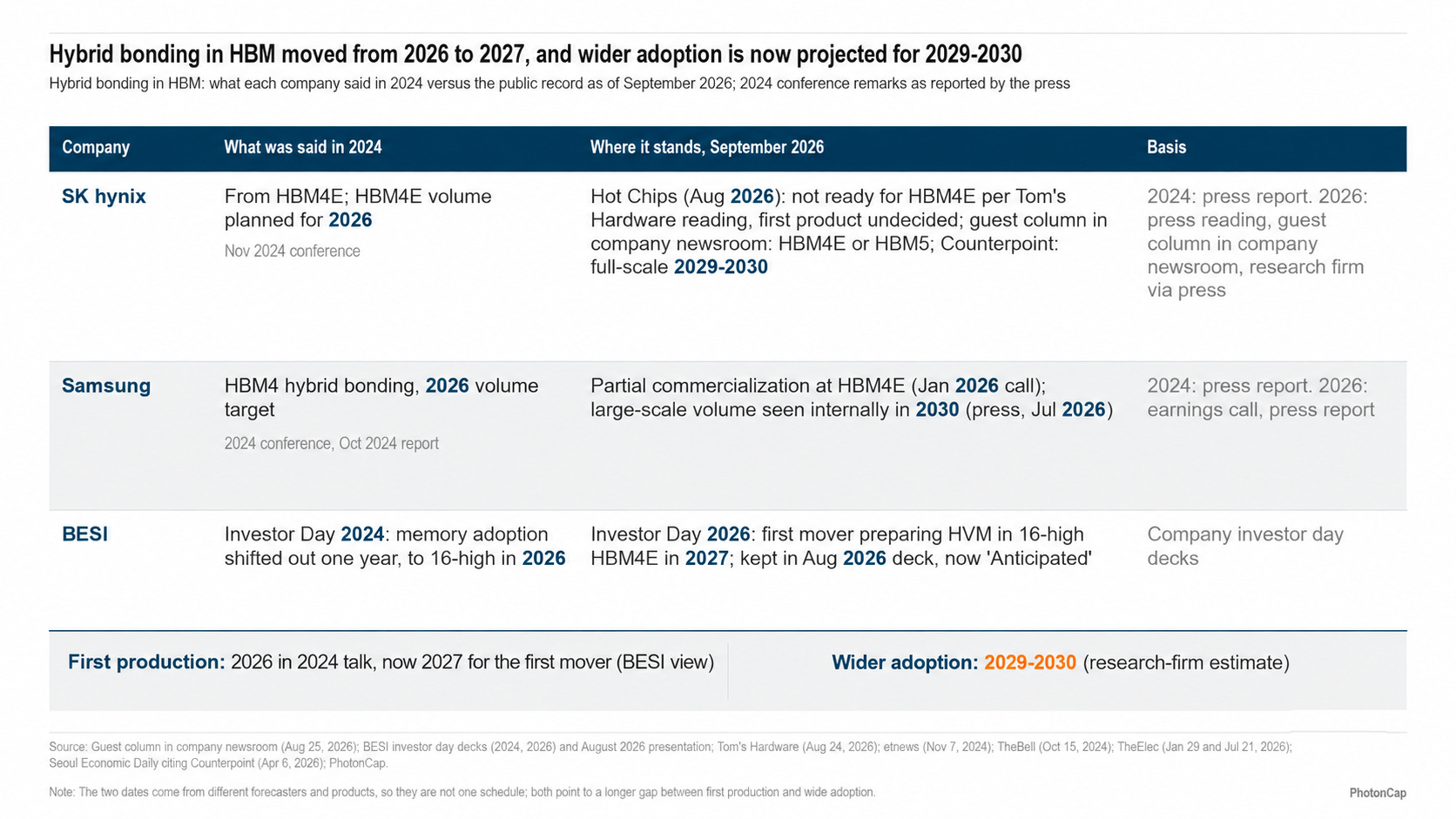
Hybrid bonding in HBM moved from 2026 to 2027, and wider adoption is now projected for 2029-2030. Table comparing each company’s 2024 roadmap with where it stands in September 2026
Put in a table, the records show that the 2026 both memory makers were naming in 2024 has become, in BESI’s reckoning, a leading customer’s 2027 production. BESI’s August deck kept that sentence and only added the word “Anticipated” to the title of its first-insertion slide [16]. The 2029-2030 date for wider adoption is a projection from market researchers like Counterpoint. Because the two numbers come from different forecasters and different products, they’re hard to tie into a single production schedule, but they point the same way: the gap between first use and wide adoption is getting longer. I spent a good while digging through 2024 conference coverage to fill this table, and the window when both companies were naming the same 2026 turned out to be shorter than I expected.
In my September 17 piece I read the Hot Chips talk as saying existing methods would carry through HBM4E. A guest column in the same company’s newsroom saw HBM4E or HBM5 as the likely entry point, and BESI is talking about a leading customer producing 16-high HBM4E in 2027. BESI’s third-quarter results on October 22 should give the first clue as to how those two line up. I’m leaving the 1.5 weight as is. When I pulled the evidence together again, the case that the gap to wide adoption is lengthening came out even firmer, so I’d say the call that the delay stretch would be long was right, to a degree.
4. DRAM Comes Back on Top of Logic
The roundtable speaker recalled that when the first generation of HBM was being developed, the structure the customer originally brought was 3D, but it ran too hot, so the design fell back to 2.5D. I mentioned this in part 1, and the reason that picture has come back is energy per bit. On a slide AMD showed in its ISSCC 2023 keynote, moving one bit of data costs about 12 picojoules for a memory module (DIMM), about 3.5 picojoules for HBM on an interposer (an intermediate substrate that holds the chip and the HBM side by side), and about 0.2 picojoules when chips are hybrid bonded one on top of the other [17]. In the panel discussion, too, we heard that trimming the energy spent on the interface circuitry (PHY) that DRAM and logic use to exchange signals under an agreed spec would raise efficiency. On the customer side, it’s just as the keynote remark in part 1 put it: since this spring, customers have started asking for this structure almost as if on cue.
At TSMC’s April symposium, SK hynix put 3D Stacked DRAM on Logic, which stacks DRAM vertically right on top of a logic chip, on its roadmap and wrote that it is particularly well suited to on-device AI [18]. The company’s public materials that I checked through September 28 give no year for this structure. The final prospectus filed with the SEC for the July US listing and the 21 Form 6-K filings since then don’t use the words “hybrid bonding” or “DRAM on logic” either; there is only a broad sentence about investing in custom base dies and advanced stacking techniques for next-generation HBM [19][20].
On why DRAM on logic is hard, the roundtable explanation was more concrete than the public material. From HBM4, SK hynix makes the base die on TSMC’s logic process, and it stacks the core DRAM on top with its own stacking technology, MR-MUF [21][22]. The speaker said this is closer to a minor change, moving a base die the company used to design itself onto a foundry design.
DRAM on logic is a different matter. According to the speaker, DRAM so far hasn’t used the low-k dielectric found in logic wiring (an insulating film with lower permittivity to cut signal delay); the process design changes completely depending on whether the logic die faces up or down; and the concepts behind aluminum pads and the layers that use low-k are different too, so there’s no way to know what problems will come up. We also heard that this only works if you open up information with your partners, down to the recipe level.
This much can be drawn from public material. In the paid section, I first walk through why this structure is hard from an engineer’s point of view, then put the public cases where DRAM has been bonded, or was announced to be bonded, onto logic into one table and compare who made the logic with who did the bonding. In the “who bonds” column of that table, only the SK hynix cell is empty, and how that cell gets filled will decide where the bonder purchase orders go. After that, I also lay out which process I’m watching instead of the bonders.
