
The 100-Second Bottleneck Behind NVIDIA CPO: 7 Companies That Own the 4-Stage Test Stack
FormFactor, ficonTEC, Advantest, Teradyne, Keysight, Chroma, Aehr: Mapping Companies to CPO Test Insertions

The bottleneck in CPO is no longer just “can you build the optical engine.” The bottleneck has shifted from fabrication to testing the PIC and optical engine at production speed. Per TrendForce, a full 100% optical inspection of a single CPO PIC takes over 100 seconds on average. With TSMC COUPE moving into production in 2026, the test equipment stack is emerging as a new supply chain choke point. This article breaks CPO testing into four insertions plus burn-in, and maps how FormFactor ($FORM), Teradyne ($TER), Keysight ($KEYS), Aehr ($AEHR), Advantest (6857.T), Chroma (2360.TW), and ficonTEC (private) each occupy their respective layers.
Contents
100 Seconds per PIC: Why CPO Test Is the Bottleneck
Background: The Physics of Why CPO Testing Is Hard
The 4 Insertion Framework and the Key Questions (paywall hook)
Insertion 1: PIC Wafer-Level Test
Insertion 2: EIC-PIC Combined Wafer-Level Test
Insertion 3: Optical Engine-Level Test, ficonTEC vs Chroma
Insertion 4: Module/System-Level Test
Burn-In: The Mandatory Step Outside the 4 Insertions
Two Competing Axes: Bull, Gap, Optionality
Scenario Analysis
Monitoring Points
Summary Table + Closing
References & Sources
1. 100 Seconds per PIC: Why CPO Test Is the Bottleneck
Per a recent TrendForce report, a full 100% optical inspection of a single PIC (photonic integrated circuit) going into a CPO module takes over 100 seconds on average.[1]
100 seconds. That is an order of magnitude longer than conventional semiconductor test. Over the past year, as this bottleneck became visible to the market, the equipment companies behind it moved at the opposite speed. One-year stock returns:
$AEHR +1,033%, Chroma (2360.TW) +757%, Advantest (6857.T) +389%, $FORM +468%, $TER +389%, $KEYS +150%. (as of 2026-05-06 close, price return basis, Yahoo Finance/Google Finance/Investing.com)
Market cap scales vary wildly. Advantest $128B, Keysight $62B, Teradyne $56B. These three are large-cap semiconductor equipment names. FormFactor sits at $11.6B, Aehr at $2.9B. ficonTEC is private (Germany-based, subsidiary of China’s Robo Technik). Chroma is listed in Taiwan at roughly TWD 979B (approximately $30B). Within the same CPO test ecosystem, market caps span orders of magnitude.
TSMC’s COUPE platform is entering CPO chip production in 2026.[1] NVIDIA invested $2B in Lumentum[2] and $2B in Coherent[3] to secure laser and optical networking capacity. A separate $2B strategic investment in Marvell covers NVLink Fusion, custom XPU, and silicon photonics/optical interconnect.[4] Across these three deals, $6B in AI connectivity and optics supply chain investment. Every one of these optical components needs to pass testing before it hits a production line.
Testing is becoming the single largest bottleneck in CPO mass production, and a competitive landscape is forming rapidly among equipment companies racing to solve it.
For context, consider the front-end equipment large caps. AMAT $327B, LAM $372B, KLA $236B (as of 2026-05-06). Against this group, CPO test companies sit at a distinctly different scale. Keysight ($62B), Teradyne ($56B), and Chroma (~$30B) are large test and measurement companies, but still 5 to 12 times smaller than front-end equipment leaders. FormFactor ($11.6B) and Aehr ($2.9B) are one to two orders of magnitude smaller. If CPO test grows into a multi-billion-dollar annual market comparable to front-end equipment, the market cap gap for pure-play smaller names like FormFactor and Aehr could be due for reassessment. The opposite is also possible. If CPO production gets delayed, test equipment capex gets deferred with it.
FormFactor reported Q1 2026 revenue of $226.1M (+32% YoY), beating guidance, and raised its 2026 CPO revenue guide to the high end of the $10-20M range on its earnings call.[5][6] Teradyne reported Q1 2026 revenue of $1.282B (+87% YoY), with AI-related revenue accounting for roughly 70% of the total.[7] Aehr disclosed a record $41M order from a hyperscale AI customer in April 2026 (for custom AI processor ASIC package-level burn-in).[8] None of these data points existed a quarter ago.
FormFactor Q1 2026: SK hynix 29.5%, NVIDIA 10.2%, and the First CPO Test Revenue Signal

Three cycles bent together in a single quarter at FormFactor (FORM) Q1 2026. SK hynix reached 29.5% of revenue (up from 23.3% a year ago), NVIDIA was disclosed as a 10%+ customer for the first time at 10.2%, and 2026 CPO revenue guidance was raised to the high end of the $10-20M range. Revenue hit $226.1M, an all-time record (+32% YoY), with Q2 guidance at $240M. The stock returned +361% over one year, roughly 2.7x the semiconductor index (SMH, +134%). The thesis the market had been pricing in for a year was confirmed in a single quarter’s numbers. This article breaks the earnings into three axes, HBM, CPO, and AI networking, and analyzes the alignment and risk across them.
Bottom line: 1Y returns for the 7 CPO test equipment companies range from +150% to +1,033%. Market caps range from $2.9B to $128B. Compared to front-end equipment large caps (AMAT/LAM/KLA at $236B to $372B), pure-play names like FormFactor ($11.6B) and Aehr ($2.9B) are one to two orders of magnitude smaller. The speed at which NVIDIA’s $6B AI connectivity investment converts to actual production volume will define the next 12 months for these companies.
2. Background: The Physics of Why CPO Testing Is Hard
Start with why it takes 100 seconds.
A single-mode fiber core has a cross-sectional area of roughly 78.5 square micrometers. A silicon photonic strip waveguide is roughly 0.099 square micrometers. That is an 800x difference. Bridging this gap requires nanometer-precision alignment to couple light in and out of the device under test. Much of this process is still partially manual. There is no unified industry standard.
Conventional semiconductor test only deals with electrical signals. Touch the probe card to the pads and you are done. SiPh/CPO test requires simultaneous electrical and optical probing. You drive the modulator with electrical signals while simultaneously coupling light through an optical coupler, then receive the modulated optical signal on the output side. This requires six or more axes of precision positioning, with alignment tolerances in the tens of nanometers.
Add 3D hybrid bonding (the TSMC COUPE architecture) and it gets worse. When PIC and EIC are bonded face-to-face, the optical coupler ends up on the bottom side of the wafer. Electrical contacts are on top. You need to probe from both sides simultaneously. Existing semiconductor test equipment cannot do this.
From the perspective of established equipment companies, this is a completely different technology stack from the deposition, etch, and metrology tools that AMAT, LAM Research, and KLA ($200B to $370B market caps) dominate. In conventional wafer test, probe card pin placement accuracy at the micrometer level is sufficient. SiPh optical coupler alignment tolerance is in the tens of nanometers, roughly 100 times more stringent. Factor in thermal expansion from temperature changes (silicon CTE is roughly 2.6 ppm/K) and you cannot simply bolt an optical module onto an existing probe station. You need equipment designed from scratch for optical alignment.
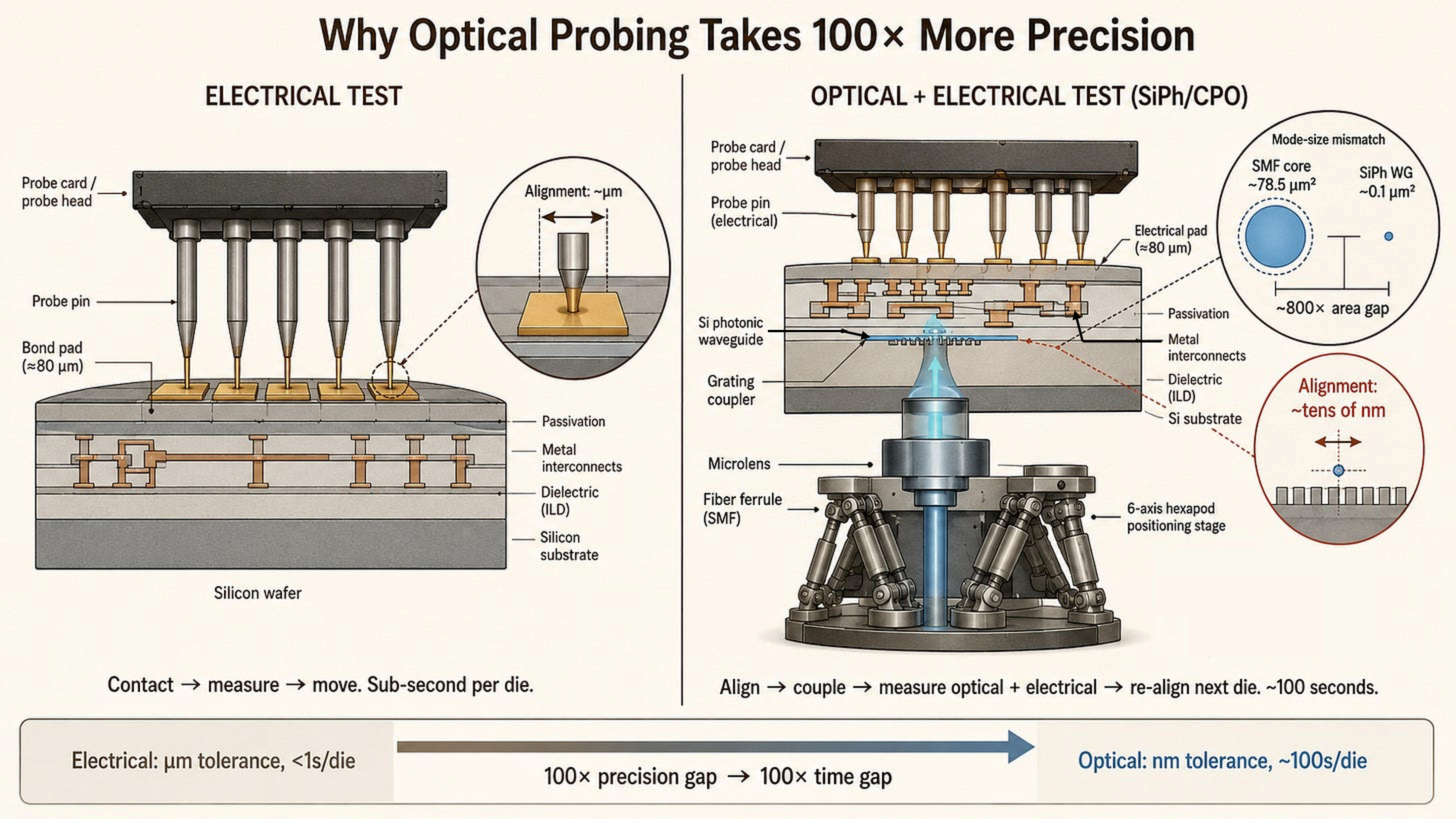
[Figure 1: Electrical vs Optical Probing Comparison, Mode Size Mismatch]
There is another issue. Conventional electrical test has high repeatability. Align the probe card once and you can automatically test the entire wafer. In optical test, coupling conditions change from die to die. Waveguide position, edge coupler angle, and grating coupler pitch all carry process variation at the die level, so optical alignment must be independently optimized for each die. This accounts for a significant portion of the 100 seconds. FormFactor’s claim of sub-5-second per-die test time on the CM300xi-SiPh is a data point showing progress in alignment automation.[9] That said, TrendForce’s “100 seconds” and FormFactor’s “sub-5 seconds” likely refer to different test content scopes. The 100 seconds appears to cover full optical inspection, while the 5 seconds likely refers to alignment plus basic parameter measurement for a specific recipe. Direct comparison requires caution.
This is why the CPO test market is being driven not by the existing equipment large caps, but by these seven companies with specialized capabilities in photonic probing, optical alignment, and burn-in.
Previous PhotonCap and Damnang articles covered this technical background in detail:
Why SiPh wafer test is hard, and how AEHR, FormFactor, and Keysight each cover a different layer: “The Three Pillars of SiPh Wafer Test”[9]
Three signals from FormFactor’s Q1 2026 earnings (SK hynix 29.5%, NVIDIA 10.2% first 10% disclosure, CPO revenue high-end guide), plus TRITON production entry, Keystone acquisition, Teradyne Photon 100 competition: “FormFactor Q1 2026”[5]
FormFactor Q1 2026: SK hynix 29.5%, NVIDIA 10.2%, and the First CPO Test Revenue Signal
·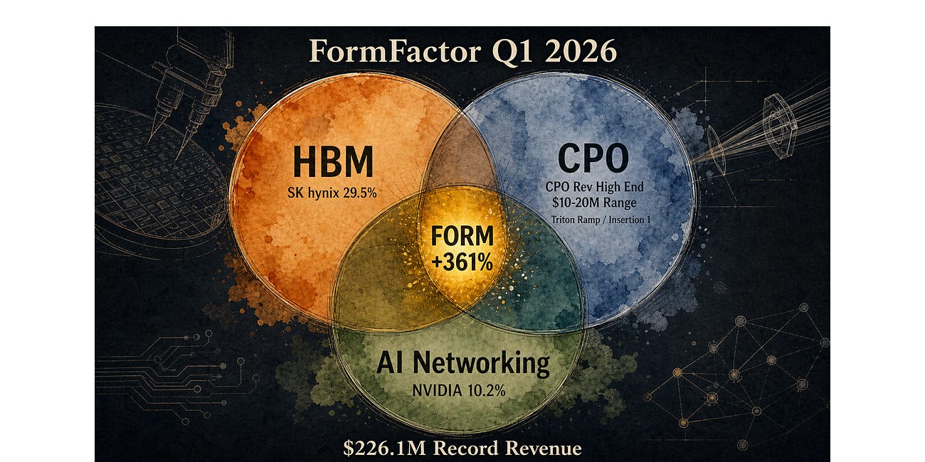
Three cycles bent together in a single quarter at FormFactor (FORM) Q1 2026. SK hynix reached 29.5% of revenue (up from 23.3% a year ago), NVIDIA was disclosed as a 10%+ customer for the first time at 10.2%, and 2026 CPO revenue guidance was raised to the high end of the $10-20M range. Revenue hit $226.1M, an all-time record (+32% YoY), with Q2 guidance at $240M. The stock returned +361% over one year, roughly 2.7x the semiconductor index (SMH, +134%). The thesis the market had been pricing in for a year was confirmed in a single quarter’s numbers. This article breaks the earnings into three axes, HBM, CPO, and AI networking, and analyzes the alignment and risk across them.
F2C assembly companies in CPO optical packaging: PC101 Lecture 4 Part 2[10]
[PC101] Lecture 4: The Last Millimeter: Who Builds It. CPO Packaging Value Chain and Next-Gen Applications (Part 2)
·![[PC101] Lecture 4: The Last Millimeter: Who Builds It. CPO Packaging Value Chain and Next-Gen Applications (Part 2)](https://substackcdn.com/image/fetch/$s_!t--v!,w_1300,h_650,c_fill,f_auto,q_auto:good,fl_progressive:steep,g_auto/https%3A%2F%2Fsubstack-post-media.s3.amazonaws.com%2Fpublic%2Fimages%2F79e1619c-b4a2-43cc-a8b9-8718a9c256c5_4894x2739.png)
Welcome back. This is PhotonCap.
Seven bonding equipment companies accelerating across HBM4 and CPO cycles: “Seven Bonding Equipment Companies”[11]
7 Bonding Equipment Companies Behind HBM4 and CPO: AI’s Real Bottleneck Lives in Assembly
·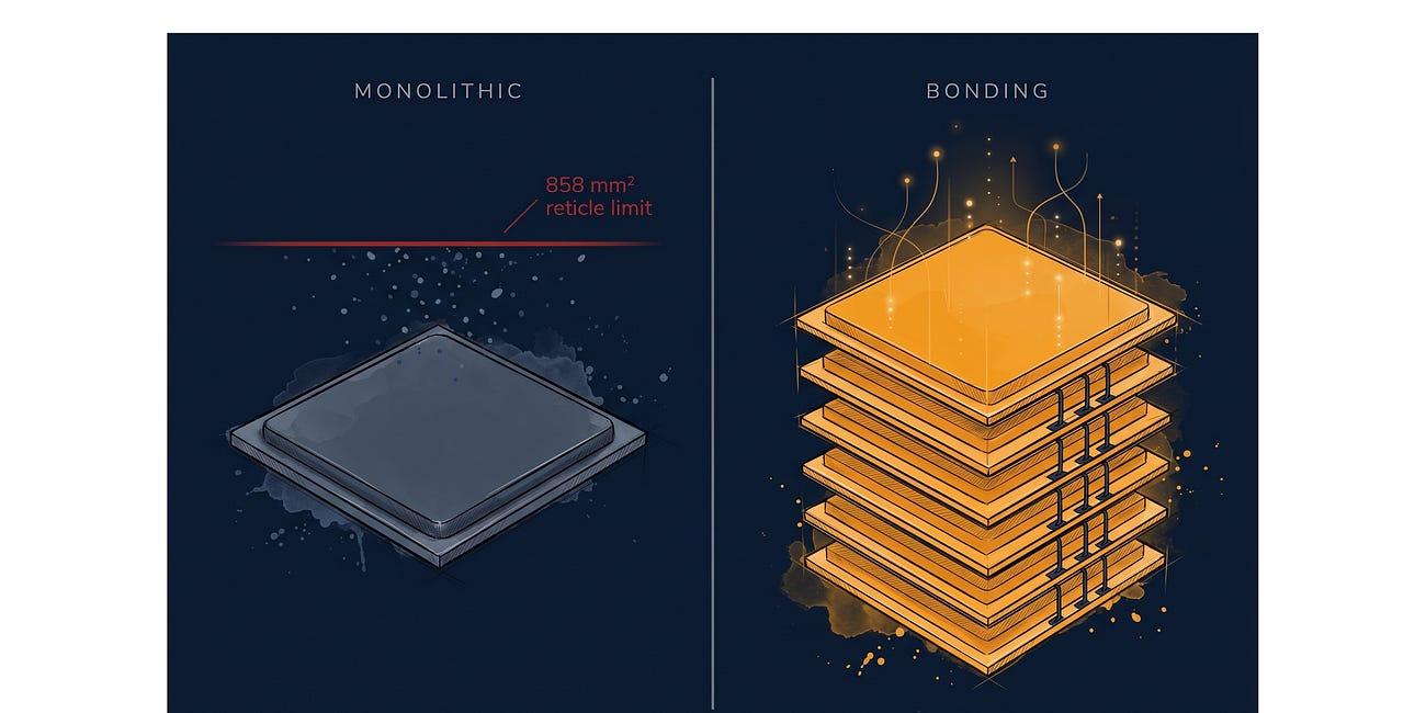
Computing cycles have always split at “assembly”. The 1990s DRAM cycle was won at the wire bonder. The 2010s mobile SoC era was won at flip chip. The current AI cycle is moving to hybrid bonding (Cu-Cu direct contact) and TCB (thermo-compression bonding). With monolithic scaling effectively halted at the reticle limit, bonding has become the new path forward, and HBM4 plus co-packaged optics (CPO) packaging capacity has become a real bottleneck. This article maps seven bonding-equipment names most directly exposed to that bottleneck, the five bonding domains they sit in, and which scenarios most concentrate the asymmetry. Two of the seven are bonding pure-plays with nearly 100% bonding revenue. Two are absorbing current-cycle TCB cash flow. Two carry photonic / W2W option value. One is in transition from a wire bonder core to advanced packaging. The identification table, order-of-magnitude comparison, differentiation table, and company-by-company analysis are in the paid section.

![[PC101] Lecture 4: The Last Millimeter: Who Builds It. CPO Packaging Value Chain and Next-Gen Applications (Part 2)](https://substackcdn.com/image/fetch/$s_!t--v!,w_1300,h_650,c_fill,f_webp,q_auto:good,fl_progressive:steep,g_auto/https%3A%2F%2Fsubstack-post-media.s3.amazonaws.com%2Fpublic%2Fimages%2F79e1619c-b4a2-43cc-a8b9-8718a9c256c5_4894x2739.png)


This article builds on that technical foundation. The scope here is mapping the 4-stage CPO test insertion structure and identifying which companies occupy which roles at each stage.
One more piece of context. CPO test market growth is not simply proportional to CPO chip shipments. Longer test times mean more equipment is needed. Testing 1 million PICs at 100 seconds each requires 100 million seconds, roughly 27,778 equipment-hours. At 24-hour operation and 85% uptime, a single test cell processes roughly 734 PICs per day, or about 22,000 per month. 100,000 per month requires roughly 5 single-site test cells. 1 million per month requires roughly 45. Add retesting, multiple insertions, and multi-engine architectures, and actual equipment demand exceeds these figures. The equipment competition is a test time compression competition. The company that cuts 100 seconds to 50, then to 25, can serve the same customer volume with less floor space and capex. This is why FormFactor emphasizes per-die test time reduction and ficonTEC pushes multi-site parallel testing. Throughput competition is the equipment market competition.
Bottom line: The fundamental reasons CPO test is hard are simultaneous electrical plus optical probing, nanometer alignment, and double-sided access. 100 seconds of test time per PIC directly determines how many production test cells are needed. These technical requirements open the market to specialized companies rather than the existing equipment large caps.
3. The 4 Insertion Framework and the Key Questions
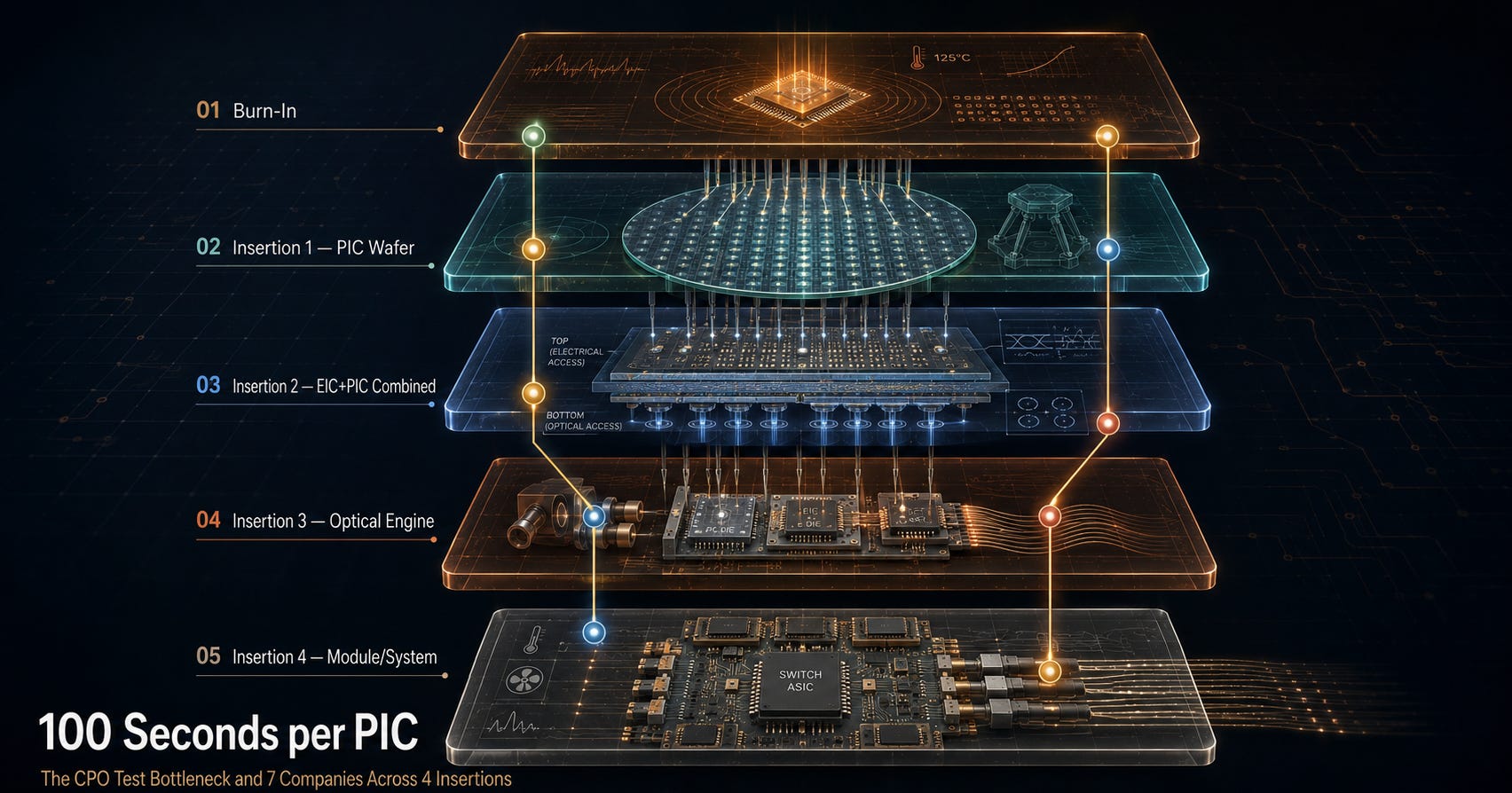
CPO testing is divided into four test insertions, from wafer to system.[12]
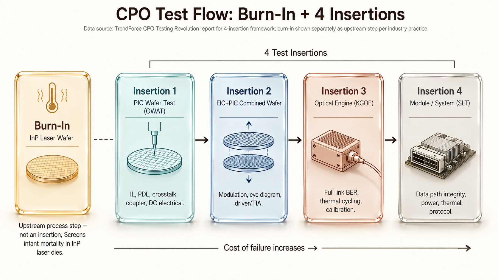
[Figure 2: CPO Test 4 Insertion Flow Diagram]
Outside this four-stage framework, there is one more step. Burn-in. This is the process step that screens for infant mortality in InP lasers, performed before Insertion 1.
Everything up to this point is visible from public data and the TrendForce report. Four insertions, plus burn-in as a separate step. You can figure this out from industry conference slides and equipment company press releases.
The real differentiation starts here.
These seven companies form two distinct competing axes within the four insertion stages, with the remaining companies classified as cross-axis layer players that are not tied to either axis. The technical strengths and weaknesses of each axis are precisely inverted.
As a subscriber asked, are ficonTEC and Chroma competitors or coexisting at Insertion 3? The answer becomes clear once you understand the two-axis structure.
One more thing. One of these seven companies has a Chinese ownership structure. With CPO test becoming a choke point in production, how this structural risk could influence customer vendor selection is covered in the paid section below.
The paid section below breaks down the test station structure for each insertion and maps Bull/Gap/Optionality for each axis. How each axis’s technical strength can flip into a weakness under specific conditions, and why cross-axis layer players remain relatively stable regardless of scenario, with quantitative data.
Do the order-of-magnitude differences in market cap among these seven companies reflect their actual positioning in the CPO test market, or is the market still mispricing them? The answer requires understanding the insertion-by-insertion landscape first.
One preview: the most interesting point of competition between the two axes is not technology. It is corporate structure. How one axis’s key partner’s ownership structure could distort customer vendor selection may be the most underpriced variable in the investment equation. Especially in the current environment where US-China technology competition is extending into the semiconductor equipment supply chain.
