
[PC101] Lecture 4: The Last Millimeter: Who Builds It. CPO Packaging Value Chain and Next-Gen Applications (Part 2)
— Who Packages the Light: Bottlenecks and Opportunities in the F2C Value Chain —

Welcome back. This is PhotonCap.
In Part 1, we looked at the 1,000x mode mismatch between optical fibers and chips, then compared six coupling techniques (edge, grating, evanescent, freeform, cantilever, and photonic wire bonding) and their trade-offs.
[PC101] Lecture 4:The Last Millimeter: Fiber-to-Chip Coupling and the CPO Packaging Bottleneck (Part 1)
![[PC101] Lecture 4:The Last Millimeter: Fiber-to-Chip Coupling and the CPO Packaging Bottleneck (Part 1)](https://substackcdn.com/image/fetch/$s_!qZxp!,w_1300,h_650,c_fill,f_webp,q_auto:good,fl_progressive:steep,g_auto/https%3A%2F%2Fsubstack-post-media.s3.amazonaws.com%2Fpublic%2Fimages%2Fa743aebb-02e3-496d-95cf-0da2962050b1_3590x2099.png)
Welcome back. This is PhotonCap.
Part 2 widens the lens. “Who is packaging CPO, with what F2C (Fiber-to-Chip) technology, at which foundry, and with which components?” We map the entire value chain. We compare the coupling choices behind NVIDIA, Broadcom, and Marvell’s CPO switches, examine how four foundries are baking F2C into their process flows, trace why M&A is accelerating in this space, and walk through the real-world assembly challenges of photonic vias, glass substrates, epoxy shrinkage, and thermal stress.
Section 9 (CPO architecture comparison) is free. Section 10 onward is for paid subscribers.
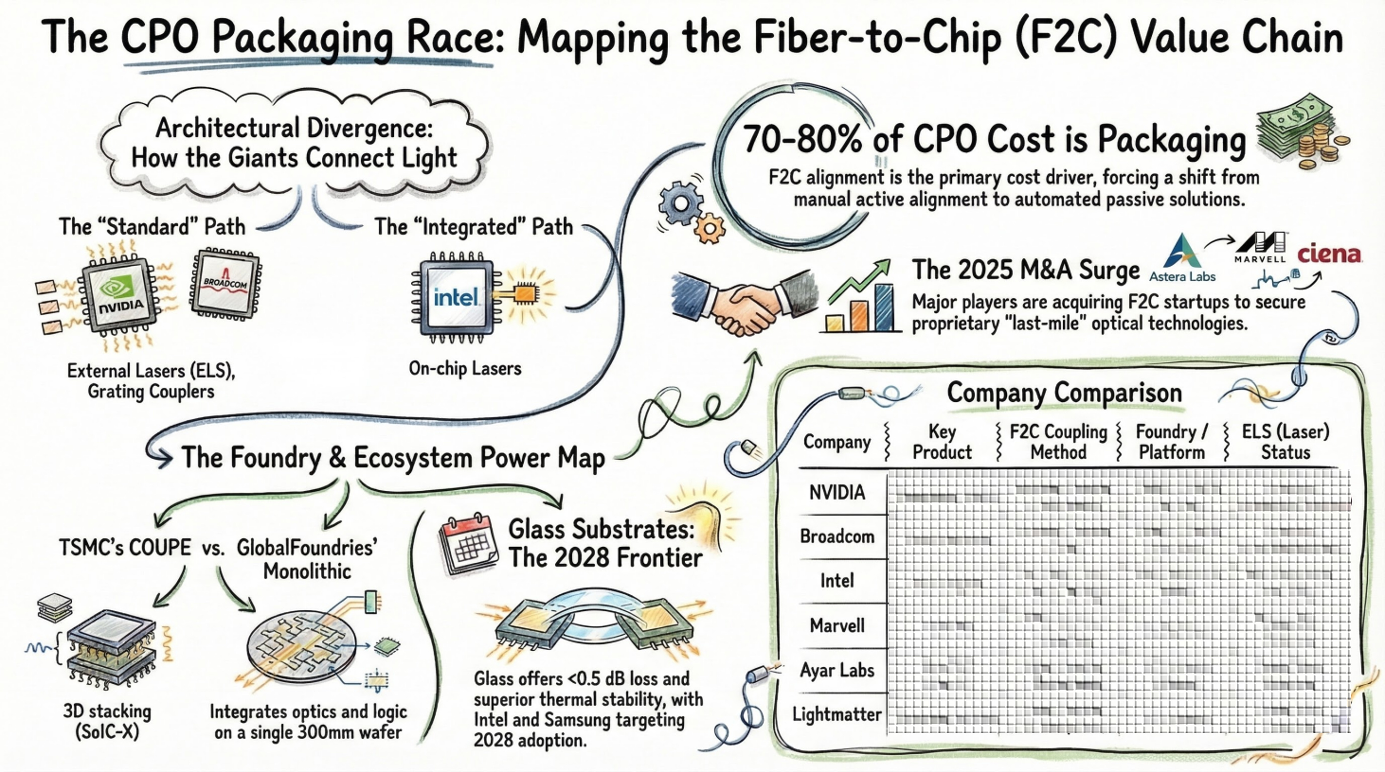
9. CPO Architecture by Product: Who Chose Which F2C Approach?
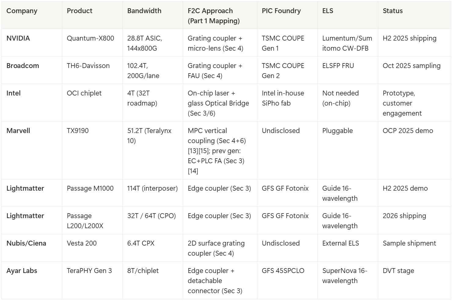
Let’s see how the coupling techniques from Part 1 are actually showing up in real products. NVIDIA, Broadcom, Intel, and Marvell are shipping or demoing CPO switches. Lightmatter and Ayar Labs are pursuing optical I/O chiplets and interposers. Nubis (now Ciena) is doing 2D surface coupling. Xscape Photonics is tackling on-chip multi-wavelength lasers. That’s at least eight competing approaches to F2C.
NVIDIA Quantum-X800 / Spectrum-X Photonics
NVIDIA unveiled two silicon photonics CPO switches at GTC 2025 [1][2].
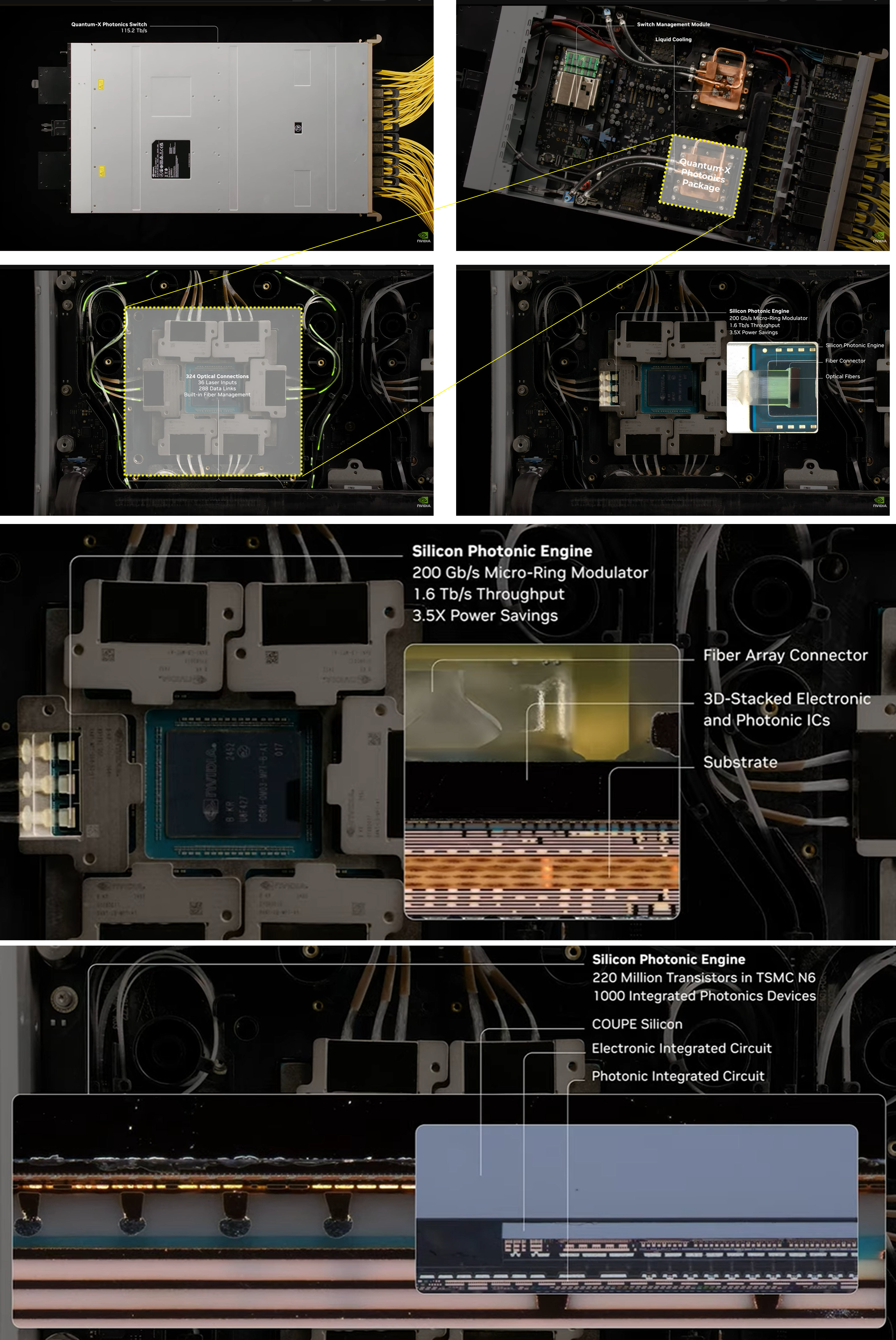
Quantum-X800 is the InfiniBand platform, built around a 28.8 Tbps ASIC (107 billion transistors, TSMC 4N) surrounded by six optical sub-assemblies. Each sub-assembly carries three engines, for a total of 18 x 1.6T silicon photonics engines [3]. Each engine takes CW-DFB laser light from an ELS (External Light Source) and modulates it with 200 Gbps micro-ring modulators (MRM) [2][3].
The F2C story here centers on TSMC’s COUPE (Compact Universal Photonic Engine) platform. A PIC (65nm process) and EIC (6nm process) are 3D-stacked via SoIC-X, with vertical O-band grating couplers on the surface coupling to fiber through micro-lens arrays [2][4]. COUPE reports fiber-array coupling loss at the 0.3 dB level [4]. The Quantum-X800 uses COUPE Gen 1 (1.6 Tbps engine for OSFP), with initial shipments in late 2025 and volume ramp in 2026 [4][5]. This design leans heavily on the grating coupler advantages from Part 1 Section 4: 2D arrays anywhere on the chip surface, plus wafer-scale passive alignment.
Per NVIDIA’s official blog, the F2C supply chain includes TSMC (COUPE process), SPIL (packaging), Lumentum/Sumitomo/Coherent (ELS assembly and optical alignment/test), Corning/Senko/Browave/TFC (connectors and fiber assemblies), and Foxconn/Fabrinet (system assembly) [2]. Quantum-X InfiniBand ships H2 2025. Spectrum-X Ethernet (SN6810: 102.4 Tbps) ships 2026 [1][2].
Broadcom Bailly / Davisson
Broadcom has the most generational depth in CPO. Three generations shipped so far [6][7]. Gen 1 TH4-Humboldt (2021) was a learning platform: Tomahawk 4 at 25.6 Tbps, a hybrid mix of optical (4x 3.2T SCIP engines) and electrical (32x QSFP112) channels. Tencent ran the initial deployment.
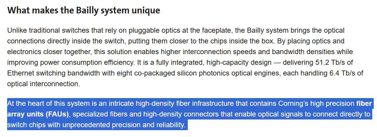
Gen 2 TH5-Bailly was the industry’s first volume-production 51.2 Tbps CPO Ethernet switch. Eight 6.4T SiPho optical engines, and Meta validated it with millions of hours of field testing [7]. The F2C structure uses TSMC COUPE, same as NVIDIA, and Corning supplies the Photonic Grade FAU, specialized fibers (including CPO FlexConnect), and high-density connectors [8]. Corning positions alignment precision to PIC waveguides as their core differentiator [8].
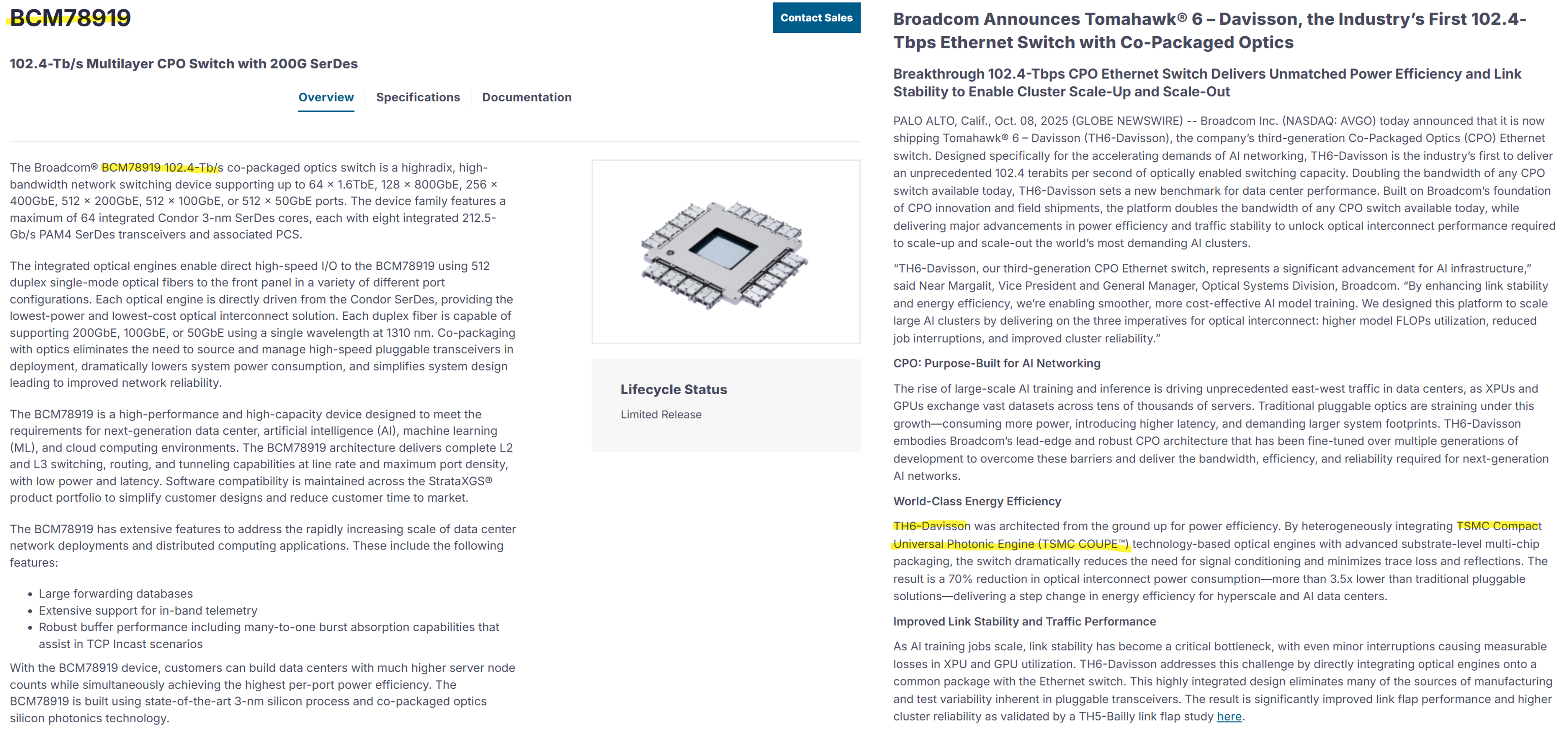
Gen 3 TH6-Davisson (BCM78919) started shipping in October 2025. 102.4 Tbps, 200G/lane, doubling Bailly’s bandwidth [6][7]. Sixteen 6.4T Davisson DR optical engines on TSMC COUPE Gen 2 [6]. Package size grew to roughly 120mm x 120mm, and the laser module now uses the ELSFP form factor, making it field-replaceable [6][7]. This tracks closely with OIF (Optical Internetworking Forum) standardization efforts, which suggests Broadcom is aiming for interoperability rather than a closed ecosystem. Power is 3.5W per 800G port, more than 70% lower than pluggable optical interconnects [6]. A Gen 4 CPO (400G/lane) is already in development [6].
Intel OCI (Optical Compute Interconnect)
Intel’s F2C philosophy is fundamentally different from the rest of the CPO field. The key differentiator: no External Light Source (ELS) needed [9][10].
Intel’s OCI chiplet integrates DWDM laser arrays and semiconductor optical amplifiers (SOA) directly on-chip in a single SiPho PIC [9]. Instead of pulling laser light from an external module (the NVIDIA/Broadcom COUPE + ELS approach), Intel has internalized this with over 25 years of hybrid laser-on-wafer technology. The production track record: 8 million+ PICs shipped, 32 million+ on-chip lasers [9].
The Gen 1 OCI chiplet demonstrated at OFC 2024 delivers 4 Tbps bidirectional, PCIe Gen5 compatible, pushing 8-wavelength DWDM (200 GHz spacing) across 8 fiber pairs for 64 channels at 32 Gbps each [9]. Power consumption is 5 pJ/bit, 3x more efficient than pluggables (~15 pJ/bit), with a roadmap to 32 Tbps [9]. Like Ayar Labs’ UCIe chiplet, it targets universal co-packaging with any SoC (CPU, GPU, IPU).
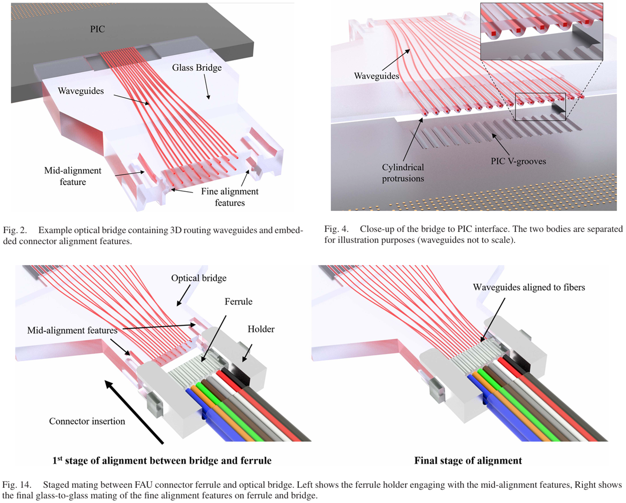
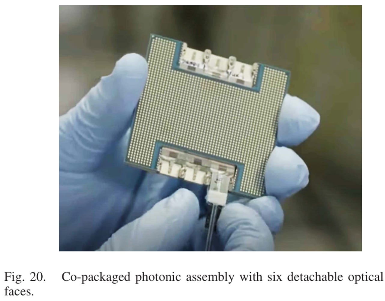
From an F2C standpoint, Intel’s other big contribution is the Detachable Optical Chiplet Connector [10]. Published by Psaila et al. in JLT (2023), this uses a glass-integrated waveguide Optical Bridge to connect the PIC to fibers in a detachable configuration [10]. Insertion loss is under 0.4 dB, repeatability is within +/-0.05 dB across multiple mate/demate cycles, and it survives 260C solder reflow [10]. That last point matters a lot. It means you can run the full electronic packaging flow (reflow included), then attach the optical connector afterward, and everything still works. This is a fundamental workaround for the epoxy shrinkage problem we’ll cover in Section 13.
Intel also holds 600+ patents on glass substrates [11], making it a core IP holder for the glass-based CPO story in Section 12.
Marvell TX9190
Marvell demoed the TX9190 liquid-cooled CPO switch at OCP Global Summit 2025, jointly with Jabil [12][13]. The base ASIC is the Teralynx 10 (51.2 Tbps), the same die already in volume production for copper switches [12]. The TX9190 is the CPO version with co-packaged optical engines.
Marvell’s F2C approach has evolved across generations. In Nagarajan et al.’s 2023 IEEE JSTQE paper, the architecture heterogeneously integrates DRV/TIA/DFB lasers on a SiPho interposer in 2.5D, then edge-couples a PLC (Planar Lightwave Circuit) fiber array assembly. Coupling loss was under 1 dB [14]. But the TX9190 (OCP 2025) uses SENKO’s Metallic PIC Coupler (MPC) [13]. The MPC is a microlens-based detachable connector that couples vertically to the PIC surface, the same family as the SSC + trench + microlens architecture that SENKO and GFS announced at ECOC 2025 [15]. In other words, Marvell appears to have transitioned from PLC FA (edge) to MPC (vertical coupling). Each XPU connects to four 6.4T light engines, each engine carrying two 36-fiber MPCs [13]. Per tray: 4 XPU × 4 engines × 2 MPC × 36 fibers = 1,152 fibers. Marvell’s blog quotes over 36,000 fibers at the rack scale [13]. Working backward, that corresponds to roughly 32 trays (36,000 / 1,152 ≈ 31.25).
Nubis Communications (now Ciena)
Nubis was founded by Peter Winzer in 2020 and acquired by Ciena for $270M in 2025 [16].
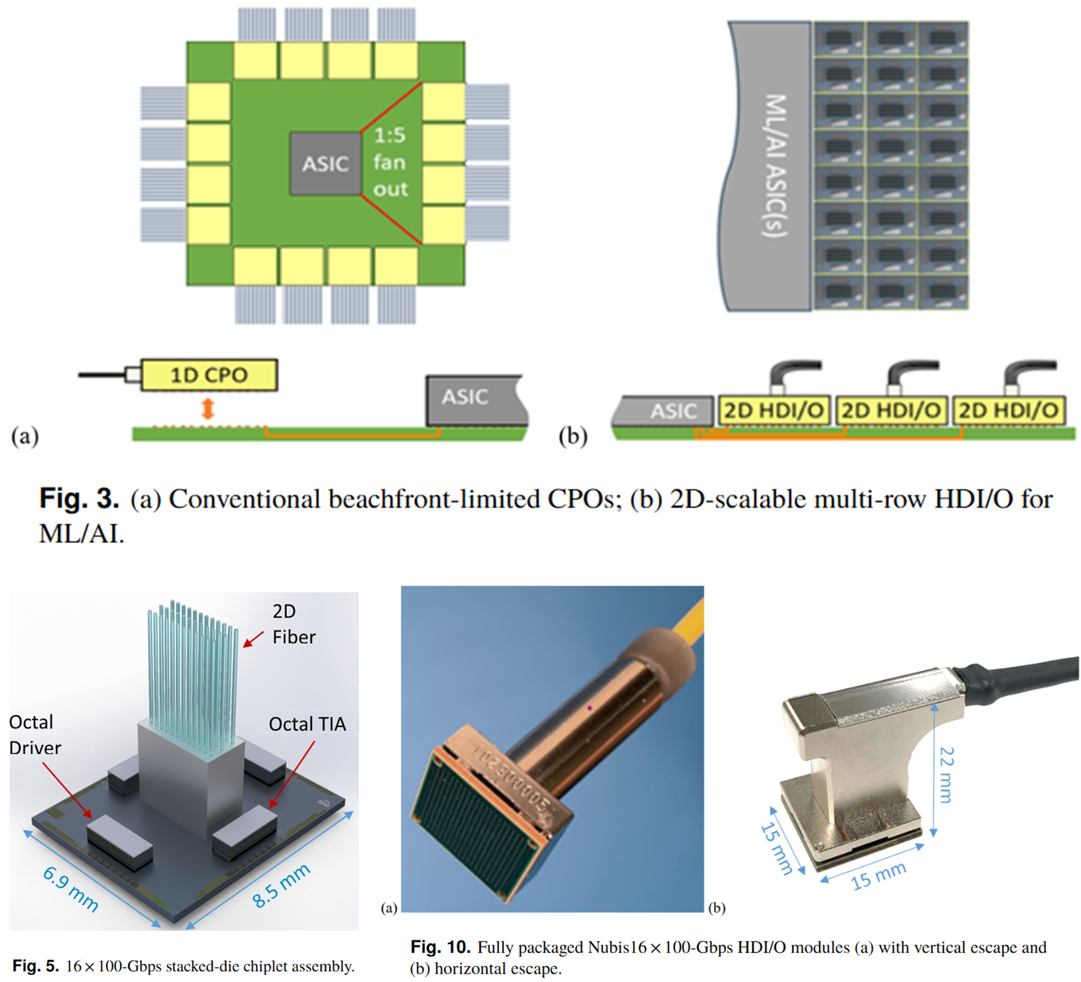
The F2C differentiator is 2D surface coupling [17]. This fundamentally sidesteps the “beachfront bottleneck” from Part 1 Section 3.3. Thirty-six fibers (32 data + 4 ELS) sit in a 3x12 2D array and couple through grating couplers on the chip surface [17]. The optical engine itself measures 5mm x 7.5mm, housed on a 15mm x 15mm XT1600 module substrate [17]. Full-duplex 1.6 Tbps at under 4 pJ/bit [16][17].
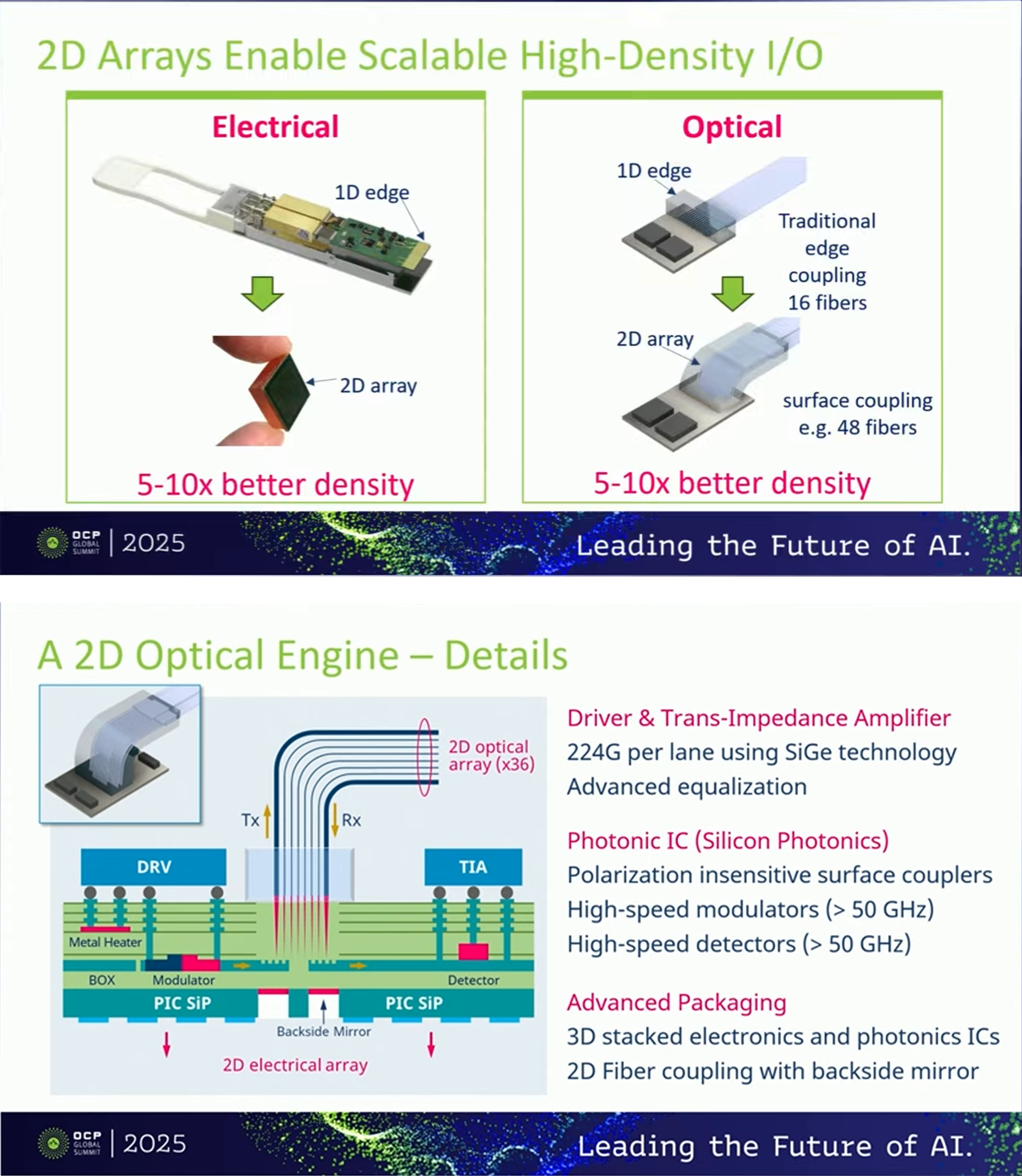
A 2025 Optics Express paper published the measured performance data [18]. The SDA (Silicon Die Assembly) measures 6.9mm x 8.5mm, running 16 x 106.25 Gbps full-duplex linear-drive, achieving a chiplet edge I/O density of 246 Gbps/mm (SDA edge basis, scalable to Tbps/mm with 2D arraying), operates at up to 85C case temperature without significant degradation, reaches 2 km on standard SMF, and bridges 58 dB of total electrical link loss between TX and RX SerDes using built-in analog equalization [18]. Achieving this without a DSP retimer is the key point. Nubis/Ciena partnered with Samtec to announce the 200G/lane Vesta 200 6.4T CPX (copper and optics interchangeable in the same footprint) [19].
Lightmatter Passage
Lightmatter differentiates with a 3D photonic interposer approach [20][21]. Passage M1000 is a multi-reticle active photonic interposer exceeding 4,000mm², delivering 114 Tbps total optical bandwidth [20]. It’s made of 8 tiles with reconfigurable waveguide mesh and optical circuit switching (OCS) built in [20][21].
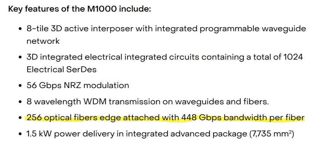
From an F2C perspective, M1000 completely eliminates the beachfront bottleneck. It provides electro-optical I/O from anywhere on the surface to die complexes stacked above, with 256 fibers edge-attached [20]. Modulation uses micro-ring modulators with 16-wavelength WDM [21]. Foundry is GFS GF Fotonix, packaging by Amkor [20]. The ELS is Lightmatter’s in-house Guide light engine (16 wavelengths) [20].
Passage L200 is the 3D CPO chiplet: 32 Tbps (L200) / 64 Tbps (L200X), with UCIe interface support [21]. Shipping expected in 2026 [21].
Ayar Labs
Ayar Labs takes the “optical I/O chiplet” approach. Not a switch-specific CPO, but a universal optical chiplet [22][23].
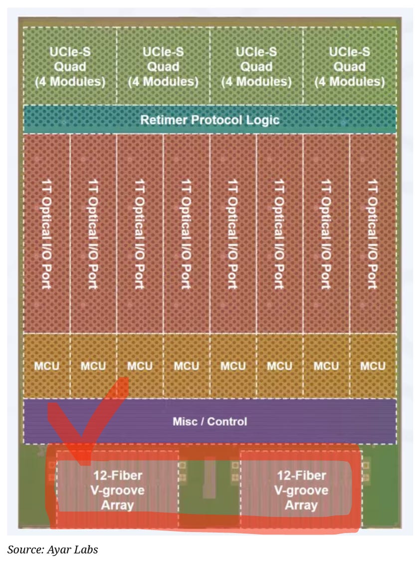
The Gen 3 TeraPHY chiplet is fabricated on GFS 45SPCLO 45nm SiPho, delivering 8 Tbps bidirectional [22][23]. It’s the industry’s first UCIe (Universal Chiplet Interconnect Express) optical chiplet, protocol-agnostic across CXL, NVLink, UALink, and Ethernet [22]. Modulation is MRM with 16-wavelength WDM, using the SuperNova DFB 16-wavelength ELS [22]. F2C is edge coupler + detachable optical connector, coupling at the PIC facet with post-assembly detachability [23]. At TSMC OIP 2025, Alchip and Ayar Labs demoed a prototype integrating 2 accelerators + 8 TeraPHY chiplets + 8 HBM stacks, reaching 100+ Tbps scale-up bandwidth per accelerator [24].
Xscape Photonics: Multi-Wavelength Comb Laser
Xscape Photonics is not an F2C play per se, but it affects CPO light source architecture, so it’s worth a brief mention. Backed by NVIDIA and Cisco, this U.S. startup built an on-chip optically-pumped multi-wavelength laser (ChromX) on Tower’s PH18 platform [25]. It supports CWDM/DWDM grids and claims scalability up to 128 wavelengths [25]. In a DWDM CPO world where you want terabits per fiber, reducing the connector and fiber count through wavelength multiplication is a real benefit.
Key takeaway: NVIDIA and Broadcom are converging on TSMC COUPE (grating coupler + micro-lens). Intel built a standalone path with on-chip lasers + glass optical bridges, eliminating the ELS entirely. Marvell is transitioning to SENKO MPC (vertical coupling), Lightmatter and Ayar Labs take edge-coupler chiplets on GFS, and Nubis/Ciena pushes 2D surface coupling for density.
10. Foundry F2C Strategies: Baking Coupling into the Process
Section 9 covered F2C at the product level. Now let’s go one layer deeper: how foundries are embedding F2C solutions into their process flows and PDKs. The question is not just “who makes SiPho,” but “how does the foundry design coupling loss and alignment tolerance at the process level?”
