
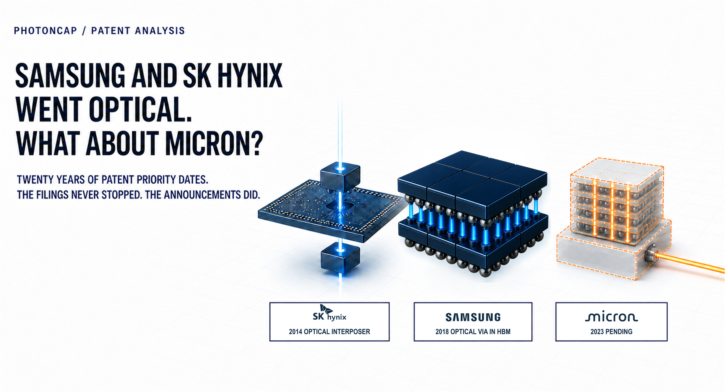
SK hynix announced on August 20 that its co-packaged optics roadmap paper had run in Nature Electronics[1]. CPO puts the optical chip that moves signals as light inside the same package as the compute chip.
I opened the paper right away and followed the twelve authors’ backgrounds and where the company had put money before that, which I wrote up in One Interconnect Company, All Three Memory Makers on the Cap Table: Fifteen Months of SK hynix’s CPO Track. Something stayed with me after I filed that one.
The paper is a review. It reads less like a company product roadmap and more like a summary of where the field has gotten to, with tables of energy and bandwidth per integration method and a list of problems still open.
The newsroom post had a different flavor. There the company put its own name behind a bigger claim, that memory would be bound into a single pool to get past the memory wall[1]. The paper surveys, the announcement points.
So I got curious. Is this only SK hynix’s direction?
Samsung is already out in public. Its foundry declared entry into silicon photonics in March and published a schedule. That leaves Micron, which has no roadmap, no paper, and no press release on optics from the last ten years.
So I went to the patents. And one filing came back with a February 2023 priority date that is still under examination. The title is optical signaling for stacked memory device architectures. Memory dies stacked up, with light running between them.
Something the company has never said out loud is sitting at the patent office right now.
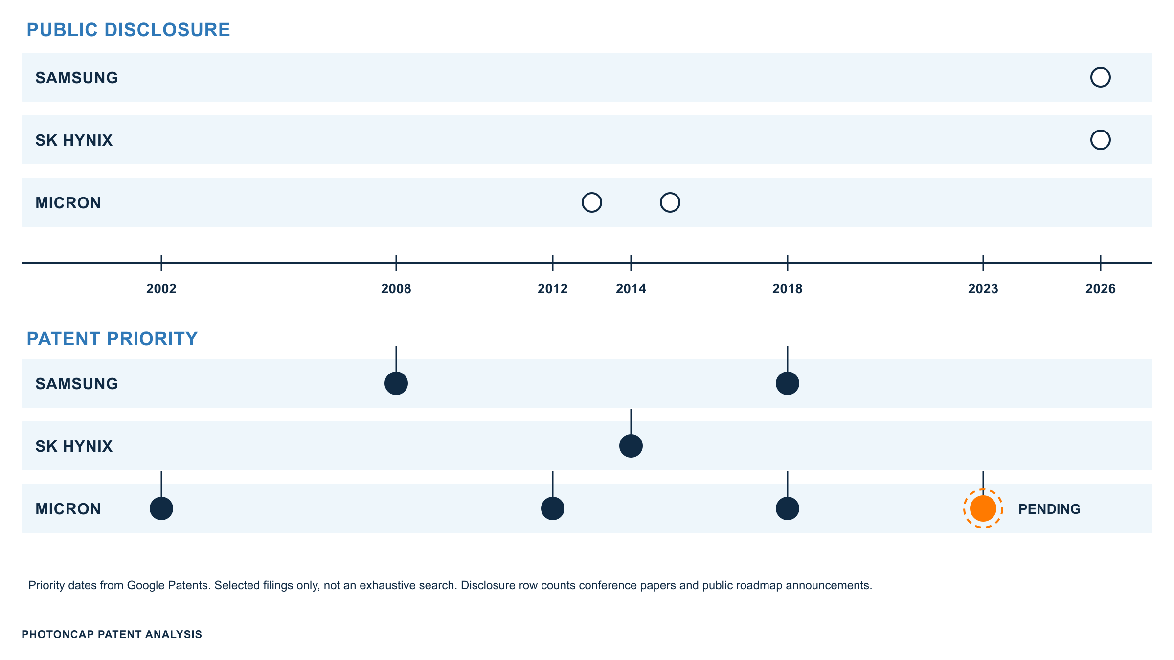
Three memory makers on two axes, public disclosure above and patent priority below
TL;DR
SK hynix’s Nature paper reads mostly as a review, but the newsroom post put the company’s name behind memory pooling as the way past the bandwidth bottleneck
Samsung already stands in the same place as a foundry product. It laid down a PDK at OFC and published a turnkey schedule
Micron has no public optical roadmap from the last ten years, so I went through patents and job postings instead
Binding memory with light is an idea more than twenty years old. Micron filed in 2002 and Samsung in 2008
Narrowed to the silicon photonics package family, Micron has a 2023 priority filing that is still under examination
Lined up by priority date, filings recur across several generations from 2002 to 2023. What clearly stopped was the public announcements
Contents
Why This Comes Up Now
Samsung Is Already Standing There
No Announcements, So Open the Patent File
The Role Micron Is Hiring For
Ten Billion Dollars and August 27
Four Layers That Are Easy to Miss
Where This Goes
References
1. Why This Comes Up Now
Memory bandwidth has come up several times in this series. The routes to more bandwidth and the paths for moving capacity outside the package are laid out in Three Routes Around the Memory Wall: Qualcomm’s Stack, Nvidia’s 3 Bits, and What Remains.
The short version. Putting memory right beside the GPU made it fast and also made capacity hard to grow. Stacking more layers is getting expensive in heat and yield. So the remaining path is to move memory outside the package and connect it through a channel.
Right now that channel is copper. CXL is the one. It works, though round trip latency runs somewhere around double what local memory costs. The number moves with the device, the number of switch hops, and the memory media, so pinning it to one figure is hard. Either way it is slower, which means software has to keep deciding what sits near and what sits far.
The targets in the SK hynix paper are worth noticing here. More than 100Tb/s per node, under 1 picojoule per bit, and chip to chip latency below 10 nanoseconds[1][2]. That last number is aggressive. It is a target for the chip to chip optical link though, not for end to end memory access, since controller, protocol, queuing, and coherence costs stack on top of it. Even so, a link at that level would make tier management much lighter than it is today.
The paper says as much itself. It leaves an optical memory interface that keeps coherence while lowering latency on the open problems list[1]. The picture got drawn and the method got assigned as homework.
Here is where it splits, why a memory company would look at this directly. Turning the channel optical used to belong to the networking companies and the foundries, since CPO started by putting an optical engine beside a switch. But when the thing at the far end of the channel becomes memory, the situation changes. The optical chip has to come inside the memory package, and the company that designs, assembles, and tests that package is the memory company. It stops being somebody else’s problem.
2. Samsung Is Already Standing There
I mapped Samsung once in July. In TSMC Is Ahead in CPO. Samsung Is Putting a Third Chip Next to HBM I laid out who holds which of the chips that go on the interposer, and Samsung was the only one holding memory, logic, and the optical chip together.
It has moved further since. At OFC 2026 on March 17 the foundry division formally declared entry into silicon photonics and said its PDK was complete[3]. A PDK is the toolkit customers design with. Its arrival means customers have a base to start design and tapeout from. It does not mean production yield and process qualification are finished. The kit reportedly carries more than forty device models with a verification flow, on a 300mm process[3].
[OFC 2026] Part 1 of 5: 300mm SiPh Foundry: Who Is Actually Ready?
![[OFC 2026] Part 1 of 5: 300mm SiPh Foundry: Who Is Actually Ready?](https://substackcdn.com/image/fetch/$s_!zc4V!,w_1300,h_650,c_fill,f_webp,q_auto:good,fl_progressive:steep,g_auto/https%3A%2F%2Fsubstack-post-media.s3.amazonaws.com%2Fpublic%2Fimages%2F22cba2f2-fc29-43bd-b592-166665f23944_2949x1557.png)
Two Ways to Read a Conference Paper
Why the PDK matters is that optical devices diverge from simulation more than electrical ones do. A modulator that behaves in the schematic often comes back strange on the actual wafer. The PDK is the foundry’s attempt to shrink that gap before handing it over, and without one you cannot build a repeatable standard design flow. That is also why Samsung bothered to mention that free carrier absorption and self heating went into the models[3].
The schedule went public too. Thermocompression bonded optical engines in 2027, turnkey CPO service in 2029[4].
That is the visible picture. Samsung tells you because Samsung has to sell. A foundry only has a business when customers knock, and that means saying where you are, repeatedly.
So what about Micron?
I searched by silicon photonics, optical I/O, CPO, and conference presentations, and nothing recent comes back. Recent OFC and ECTC programs carry no Micron optical talk, and no optical interconnect startup investment shows up either. As far as I can find, the company has issued no press release on the subject at all.
When there are no announcements you look somewhere else. I opened the patent file and the job postings.
What follows is that record. Line the three companies up by priority date and the order comes out different from the market’s impression, and on Micron’s side one filing is still waiting on examination. The qualifications on a currently open job posting carry a word the company has never put in a press release. The dates on the Boise lab announcement and the SK hynix Indiana groundbreaking sitting a week apart, and Micron’s continued absence from the US government optical programs, both come up later.
The last part is the value chain. Everybody already says packaging benefits when memory gets pooled, so instead I pulled four layers that rarely get named. They are process steps you pass through whichever way the architecture goes.
