
Abstract
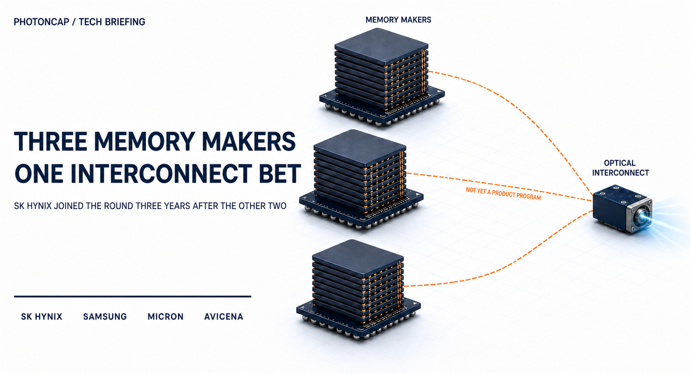
On August 20 SK hynix used its own newsroom to announce that a co-packaged optics roadmap paper had been published in Nature Electronics. CPO means putting the optical transceiver inside the same package as the processor. The company’s post leans on two things: Seunghoon Hong, its AI Infra team lead, served as a corresponding author, and the work goes beyond HBM innovation to a system-level blueprint. I read the post, opened the 15-page paper next to it, and then walked through the public record of all twelve authors one by one. That is when I found out this track did not start with the paper. The company post has not one line about the step before it. I treat this announcement as a positioning signal rather than a CPO product schedule. What holds up is that the technology choice was already marked in money, with all three memory makers leaving that mark side by side.
Contents
The company published this itself
The wall the paper draws
The table the post left out
Twelve authors and where they come from (Paywall)
Where the track actually starts
The same cap table
The distance still left
How far I take this
1. The company published this itself
Here is the headline that went up on the SK hynix newsroom dated August 20.
“SK hynix’s technology roadmap for co-packaged optics features in ‘Nature Electronics,’ as AI competition shifts from chips to systems” [1]

SK hynix newsroom post
The paper is “Co-packaged optics for high-performance computing and artificial intelligence,” the journal is Nature Electronics, and the format is a Review article. The front page is stamped submitted November 18, 2025 and accepted July 8, 2026 [2].
The company names two corresponding authors. Seunghoon Hong, team lead at AI Infra, SK hynix, and Professor Kyusang Lee of the Department of Electrical and Computer Engineering at the University of Virginia [1]. The collaborating institutions are listed as UIUC, NTU, MIT and Yonsei.
Look at the paper itself and there are twelve authors. Nature titles attach a contact e-mail only to corresponding authors, and the bottom of the first page carries six e-mail lines, one of them on the sk.com domain [2]. So the company took those six and introduced two of them as the lead corresponding authors.
AI Infra is an organization SK hynix set up in January 2024. By the company’s own newsroom description it groups global sales and marketing, the HBM business, and Memory System Research, which does pathfinding beyond HBM [3].
The newsroom even added a footnote defining what a corresponding author is. Principal authors who oversee and take responsibility for the whole process, from planning through submission, peer review response, and post-publication questions [1]. The fact that the company bothered to footnote that phrase tells you where the weight of this announcement sits.


The company did not leave this in an internal research news column either. The official X account pushed the same content on the afternoon of August 19 local time, with the hashtags #SKhynix #CPO #AIInfrastructure [4]. The Korean newsroom date reads August 20 because that is Korea time, so the global channel started the day before.
The X wording carries one more edit, though.
“Published in Nature Electronics, a new paper from @SKhynix and University of Virginia researchers explores how CPO can overcome the ‘bandwidth wall’ through optical connectivity.” [4]
SK hynix and University of Virginia researchers is all that survives in that sentence. The Korean newsroom lists UIUC, NTU, MIT and Yonsei too [1], and they are gone from the global channel. By author count the MIT and UIUC share is not small.
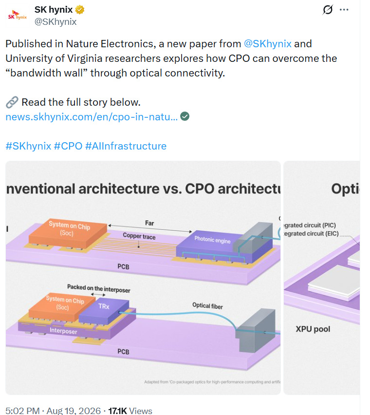
A memory company taking part in an optical interconnect review is not new by itself. A company turning that into an external message is a different thing. And the one partner name left standing in that message is the University of Virginia, which comes back later.
2. The wall the paper draws
The term the paper’s own text uses for this bottleneck is bandwidth wall. Memory wall shows up once, in a reference title. Here are the scaling numbers behind it. Every two years compute throughput went up 3x, DRAM bandwidth 1.6x, and interconnect bandwidth 1.4x, while on the same axis AI model training compute jumped 8.8x [2].
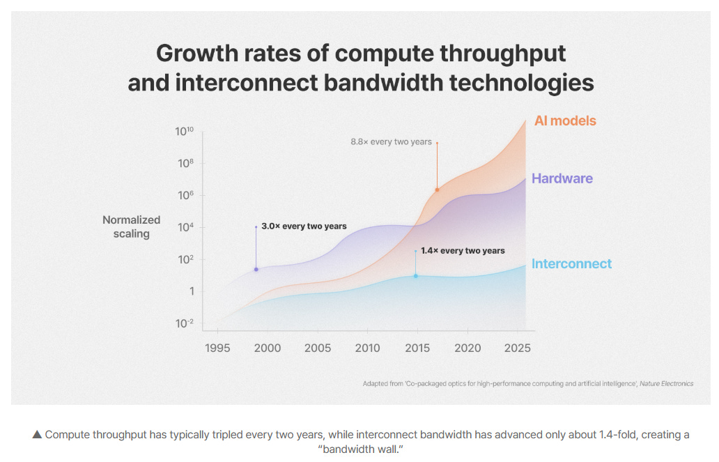
Newsroom scaling graphic, 3x compute against 1.4x interconnect
The company post quotes only two of those, the 3x and the 1.4x [1]. The paper has DRAM bandwidth at 1.6x sitting in the same figure. A memory company issuing a release with the DRAM curve dropped out is a curious edit.
So compute moves 3x while the pipe that carries the data moves 1.4x. The gap bites hardest at the boundary between memory and logic. Here is the paper’s own sentence.
“the gains are confined to intra-package communication; once data goes beyond the memory-logic boundary, electrical interconnects ... incur resistive and capacitive losses that greatly increase with frequency and distance” [2]
What HBM gained holds only inside the package, and the moment data crosses the memory-logic boundary the losses in copper take over again. You can stack DRAM dies with TSVs, which are vias drilled vertically through the chip to make the connections, and pull multiple terabits per second out of them, and that gain still will not follow the data out of the package.
This series has been over that diagnosis several times. Once in Three Routes Around the Memory Wall: Qualcomm’s Stack, Nvidia’s 3 Bits, and What Remains, which laid out three ways of raising memory bandwidth, and once on the optical memory fabric side in The More Anthropic Buys Micron HBM, the Faster Optical Memory Pooling Arrives. The diagnosis has been around for a while. A memory company putting its name on that chart and then issuing a release about it is the part that changed.
3. The table the post left out
The company post summarizes the paper’s technical targets in three lines. More than 100 Tb/s of bandwidth per node, energy below 1 pJ per bit, chip-to-chip latency under 10 ns [1]. The same numbers are in the paper [2].
There is one more table in the paper that the post did not carry over. Table 2, titled representative industrial CPO and optical I/O platforms in the original. It mixes shipped products, demonstrated prototypes and some projected figures, so not everything in it is in production. Broadcom Bailly and Davisson, NVIDIA Quantum-X Photonics, Intel OCI, Ayar Labs TeraPHY, Lightmatter Passage M1000, Celestial AI Photonic Fabric, Ranovus, Avicena, Microsoft MOSAIC. Ten rows, nine companies [2].
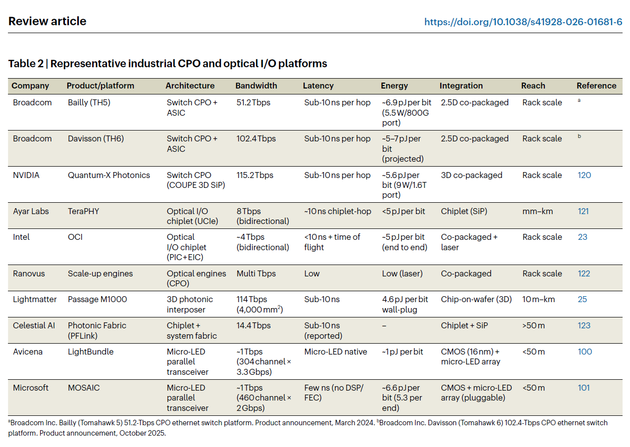
paper Table 2, industrial CPO and optical I/O platform list
Switch companies, accelerator companies and optical I/O startups are all in there, and the memory makers are the ones missing from the list.
This gap is something I already mapped once in July. In TSMC Is Ahead in CPO. Samsung Is Putting a Third Chip Next to HBM I mapped who holds each of the three chips that go on the interposer, meaning HBM, logic and the PIC. Samsung was the only one holding all three, and SK hynix held memory while sending the logic base die outside. That piece sorted SK hynix’s routes into CPO into three. Packaging verticalization in Indiana and Cheongju, the memory-system CPO review at the 2025 Future Forum, and the CPO ecosystem on the public-project side.
I went back to the original on that Future Forum item. It was held September 11, 2025 at the Icheon campus, and the third agenda was a joint presentation by KAIST Professor Kyoungsik Yu and SK hynix Vice President Hoyoung Son [5]. The title reads like this.
“A future connected by light: CPO (Co-Packaged Optics) technology evolution and its ripple effects on the memory industry” (author translation from the Korean original) [5]

SK hynix Future Forum 2025 newsroom
Son’s title is worth a second look. He is head of Advanced PKG Development [5], which is a package development organization rather than strategy or planning. And the content, per the newsroom, was sharing a review of silicon photonics technology types, working through how to apply it inside and around the memory system, and setting out what preparation is needed across Architecture, Design, Device and Package [5].
That July piece also left a monitoring item at the end. Watch whether the memory-system CPO reviewed at the Future Forum turns into an actual R&D program or a partner disclosure. This announcement is the first answer to that item. An academic partner is disclosed, and a company employee put his name on it as a corresponding author. It is still not confirmation that an R&D program is running, so I am leaving that item half filled rather than closing it.
A later figure in the same paper puts a memory pool and an XPU pool facing each other across a single photonic interposer [2]. The company post ran that same concept diagram [1]. The side with no name in the table takes up half of the future architecture.
The word CXL never appears in this paper. I checked by searching the full text. UCIe shows up five times in the same document, NVLink and PCIe twice each. The die-to-die standards and the network standards are covered, and the current standard for memory pooling is the one that is missing.
The paper talks about pooling memory without touching the electrical pooling standard the industry actually uses today. The right reading is that the review’s scope sits on the optical architecture side. A missing word and a deliberate exclusion are different claims, and I will not push it that far. Readers should account for the gap either way.
That is as far as you get from putting the paper and the release side by side. Checking the public record of all twelve authors one at a time makes it fairly clear where this collaboration came from. And there was a step before it that appears nowhere in the company post. A trace of money that moved before the paper did.
