
TL;DR
Acquired in February, two papers in May. Authors who used celestial.ai addresses last year filed on the same subject this year from marvell.com. One word in the title changed, from Assembly Process to Demonstration.
The two papers filled different halves. Last year measured the path the light would travel and left assembly for later. This year completed the assembly and pushed the optical measurement back. Only the diagonal is filled in.
So one cell is left empty. An optical link measured on an assembled OMIB package. It appears in neither paper.
Photonic Fabric is really three pieces. Assembly has been demonstrated, the link has been measured but on a different test vehicle, and system performance is all simulation.
Meanwhile the product came out on August 4. No customer name and no sampling schedule are attached, and the 32 terabytes in the marketing copy is the number the paper lists as a simulation configuration.
I am very bullish on $MRVL and ‘Photonic Fabric’ idea and I still like this acquisition. What I think is that the place where the call gets settled is not the August 27 print but next year’s conferences.
Contents
The papers that changed affiliation
The layer this piece looks at
What beachfront means
What OMIB is
The mold and the dam
Hitting the same wall electrically
The halves they traded
Three pieces, three stages
The question with no answer yet
Absence is a signal too
But the product lineup is already out
What I asked in April
Closing
1. The Papers That Changed Affiliation
Marvell closed the Celestial AI acquisition on February 2 of this year [1]. As announced at the time of the deal, the structure was $3.25B, with up to $2.25B more in performance based stock on top [2].
Four months later, at the end of May, two papers went up at ECTC 2026. One is about an optical bridge called OMIB [3], and the other is about the whole Photonic Fabric architecture [4].
The interesting part is the author list. There is a paper from ECTC 2025 with almost the same title [5], and the key people overlap. Of the six authors on last year’s paper, five appear across this year’s two papers: Aggarwal, Pothukuchi, Sahni, Winterbottom, and Lazovsky, who founded Celestial AI. Last year the email domain was celestial.ai. This year it is marvell.com.
One word in the title changed as well. Assembly Process became Demonstration. Last year’s paper did demonstrate part of the process and the optical path. It left the full assembly for later, and this year is the report that finished it.
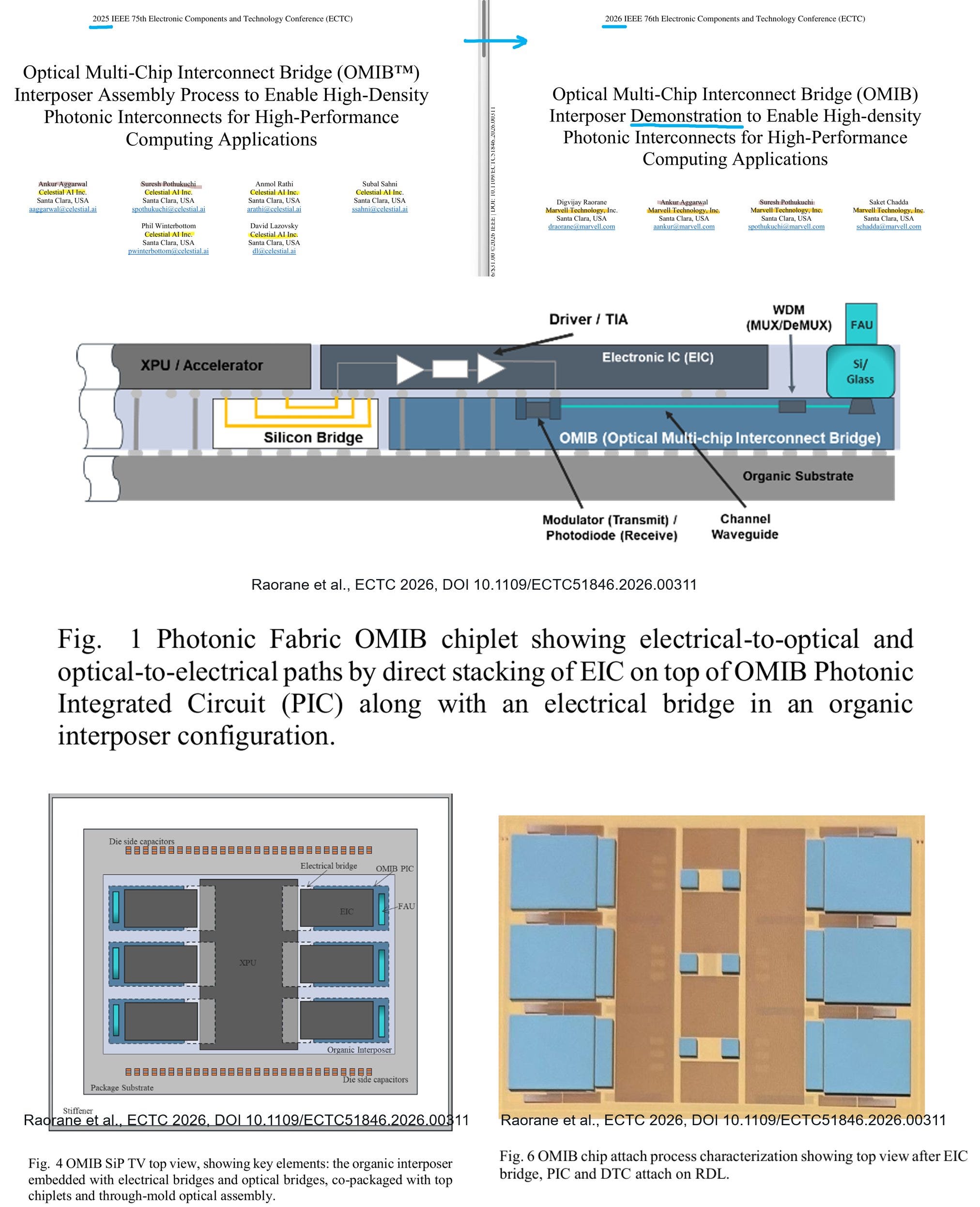
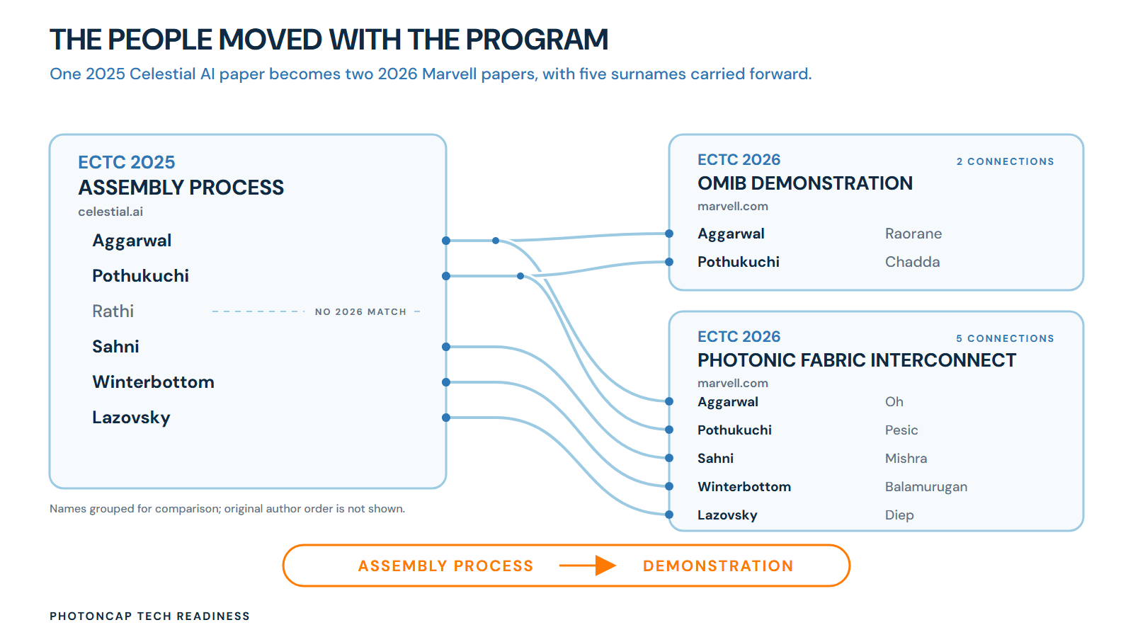
Author blocks compared, 2025 paper versus 2026 papers
If you want to know what the acquisition price bought, this is more honest than the press release. These are sentences an engineer wrote for a conference, not sentences a company picked for promotion.
2. The Layer This Piece Looks At
I want to place this piece first.
There is already a very careful piece tracking Marvell at the earnings and valuation layer. Damnang’s Marvell Part 3 is that piece, and it covers everything from the segment revenue bridge to the structure of the Google warrant. I read it closely.
On Photonic Fabric, that piece concludes as follows. It barely shows up in the income statement yet, only part of it is reflected in the valuation, and the confirmation point is when the first customer and the memory partner are disclosed.
That is an accurate read. On company guidance, the FY28 scale up optics outlook went from $150M to about double that, which is a rounding error next to the $16.5B revenue guide [6].
So this is a question about an option rather than about revenue. And the value of an option is set by how long it takes to be realized.
Damnang proposes learning that timing from disclosures. That works too, but there is also a way to read it one layer down first. The papers. This piece is about that lower layer.
So let me say up front that the clock for this piece is not the August 27 earnings release. This is not the kind of piece that turns out right or wrong on a number a few days from now. It measures where the gates are.
3. What Beachfront Means
Let me unpack one word before going into the technology.
The doors where data enters and leaves a chip are cut into the chip edge. But the length of a chip edge is fixed. Make the chip bigger and the area grows as the square, while the perimeter grows much more slowly than that.
Attaching optical modules beside the chip also ends up sharing that same edge. So if you want to keep raising bandwidth you need more doors, and there is nowhere to put them. This constraint is called beachfront. It means shoreline, and you can think of it as a question of how many ports you can build.
This is the wall the whole CPO camp is up against. I covered this subject in an earlier piece, The Optical Axis Alone Won’t Show It: Redrawing CPO Across Three Budgets, Energy, Heat, and Reach, splitting it into three budgets: energy, heat, and reach.
The answer OMIB proposes is this. Stop cutting the optical doors only into the edge, and put them directly under the place where the computing happens. The paper calls this a point of compute arrangement.
4. What OMIB Is
Start with the structure [3].
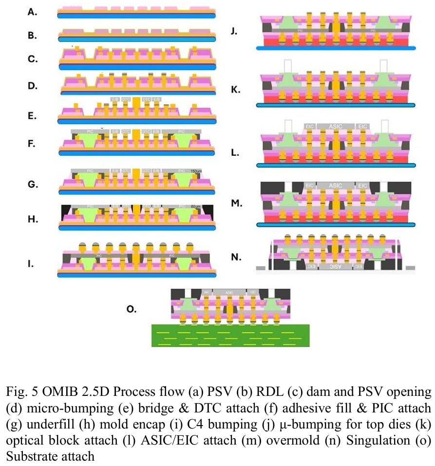
The photonic chip (PIC) is buried inside an organic interposer. The electronic chip (EIC) sits directly on top of it. The EIC and the XPU are joined by a silicon bridge.
The light does not exit sideways. It comes up out of a grating on the PIC surface, passes through a silicon or glass block that penetrates the mold, and meets a fiber bundle at the very top of the package.
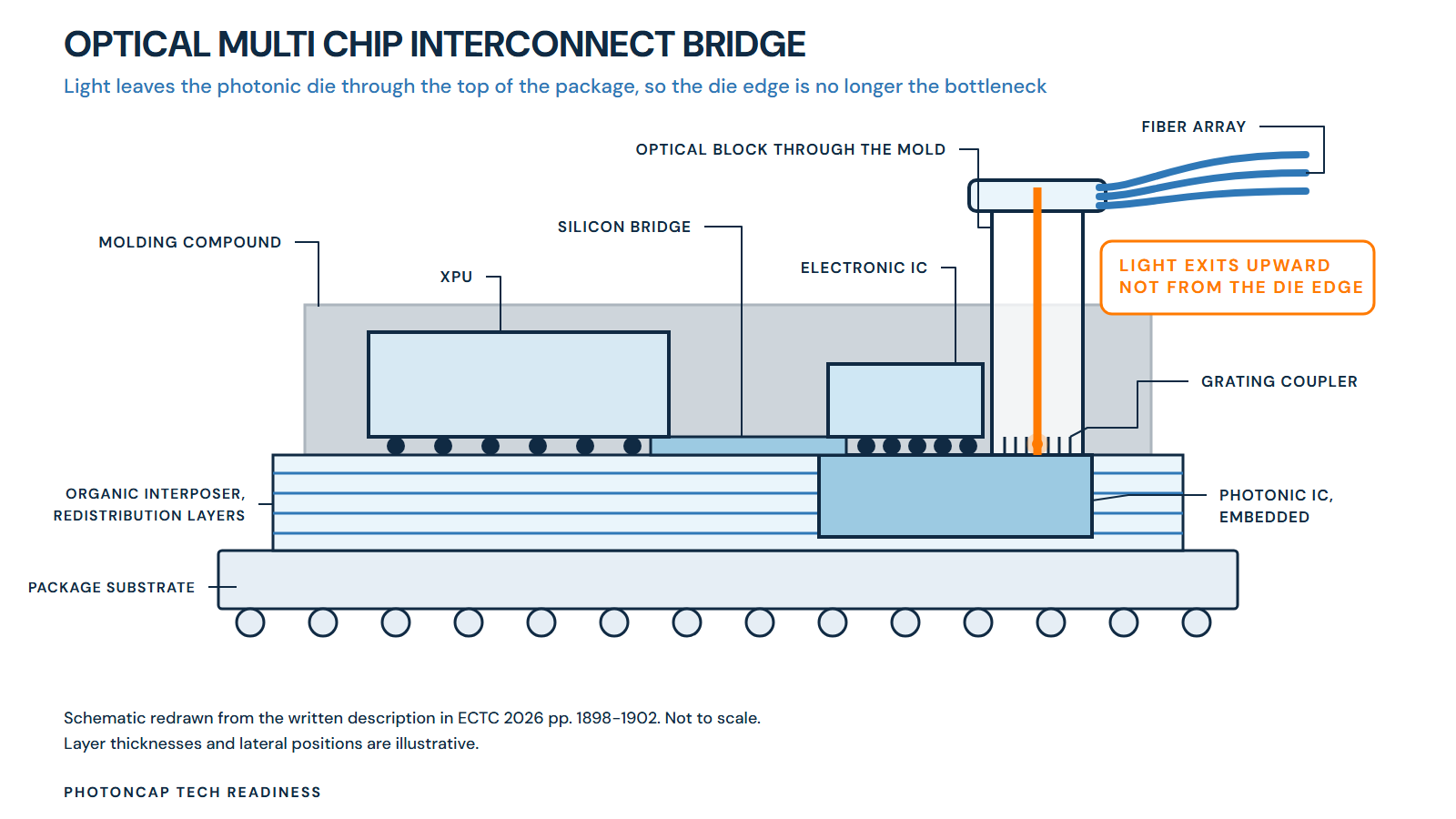
OMIB cross section and the optical path (schematic, redrawn from the paper’s description)
The phrase organic interposer may bother you here. It means this is not a silicon interposer. You coat a carrier with dielectric, plate copper, and repeat to build up wiring layers, and that is called RDL. The wiring is coarser than silicon and it warps more easily, but it is cheap and you can make it large.
And what the paper emphasizes is that this assembly is compatible with a standard 2.5D flow. The original wording is “amenable to scaling at OSATs,” which means it can run on an OSAT line. From here on this is my inference, but if so, it means optical packaging volume does not have to be tied to a particular foundry’s advanced packaging queue. The paper does not claim that far. It also did not show yield or capacity.
5. The Mold and the Dam
Where was the hardest spot in the assembly? This part was the most fun for me.
Semiconductor packages are black because after the dies are attached you pour black epoxy resin over everything and cure it. This is called molding, and the material is called EMC. You mix in a lot of silica powder to control thermal expansion, and you grind the top flat to build structure. It is the skeleton of a 2.5D assembly, so you cannot skip it.
But EMC is black, the silica scatters light, and the refractive index does not match the design either. If EMC covers a grating, that optical port is dead. The paper did not measure how much coverage causes how much degradation. It only reports that mold was kept out of the grating area.
So the requirements collide head on. The whole thing has to be molded, and the small windows over the gratings must never be touched by EMC.
The method Marvell used is a dam. They build walls of polyimide around the grating window. It is the same as setting formwork around one hole before pouring concrete. The inside of the window is filled with index matched optical adhesive.
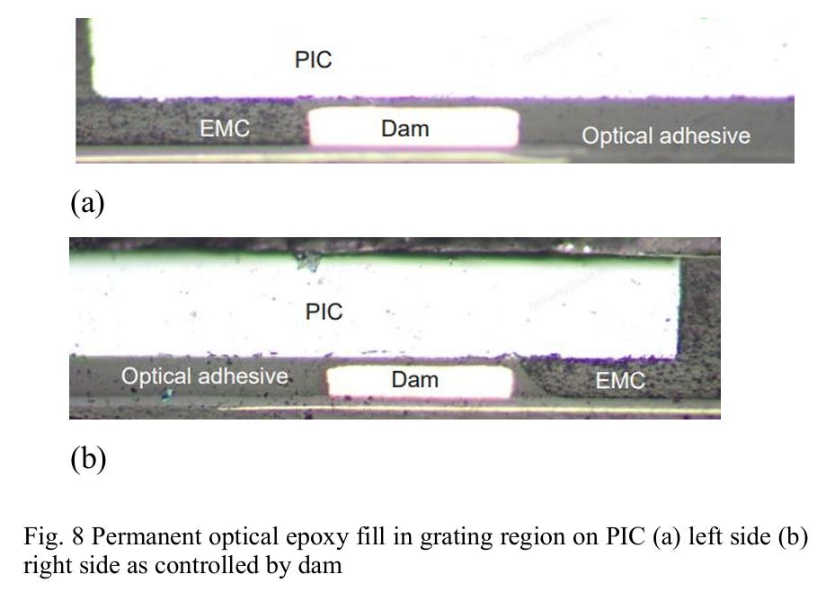
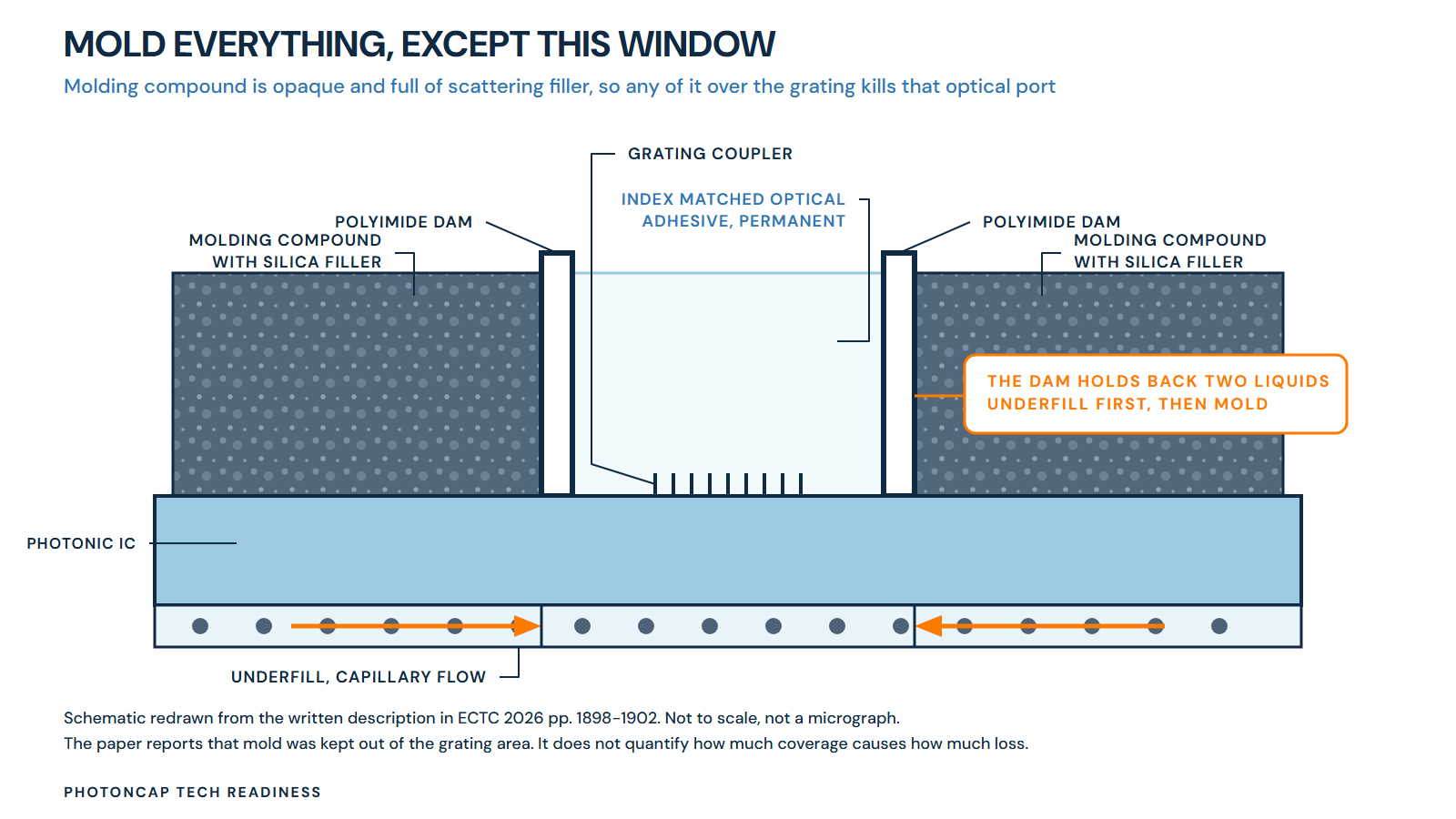
The dam holding back EMC, both walls of one window (schematic, redrawn from the paper’s description)
That cross section appears in a figure in the paper. The dark, grainy EMC stops dead at the white dam wall, and inside there is nothing but clean adhesive. They shot the left wall and the right wall of a single window separately to show that both held.
To add one thing about why this is hard, the first opponent the dam has to hold back is underfill, not EMC. Underfill is material you flow under the PIC on purpose to fill around the bumps, and it is not pushed by pressure. It works its way in by capillary action. The narrower the gap, the more strongly it is drawn in. Two liquids have to hold their own territory in the same gap.
And the dam sits under a die, so it is invisible during the process. If one spot leaks there is no obvious way to save that optical port, and the paper does not give repair options or a reject criterion.
6. Hitting the Same Wall Electrically
Optics is not the only way over the wall. The third paper Marvell put into the same conference is on the electrical side [7].
It is about custom HBM. They strip out the standard JEDEC PHY and put a dedicated interface on the logic base die of the HBM stack, and the numbers are fairly strong. Interposer channel length goes from 6.5 millimeters to 1.5 millimeters, and the area the HBM PHY was eating on the host chip shrinks by close to 60%.
Same 2µm design rules, same nine routing layers, and per lane speed becomes two and a half times. These figures are channel simulation results rather than measurements.
The EMIB-T paper Intel put into the same conference gives the opposite answer [8]. They keep the 6 millimeter channel and hold on with equalization. At 12 Gb/s the eye width lands right on the budget line without correction, and margin only appears once DFE is on. These are full channel simulation results as well.
It is interesting that two companies gave different answers to the same wall, but for the argument of this piece the point is this. Marvell is hitting this wall from the optical side and the electrical side at once. It is also a physical reason why content per socket keeps rising for custom silicon. If you can give a customer back area to spend on compute, they hand you more.
7. The Halves They Traded
Let me bring the story back to OMIB. That is what this year’s paper showed, so what has it not shown yet? Yes, as you have guessed, performance.
Put last year’s paper and this year’s paper side by side and they split like this.
Last year (2025) measured the optics. They polished the glass block with CMP down to roughly one nanometer surface roughness, and measured the peak wavelength and peak loss of gratings through that block on two wafers, comparing against a baseline [5]. But that was a test setup where a glass spacer sat on the gratings of a PIC test chip and a lensed fiber bundle received the light, and the paper itself wrote that the full assembly flow was left for future work.
This year (2026) completed that full assembly. They buried 24 dies in the interposer, molded, ground, flipped, placed the optical blocks, put the XPU on, and attached it to the substrate. The joint cross sections are the evidence [3]. But an important qualifier is attached here. This test vehicle was designed as a passive daisy chain structure. The XPU, the EIC, and the PIC are all test chips, and the optical side is a passive loopback. It was built to see whether the wiring connects and whether the assembly works, not as a working product. And the optical measurement section defers to a citation of last year’s paper and ends like this. Measurement on assembled units will come after reliability testing.
To put it together. Last year’s paper measured the path the light would travel and did not carry assembly to the end. This year’s paper carried assembly to the end and did not measure the light. What one paper filled, the other left empty, and what the other filled, the first left empty.
Only the diagonal is filled in. A paper with both cells filled, meaning an optical link measured on an assembled OMIB package, appears in neither of these two.
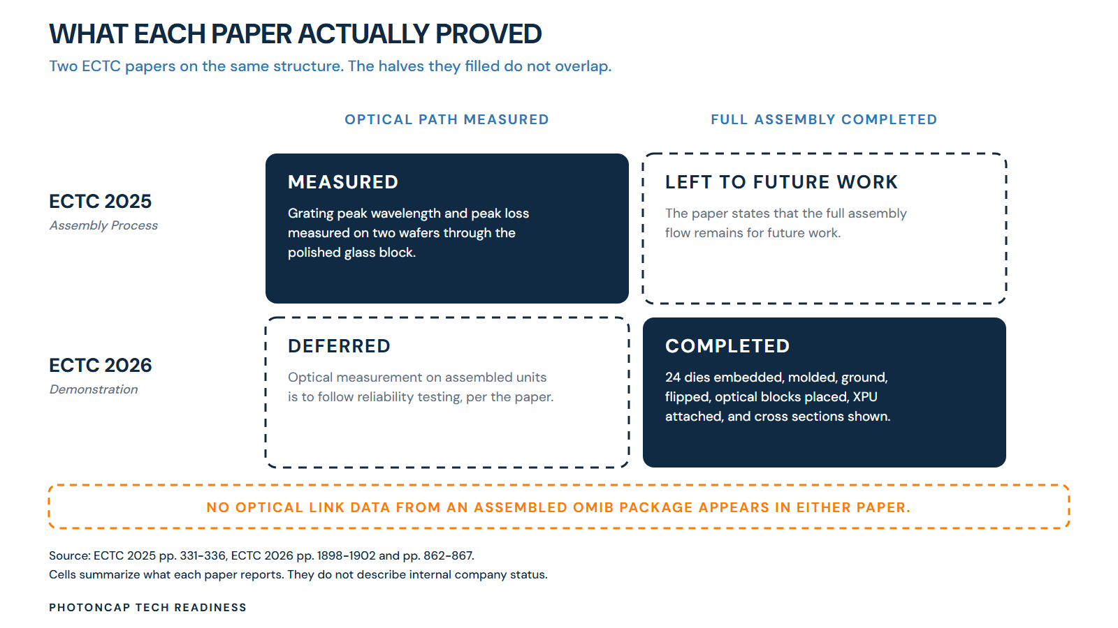
What each paper filled and what it left empty
8. Three Pieces, Three Stages
Calling Photonic Fabric one thing makes this distinction disappear. It is really three pieces, and each is at a different stage. This is a different split from the three product families the paper defines. I split it this way to organize the evidence.
Assembly. Proven end to end. There are cross section images, and the claim of compatibility with a standard back end flow is backed by the process sequence. But the subject was a passive test vehicle, and reliability results are not in the paper [3].
Link. Measured. Four TX and RX pairs on a 5 nm EIC, 56 Gb/s per channel, 2.8 pJ/bit energy efficiency on the electronic side, eye opening over 0.2 UI at the target error rate [4]. Good numbers. But these came off a different object. The paper says power was fed to the PIC by wire bond. This is a separate link demonstrator rather than the OMIB organic interposer structure.
System performance. All simulation. A 32 terabyte shared memory appliance cutting communication power by 60 to 90%, and throughput going up 5.6 times on a one trillion parameter model, belong here [4]. The simulator itself is reported as validated at about 8% mean error against real GPU hardware, but the appliance itself was not built and measured.
So the pieces each work, and they have not yet come together as one body. This is what it means for an option to have internal structure.
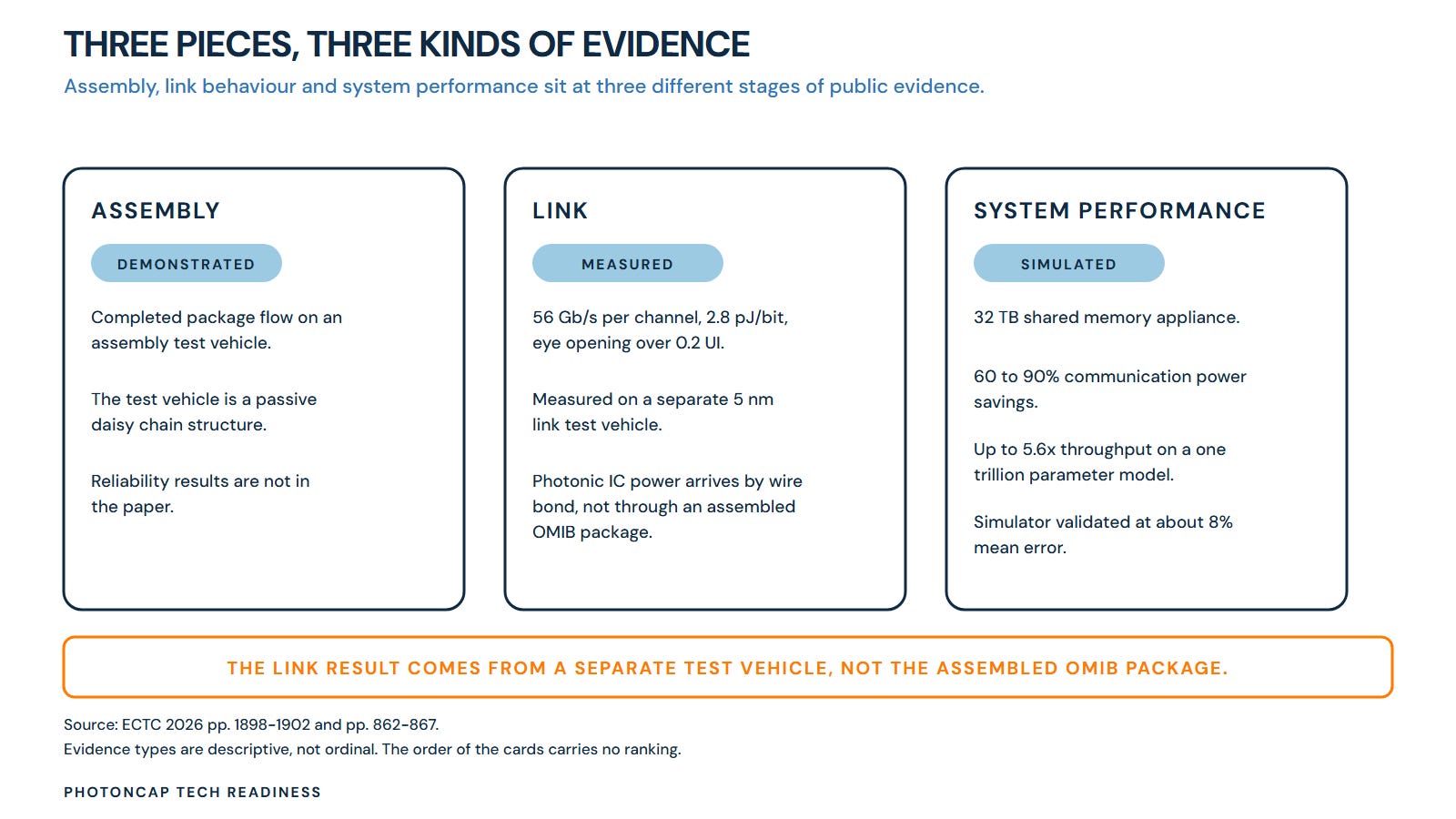
Assembly, link, and system performance, and the evidence grade of each
9. The Question With No Answer Yet
One of the things the paper does not cover keeps nagging at me.
The caption on the optical adhesive carries the word permanent. It means this is not a temporary protective material but a medium that stays in the final product for good, with the beam passing through it for its whole life. That makes yellowing, refractive index shift with temperature, moisture uptake, and delamination all lifetime items.
And EMC sits right next to that adhesive. The two materials have different coefficients of thermal expansion and shrink by different amounts as they cure. That boundary happens to be the edge of the optical aperture. When temperature cycles, stress concentrates exactly there.
The paper has no data on this item. Let me note that what follows is a failure hypothesis I constructed rather than something the paper proved. Even so, I think this is the real gate for this approach. Whether the assembly works has been answered, and the next question is how many years it holds.
10. Absence Is a Signal Too
An objection can be raised here. Not in the paper does not mean not at the company. That is fair. A paper is the floor of public evidence, not the ceiling of development progress.
But I read this case a little differently.
ECTC is the best conference in packaging. Marvell submitted papers there, and not one but several. So if there had been a result to show, they would have shown it there. Data showing an optical link running on an assembled package is a far stronger result than showing the assembly process works. From the position of choosing which papers to submit, there is no obvious reason to hold that result back and publish only the process story.
The timing has to be taken into account, of course. ECTC 2026 was held at the end of May, but paper submission comes several months before that. So what these papers reflect is the state as of early this year. Now, in August, they may have gone further.
But there is no public material telling us what moved how much in between. And what the paper wrote down is a sequence rather than a date. Reliability testing first, then measuring the assembled unit. Months can pass and that sequence still stands.
11. But the Product Lineup Is Already Out
Reading this far, something may feel off. The paper says the measurement has not happened, so what is the company doing?
On August 4 at FMS 2026, Marvell announced the Photonic Fabric product lineup [9]. Memory modules, a NIC, and a chiplet. The content is that it builds a shared memory tier across multiple racks, offloads up to 32 terabytes of warm KV cache, and raises token throughput by two to three times within existing data center footprint and power limits.
Two and a half months after the paper wrote “measurement after reliability testing.”
What is missing from the announcement matters too. There is no customer name. No sampling schedule and no production schedule either.
And how to read the number 32 terabytes is a question. The same number appears in the ECTC paper, where it is the capacity of the proposed appliance architecture and at the same time a configuration value fed into the system simulation. The table lists 32 terabytes of memory and 26.8 TB/s of network [4]. A result actually measured on 32 terabytes of hardware is not in the paper.
To be fair I should write one item the other way. The phrase two to three times on tokens is actually lower than the paper’s simulation. The paper put out up to 2.3 times at 405 billion parameters and up to 5.6 times at one trillion parameters. The same figure also carries 1.3 times and 1.4 times conditions. Marketing called it more conservatively than the paper did.
To put it together. The announcement and the paper move on different clocks. There is nothing strange about a company signaling its roadmap first, and papers are slow by nature. But you will get the timing wrong if you look at only one of them. The product announcement tells you where the company intends to go, and the paper tells you how far it has come.
12. What I Asked in April
In April of this year I wrote a piece called NVIDIA’s $2B Marvell Bet and Celestial AI’s “25x Bandwidth” Claim: What’s the Denominator?. I asked what the denominator was behind the 25x figure Celestial AI was putting forward, and at the time I could not find the answer.
The two OMIB papers carry that 25x and 10x wording in the introduction as is [3][5]. They still do not state the denominator.
What did arrive in the body are measured values. 56 Gb/s, 2.8 pJ/bit, 0.09 square millimeters of silicon per TX and RX pair. Converted to an HBM sized chiplet that comes to about 7.2 Tb/s, and the paper compares this against HBM3 at 6.5 Tb/s [4].
So April’s question got a partial answer. The denominator behind the marketing phrase is still unknown, but what the company has in mind as the comparison target came out in the papers. I think that was a reasonably well aimed question.
One more thing. The modulator choice I covered in the April piece and in The Truth Behind Marvell-Polariton: Is LWLG the First Candidate, or Just a Backup Bet? also got an answer this time. Photonic Fabric does not use micro rings. The paper even writes the reason, which is that their optical bandwidth is narrow and they are too temperature sensitive to sit next to a high power chip. It uses germanium silicon electro absorption modulators instead [4].
This is a choice that splits camps, so it is a subject that needs its own piece.
13. Closing
To compress the current state into one sentence, the pieces have each been proven and the data on the combined object has not come out yet. And the product has already been announced.
So I am holding my judgment. I lean positive, but the grounds to settle it have not been made public.
What is comfortable is that what to watch from here is clear. Two disclosures of different character are racing, and which one arrives first gives the answer.
One is on the paper side. The 2026 paper wrote the sequence down itself. Reliability testing first, then measuring the optics on assembled units. So the venues are set. OFC in the first half of 2027, and ECTC 2027 at the end of May or early June. Watch whether assembled unit optical data and reliability results show up there.
The other is on the business side. When the customer name and the sampling schedule that were missing from the August 4 announcement get filled in. The October 6 investor day is the nearest venue.
Before that there is the August 27 earnings release. What gets decided there is not the quarterly number but what comes up in the Q&A. Whether the customer name or the sampling schedule missing from the August 4 announcement gets mentioned, and whether the FY28 scale up optics outlook gets called up again. Calling it up would be a signal that the option value is being pulled forward, and leaving it alone means things are running in the sequence the papers drew. The revenue line itself will not decide it. Next to the $16.5B guide it is a rounding error [6].
The order of the two disclosures carries information. If reliability and optical data come first and customers attach after, it is rolling in the order I read. If instead customers and a production schedule are disclosed first, my understanding of the order is wrong, and it means the company is moving faster than what it publishes in papers. That is not bad news. It does mean the material I based this on is not keeping up with actual progress, and at that point I would have to move the basis of the judgment outside the papers.
And if next year’s conferences bring measurements on yet another test structure instead of assembled unit data, or if the reliability items start mentioning the adhesive and EMC boundary, the realization timing has to be pushed back. That stress concentrates at that boundary is my estimate rather than a value the paper measured, so until data comes out it is right to leave it as an open question.
To add one thing, what this piece covered is technical readiness, not this quarter’s numbers. However the earnings land a few days from now, the positions of the gates above do not change. Think of them as two clocks running on different layers.
Why buying and selling CPO at the ticker level does not work well is something I covered in an earlier piece, There Is No Such Thing as a ‘CPO Stock’: How the Market Misread SemiAnalysis, and this case is similar. It is closer to watching whether one gate opens than to buying one company.
Acknowledgment
One of the starting points for this piece is Damnang’s Marvell Part 3: What Has Been Proven, and What Is Still Open. That piece placed Photonic Fabric accurately at the earnings and valuation layer as “an option that is barely in the P&L yet,” and set the confirmation point at customer disclosure. This piece looks at the same question from the layer below, using different material. The two are not competing. They sit at different layers.
References
[1] Marvell Technology, “Marvell Completes Acquisition of Celestial AI,” 2026-02-02. https://www.marvell.com/company/newsroom/marvell-completes-acquisition-of-celestial-ai.html
[2] Marvell Technology, “Marvell to Acquire Celestial AI, Accelerating Scale-up Connectivity for Next-Generation Data Centers,” 2025-12-02. (Consideration structure as announced at the time of the deal) https://investor.marvell.com/news-events/press-releases/detail/1000/marvell-to-acquire-celestial-ai-accelerating-scale-up-connectivity-for-next-generation-data-centers
[3] D. Raorane, A. Aggarwal, S. Pothukuchi, S. Chadda, “Optical Multi-Chip Interconnect Bridge (OMIB) Interposer Demonstration to Enable High-density Photonic Interconnects for High-Performance Computing Applications,” 2026 IEEE 76th Electronic Components and Technology Conference (ECTC), pp. 1898-1902. DOI: 10.1109/ECTC51846.2026.00311
[4] D. Oh, A. Aggarwal, S. Pothukuchi, J. Pesic, S. Sahni, P. Mishra, G. Balamurugan, T. Diep, P. Winterbottom, D. Lazovsky, “Photonic Fabric Interconnect for a Scale-up Network Solution in Accelerated Computing,” 2026 IEEE 76th ECTC, pp. 862-867. DOI: 10.1109/ECTC51846.2026.00146
[5] A. Aggarwal, S. Pothukuchi, A. Rathi, S. Sahni, P. Winterbottom, D. Lazovsky, “Optical Multi-Chip Interconnect Bridge (OMIB) Interposer Assembly Process to Enable High-Density Photonic Interconnects for High-Performance Computing Applications,” 2025 IEEE 75th ECTC, pp. 331-336. DOI: 10.1109/ECTC51687.2025.00062
[6] Damnang, “Marvell Part 3: What Has Been Proven, and What Is Still Open,” 2026-08-21. (Secondary source. Company guidance figures are cited as compiled in that piece)

[7] J. F. Dillon, T. Zheng, A. Vohra, K. Blacklow, E. Tremble, W. Sauter, S. Allman, “Marvell custom HBM routing and signal integrity analysis,” 2026 IEEE 76th ECTC, pp. 298-303. DOI: 10.1109/ECTC51846.2026.00055
[8] Y. Mekonnen, J. Xie, Z. Qian, X. Konstantinou, Y. Si, Y. Cui, K. Aygün, K. Radhakrishnan, “Enabling 12+Gb/s HBM4E with EMIB-T Advanced Packaging Technology,” 2026 IEEE 76th ECTC, pp. 455-460. DOI: 10.1109/ECTC51846.2026.00078
[9] Marvell Technology, “Marvell Advances AI Memory Infrastructure Portfolio to Accelerate Agentic AI Inference,” 2026-08-04. https://investor.marvell.com/news-events/press-releases/detail/1030/marvell-advances-ai-memory-infrastructure-portfolio-to-accelerate-agentic-ai-inference
This article is an independent technical analysis published by PhotonCap, based on an engineering perspective. All content is derived from publicly available information and is intended solely for educational and informational purposes. In other words, nothing in this material should be construed as a recommendation to buy, sell, or hold any specific securities. Please note this carefully.
The author may hold positions in the securities mentioned herein and reserves the right to trade such securities at any time without prior notice. Readers should conduct their own thorough review and research before making any investment decisions.
Excellent piece, PhotonCap. I really appreciate the way you separate the architecture into the parts that have actually been demonstrated from the parts that still need to be proven.
The top-entry approach is fascinating, but your analysis makes the timing question much clearer: meaningful engineering progress has been made, while the decisive assembled-system evidence is still ahead. That distinction is especially useful for anyone trying to understand where photonic fabric actually sits on the road from promising architecture to investable commercial reality.