
NVIDIA's $2B Marvell Bet and Celestial AI's "25x Bandwidth" Claim: What's the Denominator?

Abstract
In March 2026, NVIDIA invested a total of $6B across Lumentum (LITE), Coherent (COHR), and Marvell (MRVL). This article decomposes the three investments by Scale-Up / Scale-Out / Scale-Across layer and analyzes the structural purpose of each deal. The focus is Celestial AI’s Photonic Fabric technology, acquired by Marvell for $3.25B. We examine the measurement basis behind the “25x bandwidth vs. CPO” claim and analyze three engineering resistance points on the path to volume production: yield, light source integration, and thermal management. A scenario-based value chain beneficiary/risk positioning map shows the asymmetric upside structure of LITE/COHR and the high-variance position of MRVL.
Contents
Intro
Background: Three Stages of AI Infrastructure Scaling
Section 1: NVLink Fusion, Why NVIDIA Opened Its Proprietary Interconnect
Section 2: Why Marvell Became the First NVLink Fusion Partner
Section 3: Celestial AI Photonic Fabric, the Technology and the Distance to Volume Production
Section 4: LITE + COHR, Why NVIDIA Locked Down the Laser Supply Chain
Section 5: Strategic Structure Analysis, the $6B Blueprint
Insights / Investment Implications
Closing
References & Sources
Intro
Three pieces of news dropped before March was even over.
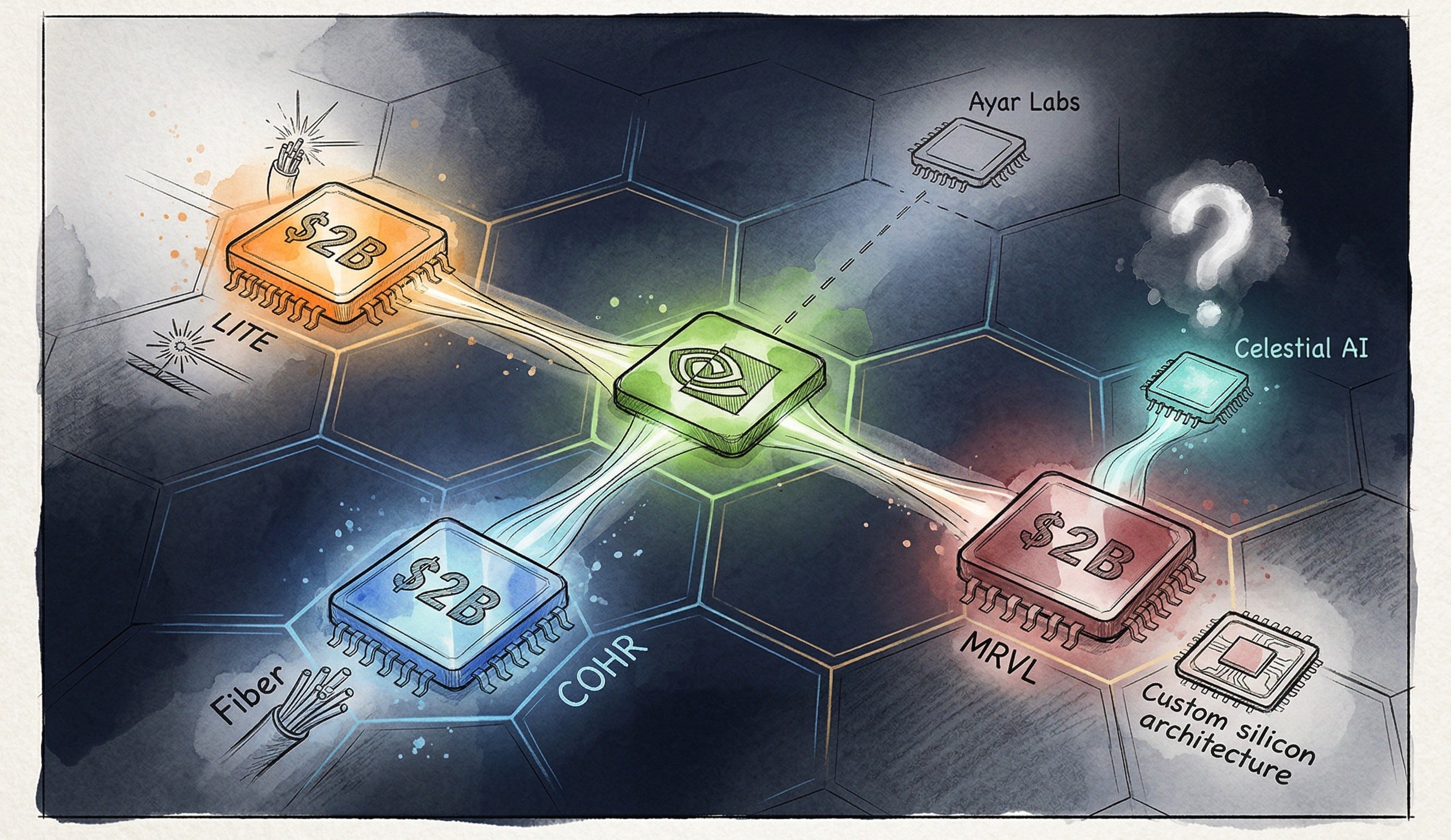
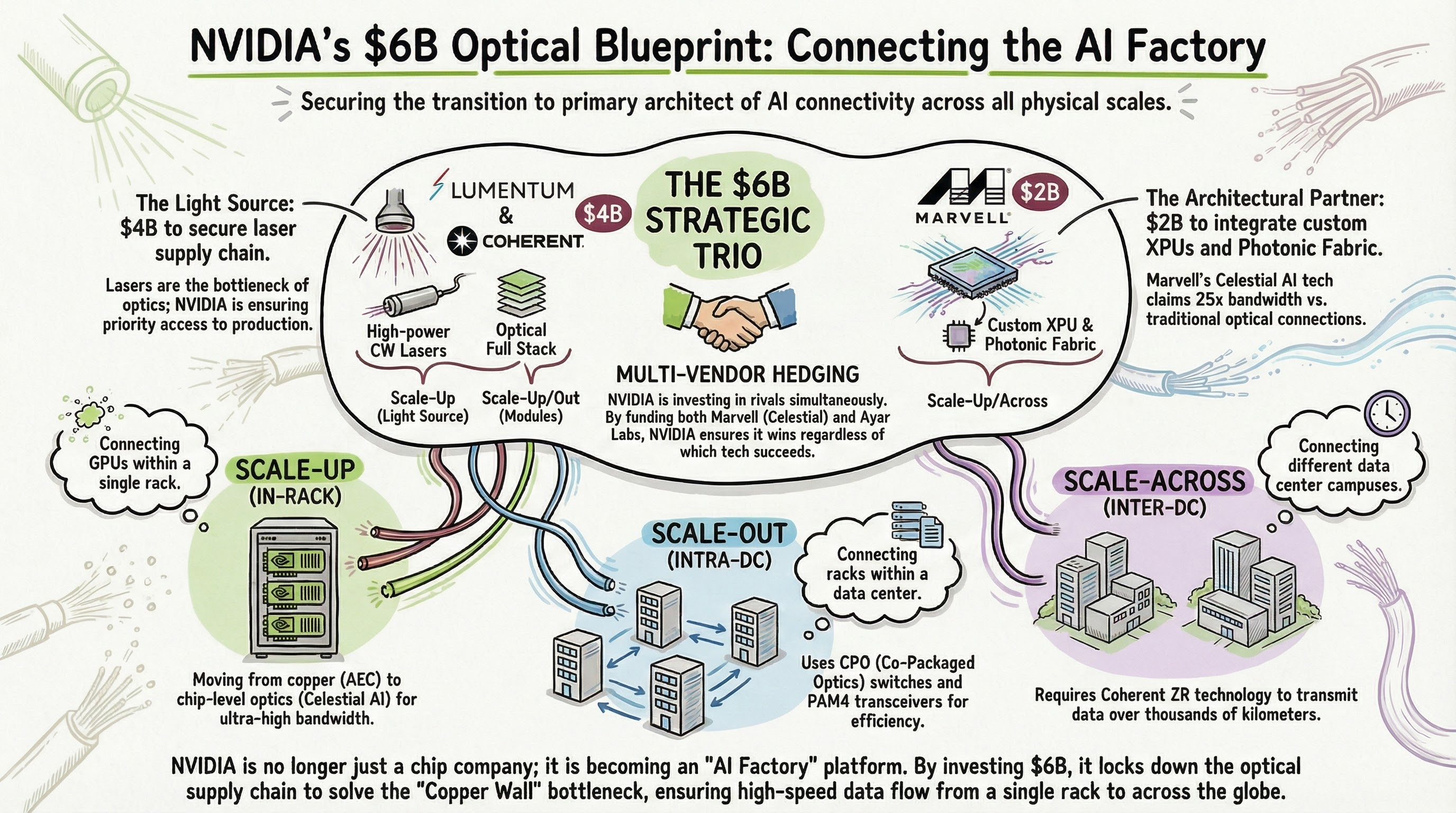
On March 2, NVIDIA announced a $2B investment in Lumentum Holdings (NASDAQ: LITE). The same day, another $2B into Coherent Corp (NYSE: COHR).[1][2] On March 31, an additional $2B into Marvell Technology (NASDAQ: MRVL).[3]
$6B in a single month. All directed at photonics and optical interconnect infrastructure.
If you read these numbers as simply “NVIDIA locking down the optical supply chain,” you’re only seeing half the picture. Here’s the thesis of this article.
NVIDIA is transitioning from a company that sells GPUs to a platform company that designs the entire connectivity architecture of the AI factory. And photonics is going into every layer of that architecture.
To see this structure clearly, you first need to understand three scaling concepts, and then take a separate look at the Celestial AI technology bet tied to Marvell. In particular, Celestial’s claim of “25x bandwidth and 10x lower latency versus CPO” needs to be examined with proper context.
Today we map the full $6B investment structure layer by layer, and analyze the Celestial AI technology at the core of the Marvell deal from an engineering perspective.
Background: Three Stages of AI Infrastructure Scaling
Scale-Up, Scale-Out, Scale-Across: They Sound Similar but They’re Completely Different Problems
There are three directions for scaling AI infrastructure. This distinction forms the backbone of the entire article, so let’s get it right up front.
Scale-Up is the approach of connecting accelerators more tightly within a single compute domain. Inside a single rack, GPUs or XPUs are bound together through a unified memory-semantic fabric so they operate as one massive compute engine. NVIDIA’s NVLink is the canonical example. Connection distances range from meters to tens of meters, and copper (AEC, Active Electrical Cable) can physically handle these distances.[5]
Scale-Out is the stage of connecting rack to rack within a data center. InfiniBand and Ethernet are the primary protocols, and distances extend from tens to hundreds of meters. Copper can’t keep up, and PAM4-based optical transceivers (400G, 800G, 1.6T) become essential. This is precisely why CPO (Co-Packaged Optics) switches are gaining traction.[5]
Scale-Across is data center to data center, campus to campus, region to region connectivity. Distances stretch from 2 km to thousands of kilometers. Without coherent ZR/ZR+ technology, this is simply not possible. As AI models begin exceeding the power limits and physical space of a single data center, demand at this layer is growing rapidly.[6]
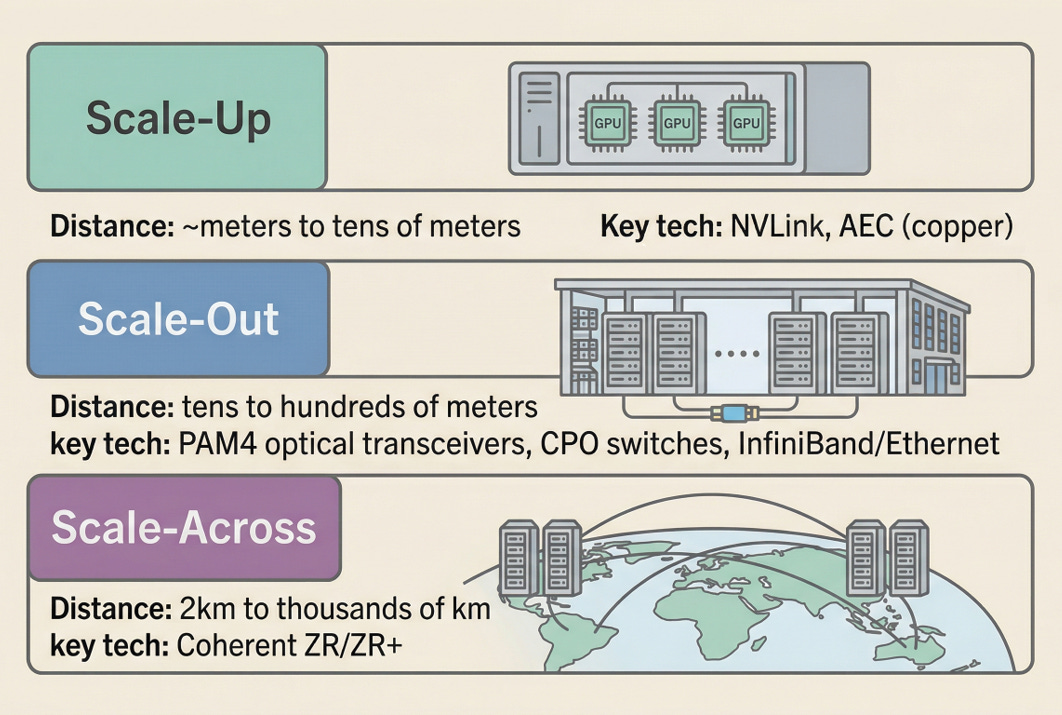
Each layer demands completely different specifications for bandwidth, latency, and power efficiency. Scale-up requires multi-TB/s ultra-low-latency fabrics. Scale-out prioritizes switching capacity and energy efficiency. Scale-across depends on coherent modulation capable of surviving hundreds to thousands of kilometers.
Map NVIDIA’s $6B worth of partners onto these three layers, and the investment structure becomes much clearer.
NVIDIA’s $6B optical investment is not simply supply chain insurance. It is a structural design to bind optical architecture to its own ecosystem across every layer, from scale-up to scale-across.
Section 1: NVLink Fusion, Why NVIDIA Opened Its Proprietary Interconnect
NVLink’s Role: Making the Entire Rack Act as One GPU
NVLink is the high-speed direct-connect fabric between NVIDIA GPUs. If PCIe is a peripheral bus connecting GPUs to the CPU, NVLink is a memory-semantic interconnect that lets GPUs communicate directly as if sharing memory.
The Blackwell generation’s NVLink 5 supported 1.8 TB/s bidirectional bandwidth per GPU. In the GB200 NVL72 rack, connecting 72 GPUs in an all-to-all topology yields 130 TB/s of aggregate bandwidth.[7] That’s one NVLink domain, and NVIDIA describes GPUs within this domain as operating like a single massive accelerator.
The Rubin generation steps up to NVLink 6. Bandwidth doubles to 3.6 TB/s bidirectional per GPU, and the Vera Rubin NVL72 rack supports a total of 260 TB/s of scale-up bandwidth.[8] For model architectures like MoE (Mixture-of-Experts) where all-to-all communication is frequent, this bandwidth difference directly translates to processing speed.
NVLink Fusion: Open the Ecosystem, but I Write the Rules
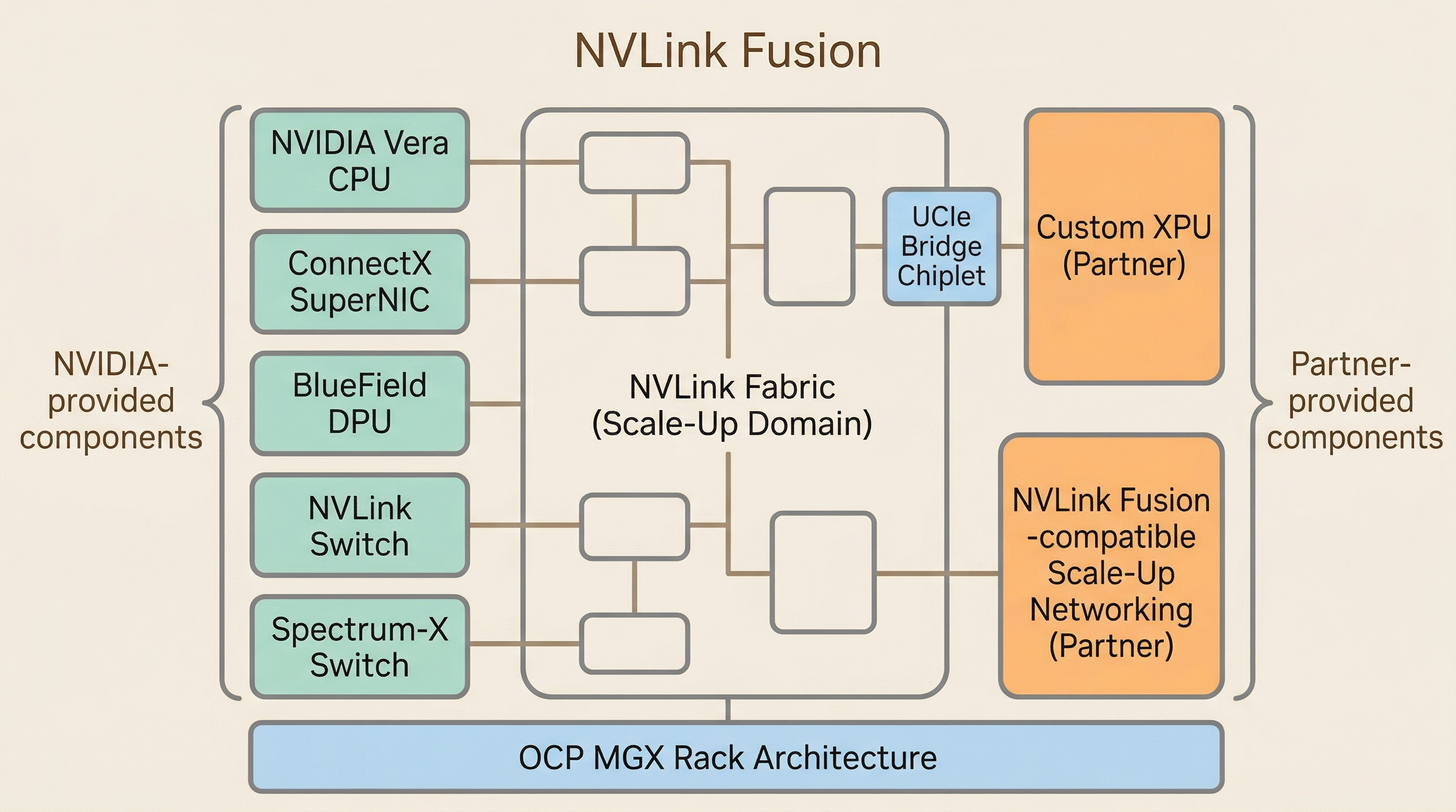
NVLink used to be a proprietary interconnect exclusive to NVIDIA GPUs. Starting in 2025, NVIDIA began opening this fabric to third-party silicon under the name NVLink Fusion.[4][9]
Here’s how it works. External XPUs connect to the NVLink fabric through a UCIe (Universal Chiplet Interconnect Express) bridge. NVIDIA provides the UCIe-to-NVLink bridge chiplet, and XPU designers can operate within the same scale-up fabric alongside NVIDIA GPUs.[9] In the NVLink Fusion ecosystem, NVIDIA provides the Vera CPU, ConnectX SuperNIC, BlueField DPU, NVLink interconnect and switches, Spectrum-X switches, and OCP MGX-based rack architecture. Partners layer custom XPUs and NVLink Fusion-compatible scale-up networking on top.[3]
Why open a proprietary fabric? Hyperscalers (Amazon, Google, Microsoft, etc.) are already deploying their own custom AI accelerators. Trainium, TPU, Maia. They have the motivation to route around NVIDIA’s expensive GPUs. At the same time, the UALink consortium, led by AMD, Intel, Google, Microsoft, AWS and others, is pushing an open interconnect standard.[26]
Copper Wall, Age of Light — Dissecting Marvell's FY2026 & the 1.6T Optics Chain

Every time AI semiconductors come up, it’s always the same three names: Nvidia, AMD, Broadcom. Important companies, sure. But I think the real money is increasingly moving elsewhere.
NVIDIA’s response: “Don’t use my GPU if you don’t want to. But play inside my NVLink fabric.” Hyperscalers get to use custom silicon optimized for their workloads while keeping NVIDIA’s software stack and proven rack architecture. NVIDIA, in turn, holds the interconnect standard and maintains attach rate (the ratio of ancillary product and service revenue per GPU sale) on NICs, DPUs, switches, and software.
NVLink Fusion is not about maximizing GPU sales. It’s a structure for NVIDIA to keep defining the AI factory architecture standard. It looks open, but NVIDIA writes the rules of that openness.
Section 2: Why Marvell Became the First NVLink Fusion Partner
The Position Fits Perfectly
In this deal, Marvell provides two things: NVLink Fusion-compatible custom XPUs and NVLink Fusion-compatible scale-up networking. The partnership also includes AI-RAN collaboration for 5G/6G telecom infrastructure, but this article focuses on optical interconnects.[3]
To understand “why Marvell,” you need to look at what portfolio they’ve built over the past 3 to 4 years. Marvell started as a communications semiconductor company and has transformed into one covering the full scope of data center AI infrastructure. In FY2026, data center revenue accounted for 74% of total revenue ($6.1B), and total revenue grew 42% year-over-year to $8.2B.[10] In custom XPU programs (contract design of hyperscaler custom silicon, such as Google TPU), they’ve built a substantial track record. As of the FY2026 earnings, over 18 XPU and XPU-attached sockets are in volume production, and a pipeline of over 50 new design opportunities is in progress with more than 10 customers.[10]
Their optical DSP portfolio fills all three scale layers:
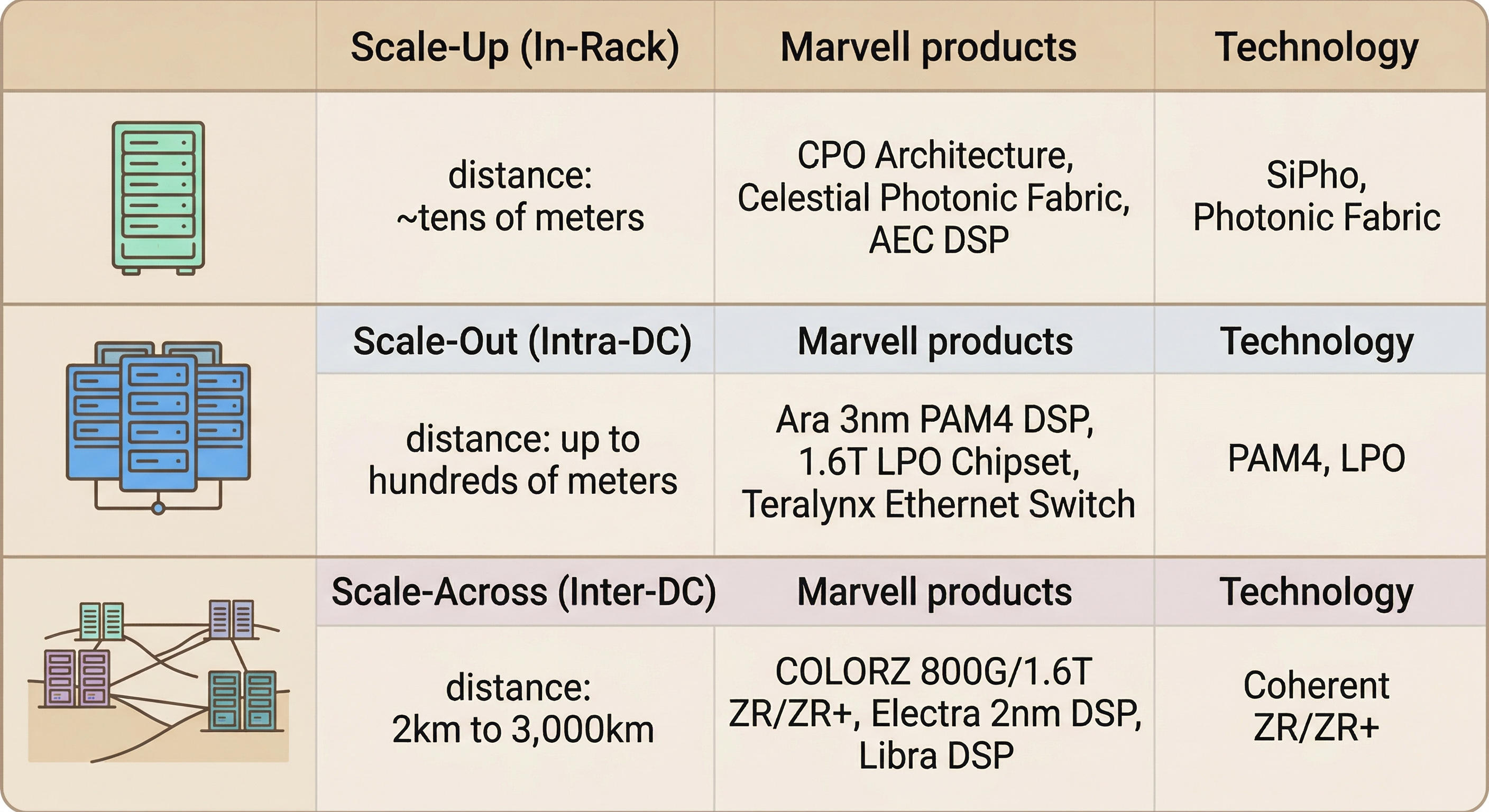
A semiconductor company that covers all three scale layers with an optical portfolio is rare in the industry.
Celestial AI Acquisition: A Major Bet on Scale-Up Optics
In December 2025, Marvell announced the acquisition of Celestial AI for $3.25B ($1B cash + $2.25B stock), and the deal closed in February 2026.[11]
The technology Celestial AI developed is a platform called Photonic Fabric. At its core is OMIB (Optical Multi-Chip Interconnect Bridge), an optical die-to-die interconnect technology that handles package-level, system-level, and rack-level connections entirely through optics.[11] Marvell’s thesis is that this technology can break through the physical limits of copper in the scale-up domain.
For context, the 9-meter 800G AEC that Marvell and Infraeo demonstrated at the OCP Global Summit is symbolic.[12] Pushing copper to 9 meters is an impressive achievement. Previous 800G AEC products topped out at 3 to 5 meters, and nearly doubling that distance to the maximum demonstrated at a conference means we’re looking at the ceiling of current technology. At the same time, it signals that copper can’t go much further. PAM4 signals suffer sharply increasing attenuation in copper as frequency rises, and extending distance requires additional power and retimers to compensate. 9 meters is effectively the upper bound of what copper can sustain at 800G with current technology. As XPUs scale from tens to hundreds within a scale-up domain, the transition from copper to optics is a physical inevitability.[5]
Celestial’s Photonic Fabric targets exactly that inflection point. Marvell plans to integrate it into their custom XPU architecture, designing scale-up domains that connect hundreds of XPUs across racks using optics.[13]
Marvell being chosen as the first NVLink Fusion partner is not a coincidence. Custom XPU design capability, an optical DSP portfolio covering all three layers, and the next-generation scale-up optical technology secured through the Celestial AI acquisition all lined up at once.
