
I Read 24 Papers. The Press Releases Were Lying. Why Samsung, NVIDIA, Broadcom, and Meta Were All at the Same Conference: A Non-Specialist’s Interpretation
$NVDA $AVGO $GFS $COHR $LITE $MRVL $GLW $META $MSFT $CIEN $CSCO $NOK | Samsung, Lightmatter, Furukawa, Sumitomo

Press Releases Are Marketing. Papers Are Physics.
Companies can say whatever they want in a PR. “Industry first.” “Breakthrough performance.” “Next-generation platform.” But in a conference paper, the physics has to hold up. Or you get corrected.
That’s why I read the papers, not the press releases.
OFC (Optical Fiber Communication Conference) is the photonics equivalent of ISSCC, IEDM, and VLSI in semiconductors. Together with ECOC and CLEO, it forms the top three photonics conferences in the world. These aren’t venues where companies publish to hide. These are venues where companies publish to show off their best work.
Look at the graphs. Check the physics. Find the gap between the marketing and the math. That’s what I do.
It’s been over a month since OFC 2026 wrapped, but I’ve finally completed my analysis of all 24 papers across a 5-part series. SiPh foundries, CPO and AI interconnects, glass substrates and advanced packaging, coherent and pluggables, and hollow-core fiber. This is the first time I’ve studied this many papers from a single conference. It took longer than expected. The telecom systems papers in particular were tough since that’s not my specialization. Unfamiliar terminology, unfamiliar conventions. Even with AI tools, there were plenty of gaps I had to fill on my own. Realistically, reviewing 3 papers a night after work was a productive day.
If you don’t have the time or the background to read the papers yourself, that’s what PhotonCap is for.
So What Did I Find?
In March 2026, NVIDIA invested $2B in Lumentum, $2B in Coherent, and $2B in Marvell. $6B total poured into the optical value chain in a single month. Why?
NVIDIA's $4 Billion Photonics Bet: Broadcom Wasn't Wrong — But the Market Completely Misread the Signal

1. Introduction: The Announcement and the Market’s Reaction

Because no matter how fast GPUs get, if the speed at which GPUs talk to each other can’t keep up, the entire system stalls.
The next bottleneck after GPUs is optics. And whoever controls that optical layer, and how, will determine the next chapter of AI infrastructure.
The 24 papers from OFC 2026 map the current coordinates of this war. Samsung, NVIDIA, Broadcom, Meta, Cisco, Nokia, Corning, and Microsoft were all talking about the same problem. Except the papers contained things the press releases didn’t show.
This article interprets the five technology fronts revealed by those 24 papers, at a level accessible to investors and non-specialists.
OFC 2026 at a Glance: Five Fronts
The optical infrastructure of AI data centers splits into five technology layers. OFC 2026 was a rare year where significant papers appeared across all five.
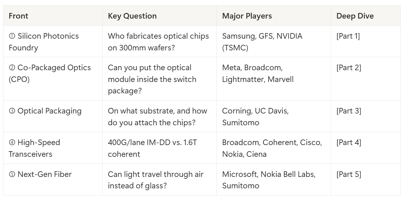
These five fronts are not independent. Optical chips from the foundry (①) get assembled via packaging (③) into CPO engines (②), pass through transceivers (④), and send data over fiber (⑤). If one link breaks, the whole chain breaks.
Front ①: Silicon Photonics Foundry: “Who Makes the Optical Chips?”
[OFC 2026] Part 1 of 5: 300mm SiPh Foundry: Who Is Actually Ready?
![[OFC 2026] Part 1 of 5: 300mm SiPh Foundry: Who Is Actually Ready?](https://substackcdn.com/image/fetch/$s_!zc4V!,w_1300,h_650,c_fill,f_webp,q_auto:good,fl_progressive:steep,g_auto/https%3A%2F%2Fsubstack-post-media.s3.amazonaws.com%2Fpublic%2Fimages%2F22cba2f2-fc29-43bd-b592-166665f23944_2949x1557.png)
Two Ways to Read a Conference Paper
When you think semiconductor foundry, TSMC comes to mind. But the “optical semiconductor” foundry is a different game.
Regular semiconductors move electrons. Optical semiconductors move light. Instead of transistors, you have modulators, photodetectors, and waveguides. Different manufacturing processes, different design ecosystems.
At OFC 2026, Samsung, GlobalFoundries (GFS), and NVIDIA each unveiled their 300mm silicon photonics (SiPh) platforms. Seven papers total. But between the numbers in the papers and reality, there were gaps.
Samsung publicly disclosed its full 300mm SiPh platform for the first time. Modulators, photodetectors, a PDK (process design kit) with 40+ components. Impressive. But the key photodetector (APD) requires -6.1V to operate. The electronic IC (EIC) it pairs with runs at 1.8V max. There’s a disconnect between the “low-voltage” marketing and actual system requirements.
NVIDIA presented MRM (micro-ring modulator) design theory based on TSMC’s photonics-dedicated process (COUPE). This came right after the world’s first 1.6Tbps CPO switch demo at GTC 2025. But dig into the paper, and the coefficient of determination (r²) for MRM manufacturing variability is 0.49. More than half the variation is unexplained.
GFS showed 200Gbps PAM4 operation. The most substantive data of the three. Though the noise floor of the test infrastructure itself was masking the device performance.
The numbers are right. The interpretation is different. Deep dive: [Part 1: 300mm SiPh Foundry: Who Is Actually Ready?]
Front ②: CPO: “Putting the Optics Inside the Chip Package”
[OFC 2026] Part 2 of 5: CPO and the AI Interconnect Challenge
![[OFC 2026] Part 2 of 5: CPO and the AI Interconnect Challenge](https://substackcdn.com/image/fetch/$s_!AyZ0!,w_1300,h_650,c_fill,f_webp,q_auto:good,fl_progressive:steep,g_auto/https%3A%2F%2Fsubstack-post-media.s3.amazonaws.com%2Fpublic%2Fimages%2Fe8cfa0e1-324d-4732-840c-816b5743b108_2949x1557.png)
AI clusters are doubling in scale every year. Meta’s current ORv3 rack connects 72 GPU nodes over a copper backplane. The ORW rack, soon to be deployed, scales to 144 nodes. The next generation exceeds 256 nodes, pushing single-rack power past 1 MW [1]. At this scale, copper-based electrical interconnects hit walls simultaneously across power, bandwidth density, and routing complexity.
Today, optical modules in data centers are “pluggable”: you insert them into the front panel of a switch. Electrical signals travel from the switch chip across the board to the front panel, where they’re converted to light. The problem: the longer that electrical path, the more power is wasted and the harder it is to maintain speed.
CPO (Co-Packaged Optics) puts the optical module right next to the switch chip. The idea is to radically shorten the electrical path to capture both power and bandwidth gains simultaneously.
Meta released long-term reliability data for a CPO switch at OFC 2026. They ran 15 units of Broadcom’s Bailly 51.2Tbps CPO switch for nine months, accumulating 36 million device-hours. They reported 65% optical power savings.
But here’s the catch. What Meta tested was a “scale-out” switch for data center interconnect. Not the “scale-up” GPU-to-GPU ultra-short-reach connections that AI training demands. And that scale-up domain is where the real CPO battle will be fought.
Lightmatter demonstrated 800Gbps/fiber at 3.8 pJ/bit on a GFS-foundry MRM CPO. Furukawa presented an external laser source. Marvell showed a next-generation photodetector. The pieces of the CPO value chain are coming together, but the full picture isn’t complete yet.
CPO has entered the stage where it must prove operational viability, not just performance. And there are still significant gaps. Deep dive: [Part 2: CPO and the AI Interconnect Challenge]
Front ③: Optical Packaging: “Light on Glass”
![[OFC 2026] Part 3 of 5: Packaging: Glass Substrates to 3D Hybrid Bonding](https://substackcdn.com/image/fetch/$s_!tElU!,w_1300,h_650,c_fill,f_webp,q_auto:good,fl_progressive:steep,g_auto/https%3A%2F%2Fsubstack-post-media.s3.amazonaws.com%2Fpublic%2Fimages%2Ff9a73981-8047-4f7a-9f68-d64d56d2d650_2949x1557.png)
No matter how good the chip is, if you can’t mount it on a substrate and connect it to fiber: the “packaging”: it’s useless. And conventional organic substrates (PCBs) aren’t suited for optical chips. The coefficient of thermal expansion doesn’t match, and the optical alignment precision isn’t there.
Corning brought glass substrates to the table. Build optical waveguides on glass, then mount optical chips on top. You might wonder why Corning: famous for Gorilla Glass: is suddenly entering semiconductor packaging. The answer is simple. Glass has a lower CTE than silicon, is optically transparent, and can be manufactured at large scale. It could become the “next substrate” for semiconductor packaging.
UC Davis presented hybrid bonding (directly bonding copper pads without solder) to stack optical and electronic chips in 3D. This is exactly the technology TSMC’s COUPE process uses.
Sumitomo demonstrated heterogeneous integration of InP optical chips directly on silicon. 80% footprint reduction, 800G performance achieved.
All three approaches point the right direction. Production evidence is still missing. Deep dive: [Part 3: Packaging: Glass Substrates to 3D Hybrid Bonding]
Front ④: High-Speed Transceivers: “The 400G/Lane Wall and the 1.6T Power Envelope”
![[OFC 2026] Part 4 of 5: 400G/Lane and 1.6T Coherent: Two Fronts, One Power Wall](https://substackcdn.com/image/fetch/$s_!XldD!,w_1300,h_650,c_fill,f_webp,q_auto:good,fl_progressive:steep,g_auto/https%3A%2F%2Fsubstack-post-media.s3.amazonaws.com%2Fpublic%2Fimages%2Fee56b9ef-b096-4e42-a303-7bfc3075ac15_2949x1557.png)
Transceivers convert electrical signals to light (transmit) and light back to electrical signals (receive). They’re the critical components connecting within and between data centers.
Two fronts are racing simultaneously.
First: the 400G/lane competition inside data centers. Broadcom achieved 99GHz bandwidth on an InP-based EML (electro-absorption modulated laser). Coherent Corp analyzed the 400G/lane link budget and showed that receiver sensitivity degrades by about 5dB going from 200G to 400G. 5dB is a 3x difference in power. Not an easy gap to close.
Second: the 1.6T coherent competition between data centers. Nokia, Cisco, and Ciena each presented 1.6T pluggable roadmaps from different angles. The interesting part: Cisco, the #1 player in 800G coherent, did not announce a single 1.6T product at OFC 2026. Look at the MDL (Modulation-Dependent Loss) and driver power tradeoff data Cisco published in their paper, and you can see why they need more time.
Ciena proposed a new category called FST (Full-Spectrum Transponder). The concept: fill the entire C/L-band from Day 1 with a single transponder. When CPO eats the short-reach optics inside routers, line-side coherent optics will move back outside the router. FST targets exactly this structural shift.
400G/lane IM-DD and 1.6T coherent are different fronts, but they’re hitting the same wall. Power. Deep dive: [Part 4: 400G/Lane and 1.6T Coherent: Two Fronts, One Power Wall]
Front ⑤: Next-Gen Fiber: “Light Through Air”
[OFC 2026] Part 5 of 5: Hollow-Core Fiber and Next-Gen Transmission: Beyond the Loss Record
![[OFC 2026] Part 5 of 5: Hollow-Core Fiber and Next-Gen Transmission: Beyond the Loss Record](https://substackcdn.com/image/fetch/$s_!1GzS!,w_1300,h_650,c_fill,f_webp,q_auto:good,fl_progressive:steep,g_auto/https%3A%2F%2Fsubstack-post-media.s3.amazonaws.com%2Fpublic%2Fimages%2F88d3b6d6-2bdd-4ca2-9142-caebbf7490e9_2949x1557.png)
Hollow-Core Fiber (HCF) has carried the label “someday technology” for years. Loss records were broken annually, and lab demonstrations piled up. But the mood at OFC 2026’s Th1J and W1F sessions is different. Microsoft, Nokia Bell Labs, and Sumitomo Electric are each answering the same question from different angles.
The world’s communication networks run on optical fiber made of silica glass (SMF). A technology used for nearly 50 years, and it works well. But there are physical limits. Light interacting with the glass medium creates nonlinear distortion, and that becomes the ceiling for long-haul, high-capacity transmission.
HCF (Hollow-Core Fiber) is optical fiber where light travels through air, not glass. Nonlinearity drops to 1/2,600th of conventional fiber. In theory, you can go much farther at the same power.
Microsoft’s Azure Fiber team demonstrated 442km HCF transmission: the world’s first using real-time commercial transceivers. Nokia Bell Labs analyzed the optimal ratio for hybrid configurations mixing HCF with conventional SMF. Sumitomo estimated 1 Pb/s (petabit) capacity from a 2-core fiber for submarine cables.
The practical challenges for HCF are cost and manufacturing. Current HCF pricing is tens of times higher than SMF, and splicing technology isn’t mature yet. But the fact that Microsoft is running large-scale transmission experiments itself signals that this technology is moving from “someday” to “within a few years.”
HCF has moved past the loss-number competition and entered the operational viability proof stage. Deep dive: [Part 5: Hollow-Core Fiber: Light Through Air]
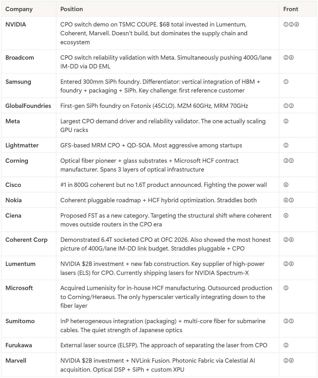
Who’s Fighting Where: Company Positioning Map
Why This Matters Right Now
Three trends are happening simultaneously.
First, AI clusters are getting bigger. According to Meta, GPU racks are expanding from 72 nodes (ORv3) to 144 nodes (ORW) to 256+ nodes. As nodes increase, GPU-to-GPU communication bandwidth grows exponentially, and existing copper wiring hits its limits in both power and bandwidth.
Second, optics is shifting from “optional” to “essential.” Until now, optics was used for data center interconnect (kilometers to thousands of kilometers). Now optics is moving inside the data center, inside the rack, and even between chips. CPO is the vanguard of this transition.
Third, the value chain is being reshuffled. NVIDIA doesn’t make optical chips itself, but invested $6B in Lumentum, Coherent, and Marvell in a single month, effectively pre-empting the optical supply chain. Broadcom straddles both CPO and IM-DD. Corning: the original optical fiber company: is positioning across glass substrates and HCF contract manufacturing, covering the full optical infrastructure stack. Microsoft is vertically integrating down to self-manufactured fiber. The existing optical value chain, the semiconductor value chain, and the hyperscalers are colliding in a three-way contest.
This is as far as the map goes with publicly available information.
But maps alone don’t win wars. The actual numbers each company showed in their papers, how those numbers differ from PR, and the structural patterns that only emerge from cross-analyzing all 24 papers: you only get that by reading the papers directly.
From here:
Why Samsung’s vertical integration is a different game from GFS/TSMC (Insight 1)
How Coherent and Lumentum survive in the CPO era (Insight 2)
The real meaning of NVIDIA’s $6B investment: “Optical CUDA” (Insight 3)
Why Corning spans optical fiber, glass substrates, and HCF contract manufacturing simultaneously (Insight 4)
The market that paradoxically grows when CPO succeeds (Insight 5)
Microsoft’s unprecedented vertical integration down to the fiber layer (Insight 6)
Three inflection points to watch
24 papers. One month of analysis. The free section showed you “what’s there.” The paid section is “how to interpret it.”
Insight 1: The SiPh Foundry Race Splits Along Two Axes: “Device Performance” and “Vertical Integration”
Samsung, GFS, and NVIDIA (TSMC) all published impressive device performance numbers at OFC 2026. But line them up side by side, and it’s not a simple spec race. Each player has fundamentally different strengths.
GFS published performance data alongside a simulation platform (Photonic-Native Compact Modeling) co-developed with Cadence. An environment where IC designers can run electro-optical co-simulation without learning a separate photonic simulator. GFS already has real customers (Lightmatter, Marvell estimated) on its Fotonix platform. It has a design ecosystem lead from its head start. But GFS doesn’t make memory, and its advanced packaging capabilities are limited.
TSMC has the most aggressive roadmap in optical foundry with COUPE, and has secured NVIDIA as a powerful first customer. It also has best-in-class packaging with CoWoS/SoIC. But TSMC doesn’t make memory. If you need HBM, you source it separately from SK hynix or Samsung.
What’s interesting about Samsung is that it entered the SiPh foundry business relatively recently, yet unveiled a full platform with 40+ PDK components at OFC 2026. Fast execution. But Samsung’s real differentiator isn’t device specs. It’s the vertical integration: HBM memory, logic foundry, advanced packaging, and now silicon photonics, all from a single company. In the CPO era, GPU + HBM + optical engine will sit inside a single package. The only foundry that can provide all three under one roof, as a turnkey solution, is Samsung.
Tower Semiconductor (TSEM) is an Israel-based specialty foundry with long SiPh experience, but lacks its own advanced packaging capabilities. No memory either.
Takeaway: The SiPh foundry race isn’t a simple spec battle. Three strategies are colliding: “design ecosystem first” (GFS), “anchor customer + packaging lead” (TSMC), and “vertical integration turnkey” (Samsung). Samsung’s challenge is landing its first reference customer. If it does, the HBM + SiPh + packaging bundle becomes a formidable weapon.
Insight 2: CPO’s Real Competitor Is “Improved Pluggables”
Market expectations for CPO are high. But cross-analyzing OFC 2026 papers reveals that CPO’s real hurdle isn’t technology: it’s economics.
Meta repeated three conditions in their paper. For optics to replace copper, it must be (1) as cheap as copper, (2) as power-efficient as copper, and (3) as reliable as copper. Accumulating 36 million device-hours of reliability data is progress toward (3). But (1) and (2) remain unproven.
Meanwhile, Ciena’s paper showed through simulation that intermediate stages like LPO (Linear-drive Pluggable Optics) and NPO (Near-Packaged Optics) can work adequately even at 200G/lane. Before CPO becomes the “final answer,” improved pluggables can buy time.
But here’s an important nuance. Classifying companies like Coherent and Lumentum as “pluggable value chain only” would be wrong. Coherent demonstrated a 6.4T (32×200G) socketed CPO on SiPh at OFC 2026, and Lumentum supplies CPO lasers alongside NVIDIA. These companies straddle both pluggable and CPO. They generate current revenue from pluggables while simultaneously preparing for the CPO era: a “both legs” strategy.
Takeaway: If CPO adoption is slow, pluggable revenue extends. If fast, CPO revenue ramps sooner. For Coherent and Lumentum, there’s business either way. The real risk isn’t transition speed: it’s losing the battle over “whose optical engine becomes the standard” in the CPO era.
Insight 3: NVIDIA’s Optical Strategy Is “Don’t Build, but Dominate”
NVIDIA published two papers at OFC 2026. Neither contained new measurement data. One was an inverse design methodology, the other an MRM design review. From the papers alone, you might wonder what NVIDIA is actually doing in optics.
But look at what NVIDIA did just before and after OFC, and the picture changes completely. In March 2026, NVIDIA invested $2B in Lumentum and $2B in Coherent. Later the same month, another $2B in Marvell. $6B total into the optical value chain in a single month. Lumentum and Coherent are the two pillars of lasers and optical modules. Marvell holds optical DSP and silicon photonics capabilities (including the Celestial AI acquisition).
NVIDIA doesn’t make optical chips. TSMC does. Lasers come from Lumentum and Coherent. Optical DSP comes from Marvell. NVIDIA’s role is integrating all these pieces into a single system (Quantum-X Photonics, Spectrum-X Photonics). The 1.6Tbps CPO switch demonstrated at GTC 2025 was the first result.
This structure is identical to what NVIDIA does in electronic semiconductors. Just as TSMC fabs GPU chips, TSMC fabs optical chips. NVIDIA designs, partners manufacture. And with $6B in investments, the supply chain has been effectively pre-empted. Lumentum is building a new fab, Coherent is expanding U.S. production: both funded by this investment.
Takeaway: NVIDIA’s optical strategy is closer to “Optical CUDA.” Leave hardware manufacturing to partners, secure dominance through system architecture and software stack. The $6B investment isn’t just an equity stake: it comes bundled with multi-year purchase commitments and capacity rights. NVIDIA’s influence over the optical supply chain is already difficult to reverse.
Insight 4: Corning Is Not a “Glass Company”: It’s an “Optical Infrastructure Company”
If you only know Corning for display glass (Gorilla Glass), you’re missing the company’s essence. Corning developed the world’s first low-loss optical fiber in 1970. It currently holds a significant share of the global optical fiber market, and data center optical cables are a core business. “Sending light through glass” is what Corning has done for 50 years. Building optical waveguides on glass substrates isn’t a business model pivot: it’s a natural extension of existing capabilities.
There’s one more thing. As Microsoft scales up HCF (Hollow-Core Fiber) production, it selected Corning as an HCF contract manufacturing partner. Microsoft acquired HCF startup Lumenisity in 2022 and operates its own HCF fab in the UK, but it can’t meet Azure-scale demand from that fab alone. Corning already has optical fiber manufacturing infrastructure at scale, making it a natural HCF production partner.
The glass substrate demo at OFC 2026 was still at the R&D level. The bonding equipment used wasn’t production-grade, and the 5-year lifetime data was simulated. There’s distance to production. But viewing Corning’s strategy through the “glass substrate” lens alone is too narrow.
Takeaway: Corning spans three optical infrastructure layers simultaneously. (1) Data center optical cables (existing core), (2) glass substrates for CPO (new), (3) HCF contract manufacturing (Microsoft partner). As AI data centers expand, all three layers benefit. The right lens is “optical infrastructure platform,” not any single product.
Insight 5: The Coherent Pluggable Power Wall Is Reviving FST
As mentioned earlier, 400G/lane IM-DD and 1.6T coherent are simultaneously hitting a power wall. Here’s where something structurally interesting happens.
When CPO eats the short-reach optics inside data centers, coherent optics gets pushed outside the router. The pluggable slots on the router front panel disappear. So where does coherent optics go? Back to standalone equipment: transponders.
Ciena’s FST targets exactly this scenario. The design philosophy: fill the entire C/L-band from Day 1. Free from the thermal constraints of pluggable form factors (35-40W inside an OSFP envelope).
Which companies specifically benefit? Ciena is the most direct. Ciena is already a leader in “optical equipment outside the router,” and FST is a declaration to maintain that position in the CPO era. Nokia has its coherent DSP (PSE series) and 1Finity pluggable portfolio, positioning it to benefit when line-side coherent returns to standalone equipment. Coherent Corp also manufactures coherent transceivers in-house, placing it in the beneficiary zone if CPO-era line-side coherent demand actually grows.
Paradoxically, DWDM system equipment companies (Ciena, Nokia, Infinera/Nokia’s optical division) stand to profit from CPO’s success. When CPO eats short-reach optics inside routers, long-reach coherent optics grows independently outside.
Takeaway: When evaluating CPO beneficiaries, look beyond “companies that make CPO” to include “companies whose coherent standalone equipment market grows because of CPO.” Ciena and Nokia’s line-side optical businesses fall squarely in this category.
Insight 6: HCF Is Not “Fiber Replacement”: It’s a “Vertical Integration War”
Thinking HCF will completely replace SMF leads to a flawed investment thesis. HCF’s extremely low nonlinearity favors long-haul transmission, but costs are tens of times higher than SMF, and CO₂ absorption is a unique challenge.
Nokia’s paper showed a realistic scenario: hybrid deployment. Replacing just 25-50% of the path with HCF maintains 97-99% of system capacity. The strategy is to deploy HCF only in the highest-impact segments (right after amplifiers, where nonlinearity peaks) for the best cost-benefit ratio.
What’s notable here is Microsoft’s position. Microsoft isn’t just an HCF “buyer.” In 2022, it acquired HCF startup Lumenisity and operates the world’s first dedicated HCF fab in Romsey, UK. Microsoft CEO Nadella announced at Ignite 2024 that 15,000km of HCF would be deployed across the Azure network. And since that fab alone can’t meet this scale, Microsoft contracted Corning and Heraeus for outsourced HCF manufacturing.
Microsoft is the designer, manufacturer, and largest customer of HCF. A hyperscaler vertically integrating all the way down to optical fiber is unprecedented. In the same way that Google builds its own TPUs and Meta designs its own switches, Microsoft is descending to the lowest layer of network infrastructure with “in-house fiber.”
Takeaway: The HCF market structure isn’t “Corning or Sumitomo sells HCF, telcos or hyperscalers buy it.” Microsoft directly owns the technology and outsources only manufacturing. The value chain is shifting from “manufacturer sells to telco” to “hyperscaler hires the manufacturer.” Corning becoming Microsoft’s HCF contract manufacturing partner is the first evidence of this structural change.
Three Inflection Points to Watch
1. When TSMC COUPE lands its first external customer. Currently, COUPE’s only disclosed customer is NVIDIA. Whether the second customer makes COUPE a “NVIDIA-only process” or an “industry-standard foundry” will be decisive. Broadcom, Marvell, or Lightmatter are candidates.
2. When Meta places its CPO switch production order. Meta is the most aggressive CPO demand driver. Accumulating 36M hours of reliability data means they’re gathering data for a production decision. When that order drops, the entire CPO value chain moves.
3. When HCF production costs fall below 10x SMF. At the current tens-of-times premium, even hybrid configurations don’t pencil out economically. Below 10x, actual deployment can begin in metro/DCI segments. Microsoft contracting Corning and Heraeus for manufacturing is the first step in the “scale-up → cost-down” cycle.
Closing
What OFC 2026 revealed is that the next bottleneck in AI infrastructure isn’t computing: it’s the interconnect.
GPUs double in performance every two years. But the optics connecting them evolves far more slowly against the wall of physics. The gap created by this speed differential is both the biggest investment opportunity and the biggest risk right now.
The speed of light doesn’t change. What changes is how we handle it.
References & Sources
Technical details referenced in this article have been verified and analyzed paper-by-paper in the OFC 2026 Deep Dive Series below.
[Part 1] 300mm SiPh Foundry: Who Is Actually Ready?: 7 papers from Samsung, GFS, NVIDIA (TSMC)
[Part 2] CPO and the AI Interconnect Challenge: 5 papers from Meta, Lightmatter, Furukawa, Marvell
[Part 3] Packaging: Glass Substrates to 3D Hybrid Bonding: 5 papers from Corning, UC Davis, Sumitomo
[Part 5] Hollow-Core Fiber: Light Through Air: 4 papers from Microsoft, Nokia Bell Labs, Sumitomo
Disclaimer: This article is a technical analysis based on publicly available conference papers (OFC 2026) and public market information. It does not constitute investment advice or a buy/sell recommendation for any specific company or product. Figures cited from papers reflect results as reported by the respective authors under their stated measurement conditions; direct cross-paper comparisons should account for differences in bias voltage, optical input power, and test infrastructure.
Ape has question. Ape understand not. How is HCF supposed to work from the physical standpoint? If you have a hollow core inside a fiber, the IOR of air < IOR of fiber, so no TIR is possible. Without TIR, the light will be refracting the shit out the air core.