
Abstract
In the last week of July, 2026, the public equity book of the market’s hottest fund was forcibly wound down. It is a name anyone who follows stocks has probably heard at least once: Leopold Aschenbrenner’s Situational Awareness handed most of its public equity positions to Citadel even after posting a cumulative 439% return in the first half of the year. Actually, the fund itself did not disappear (private assets such as its Anthropic stake remain), but its leveraged public market exposure was essentially liquidated in one piece. Interestingly, when you open the 13F as of March 31, this book was not merely a set of long positions but a dual structure, laying puts with an underlying reference value of $8.46 billion across semiconductors and AI infrastructure while holding memory and power as longs. Gavin Baker of Atreides, who survived and is still holding the trade, is throwing a similar valuation question while keeping Micron as a top holding. This article carries a question about that question and tries to cover compute and memory among AI infrastructure stocks. And optics too. Why has compute sold expensive while memory sold cheap for 30 years, and why is that price structure shaking now. My thinking, or my lead, leans toward the possibility that the failure of this trade was about position structure and size rather than direction, but I do not want to conclude that on the already-published 13F alone. I see the bottleneck thesis as not ending at memory but extending to optical connectivity.
Contents
The Two Books: What the Wound-Down Book Actually Held
Why Memory Sold Cheap for 30 Years
2026, Cracks in the Price Structure
What Can Replace DRAM
What the Bottleneck Really Is: Not Capacity but Access Speed
Where Optics Slots In: The Technology That Moves Memory
Scenarios and Monitoring
1. The Two Books: What the Wound-Down Book Actually Held
Before the open on July 30, by what is known, a single off-exchange block deal of roughly $16 billion in stock reportedly took place. The seller, as you know, was Leopold Aschenbrenner’s hedge fund Situational Awareness Limited Partnership (SALP), and the buyer was Ken Griffin’s Citadel.
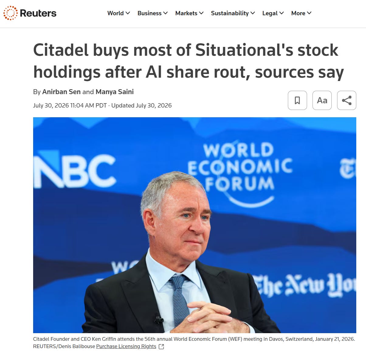
Amid the AI stock plunge, reports followed that prime brokers demanded margin-call-style collateral, and most of the public equity book was cleared in this deal [1][2]. That said, the fund itself was reportedly not liquidated. Assets shrank sharply from a recent peak of about $45 billion to somewhere around $10 billion, but the remaining $10 billion is reportedly centered on private holdings such as the Anthropic stake [3]. What got cleared, it seems, was the leveraged public equity side. The reported leverage was up to about 400% [1], and by the investor letter the one-month loss in July was about 67% (monthly, on a portfolio basis), yet even after taking that drawdown on top of a cumulative 439% in the first half, roughly plus 80% versus the start of the year remained, which is the strange scale of this event (from 5.4x, a July of minus 67% leaves roughly 1.8x, that is about plus 80%, so the arithmetic checks out) [4].
But when you actually open this fund’s Q1 2026 13F filed with the SEC [5], the picture looks more interesting.
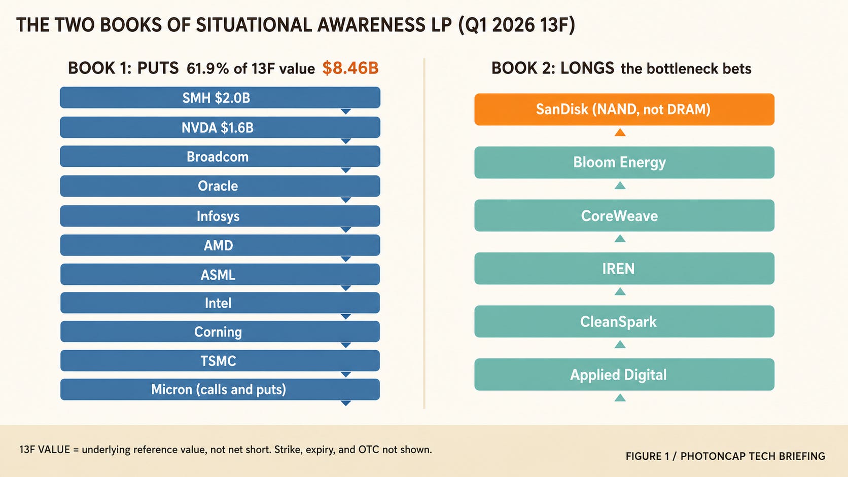
Figure 1: The Two Books of Situational Awareness LP, Q1 2026 13F
As is commonly known, this fund did not only buy semiconductor and AI infrastructure stocks. As of the end of Q1, the 13F reported value of the puts placed across the semiconductor and AI infrastructure stack was $8.46 billion, about 62% of the total reported value (roughly $13.68 billion). The semiconductor ETF $SMH at $2 billion, $NVDA at $1.6 billion, plus Broadcom, Oracle, Infosys, AMD, ASML, Intel, Corning, TSMC, and even Micron were on the put list [5][6].
One important caveat. The VALUE of a 13F option is not the option premium or a delta-adjusted net exposure but the reported value of the underlying security. So you must not read $8.46 billion as an actual P&L sensitivity or a net short size. On the other side, the axis of the longs was names like NAND flash SanDisk, a hot memory name of 2026 (over 1 million common shares plus added call options), Bloom Energy in power, CoreWeave, and IREN, CleanSpark, Applied Digital that pivoted from mining to AI hosting [6].
Here is a point I found a little interesting: the biggest memory name on the long side is SanDisk, and SanDisk’s current core business is not the DRAM or HBM that a GPU really needs but, somewhat unexpectedly, NAND flash storage. So the SNDK long can be a bet on the NAND and storage cycle (and on HBF, which comes later), but I do not think this position by itself proves a DRAM or HBM shortage. In this article, as in the title, I classify SNDK not as evidence for the memory long argument but as a somewhat separate, distinct position.
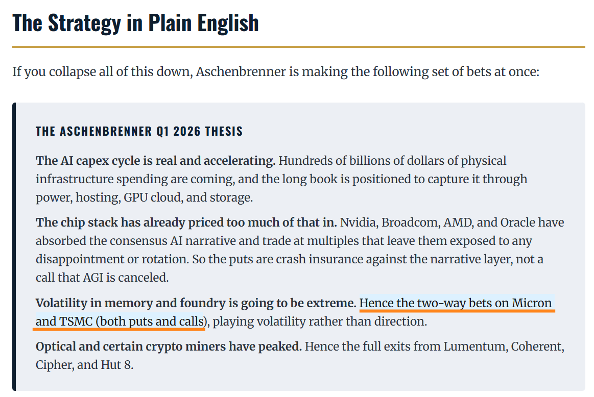
The original filing is not as clean as the title either. Micron, a US HBM player, has both calls and puts on it at once, so you cannot pin down which way it points, and TSMC, the representative foundry player, has both sides too [7].
The 13F distinguishes whether a position is a put or a call, but it does not show strike, expiry, premium, OTC derivatives, or stock shorts, so you cannot fix the fund’s net exposure from this document alone. Still, six tenths of the reported value is semiconductor and AI infrastructure puts, and the directional-long, bottleneck-side names were memory and power. It is a little unfortunate that for SK Hynix, with no US ADR as of the end of March, you cannot judge Korean-listed holdings from the 13F. In July reporting SK Hynix was mentioned as one of the fund’s major loss names, but the holding vehicle (Korean-listed share or ADR) and the timing of acquisition are not confirmed [8][9].
What is interesting is the side that, unlike SALP, survived this scene of extreme fear and is still holding the trade. In Atreides Management’s Gavin Baker’s latest 13F (as of March 31, 2026), Micron is among the top five holdings on a common-stock basis, and next to it sit connectivity-layer names like Ciena, Lumentum, Coherent, and Astera Labs [10]. Because these names are about “connectivity,” they are closely tied to optics, and I also see Lumentum and Coherent, which I like. That said, Atreides is not a pure-long-only book either. In the same filing an index put (QQQ) is actually the single largest reported position, so if you compare with one side’s hedges detailed and the other side’s longs highlighted, the basis becomes asymmetric [10].
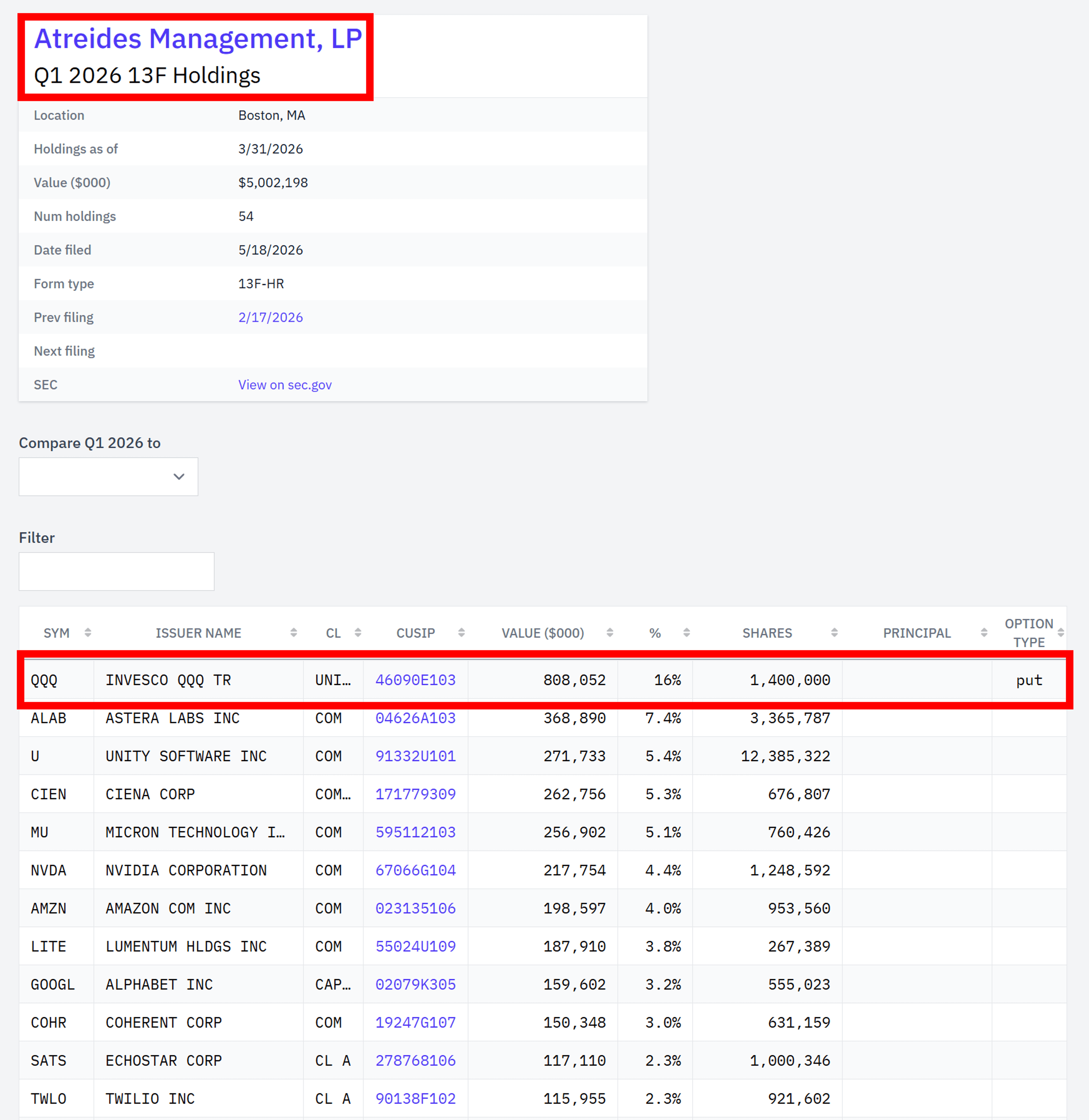
SanDisk, which was a strong long position in SALP, appears to be absent from this filing. SNDK is a 13(f) reportable security, but the absence of a reportable long in the end-of-March filing means only that holdings above the reporting threshold are not confirmed, not proof that the holding was zero. That is, a small holding or confidential treatment is possible. As for SK Hynix, there was no US ADR at the time, so you cannot judge Korean-listed holdings from the 13F. This point is a bit of a limit.
On the other hand, in Gavin’s case, from his remarks he publicly pointed out the valuation contradiction that semiconductor equipment stocks trade at roughly 40x next-quarter annualized earnings, while the memory produced through that equipment sits at a mid single-digit P/E [11], and while acknowledging that by the playbook of the past 25 years of memory cycles now is the time to sell, he still stands on the memory side (per summarized conference reporting) [12].
So this article I am writing today is not about “the two funds’ AI long positions.” It is about two different books (different names, sizes, and endings). Is the value of the AI stack moving from compute engines like CPUs and GPUs to the physical bottleneck? One side answered that question with heavy leverage and could not withstand the market’s volatility and decline [4], and the other side keeps the same question at a size it can hold.
I see the trade’s fate as likely decided by position structure and sizing more than direction. That said, net exposure, option terms, and per-position July P&L contribution are not disclosed, so I do not think you can conclude from the 13F alone that “the direction was right and only the size was wrong.”
So then, the two people, Leopold and Baker, why did they see compute as expensive and memory as cheap.
Situational Awareness’s 13F was a dual structure of semiconductor and AI infrastructure puts (reported value $8.46 billion, about 62%) and bottleneck longs, and Atreides’s filing has Micron and the connectivity layer side by side (though there is a QQQ put too). What the two funds share is not a position but a question.
2. Why Memory Sold Cheap for 30 Years
To answer this question, it seems best to first understand why memory was cheap in the first place. To help understanding, let me borrow flour, something we commonly encounter. DRAM is close to flour, and a GPU is, in a way, a premium ingredient handled in a Michelin restaurant kitchen. But it is not standardized.
By contrast, flour has a spec. If it is all-purpose grade 1, whatever mill’s product or brand it is, you generally get bread of the quality you expect. So the baker looks at price rather than the flour’s brand or label. DRAM is a product of a similarly designed market. Once a standards body called JEDEC sets a certain fixed spec for items like DDR5 and LPDDR5, then whether it is a chip made by Samsung or a Micron chip or an SK Hynix chip, among equivalent configurations that have passed JEDEC qualification the substitutability is very high. In other words, what matters is DRAM’s price.
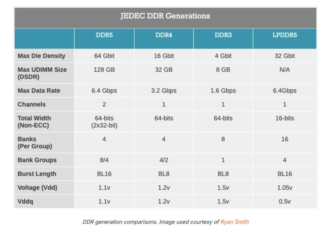
Of course, in a real system density, rank, timing, ECC, PMIC, thermal, and platform qualification (QVL) come into play, and a platform vendor like Intel also runs compatibility validation separately from JEDEC conformance [13]. Even so, commodity DRAM has a relatively low switching cost, so from the buyer’s standpoint there is little reason to weigh brand much, and they end up deliberating over the price tag.
And at the same time supply-side circumstances overlap here. As is well known, a memory fab takes years and tens of billions of dollars to build, but once built it is hard to stop. Because most of the cost is fixed, like depreciation, even in a downcycle it is reportedly better to print and sell one more wafer than to idle. So even if demand rolls over, supply does not, and price falls to near cash cost. Then when supply is cleaned up it becomes scarce again and price jumps, that so-called “cycle” repeated. An industry where price per bit has fallen for over 30 years, an industry where the next bust reclaims the boom’s profits. The market assigning memory a low multiple was precisely the result of learning.
But the Michelin kitchen is a completely different story. A Michelin chef’s dish is bound together with the recipe and the whole kitchen, so you cannot swap it out for the restaurant next door’s dish. What NVIDIA sells is also not a single chip but a system bound together with the CUDA software ecosystem, the developer base, and networking. When you cannot swap it in, that is exactly where pricing power arises. This is, to take a foundry example, how TSMC, holding an overwhelming lead in leading-edge foundry, has protected its margin by the same principle.
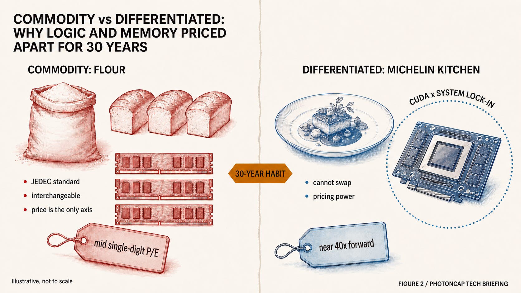
Figure 2: Commodity vs Differentiated: Why Logic and Memory Priced Apart for 30 Years
So the market developed a so-called “30-year” habit. A differentiation premium on logic, a commodity discount on memory. In other words, is not today’s gap that Baker pointed out, equipment at 40x versus memory in the single digits, the result of this habit [11]? That said, this P/E comparison may not be apples to apples because the target companies, GAAP versus non-GAAP, and forward basis differ, and the point that the moment memory’s P/E looks lowest may actually be the cycle peak is something I revisit later.
3. 2026, Cracks in the Price Structure
What the two funds, SALP and Baker, saw is probably the gap between this habit and reality. At some point flour prices started moving in a way that is not very flour-like.
By TrendForce’s tally, 3Q 2026 server DRAM contract prices are projected to rise 13 to 18% quarter over quarter, and this is called a “calming” phase, which is to say the prior quarters’ increases were even larger (over 90% in Q1, 50 to 60% in Q2) [14]. SK Hynix CEO Kwak Noh-jung, in an interview around the Nasdaq listing, said 2027 would be the worst year in industry history from a supply standpoint, and that excess demand could continue past 2030 [15]. In other words, it is now not a cyclical industry but structural shortage [16]. The stock price showed the same conclusion. SK Hynix’s Korean-listed share is up about plus 420% over the last 12 months, and even reflecting the pullback from the June peak it has risen nearly 8x (Korean-listed basis, as of 2026-07) [17].
At the center of this DRAM and memory price-structure change is that HBM we know well. HBM (High Bandwidth Memory) is memory that stacks DRAM dies vertically, connects them with through-silicon vias, and places them right next to a compute engine like a GPU, that is, the processor. But one misunderstanding needs to be cleared. HBM is also a JEDEC standard. HBM3 and HBM4 have spec documents too. The point where it diverges from flour is not the presence of a standard like JEDEC but exactly the switching cost.
Stacking method and yield, and thermal management and packaging differ by supplier, qualification with a customer’s chip takes several quarters, and it is sold not on spot but on multi-quarter long-term supply contracts. From the HBM4 generation, the share of advanced logic in the base die at the bottom of the stack grows and some of it goes custom (it differs by supplier and product, and Micron specifies an optional custom base logic die in HBM4E), so a differentiation layer is added. In short, HBM has higher customer-qualification and package-integration cost than commodity DRAM and a higher share of long-term contracts, making it a product where switching suppliers is hard. That is, it shows a character similar to the Michelin restaurant ingredient mentioned above. The path by which, as HBM demand grows, memory gets pushed out into a shared pool beyond the optical connection was covered in a previous article [18].
The market too started putting money on this change. On July 10, SK Hynix listed an ADR on Nasdaq and raised a large amount, one of the largest US listings by a foreign company, with subscription demand more than 7x the supply [19].
But in that very July, something in the exact opposite direction happened. In one month from the late-June peak, SanDisk, a NAND flash flagship, fell over 40%, the neocloud Nebius fell over 46%, and SK Hynix also slipped about 40% from its June peak [8]. In this situation one of the last triggers was China. CXMT, the number four in DRAM, jumped 466% on its first day on the Shanghai listing (over 500% intraday at one point, versus the IPO price) and became China’s most valuable listed company, but the fear that China-origin supply could end this crunch rode that symbolism and hit memory across the board [20].
The point I am curious about is how to interpret this July drawdown. Is this blow to memory across the board a disproof that “memory was flour after all”? Or is it old fear making one last cover in the transition from commodity to a contract-type asset.
To judge it you now have to look not at price but at physics. It is normal capitalist operation for substitutes to appear when a commodity gets expensive, so in memory what becomes a substitute and what does not. That answer is the floor of this whole trade, and the place where optical connection slots in is right there.
Below is the original text of Situational Awareness’s 13F filed on SEC EDGAR on May 18 [5].
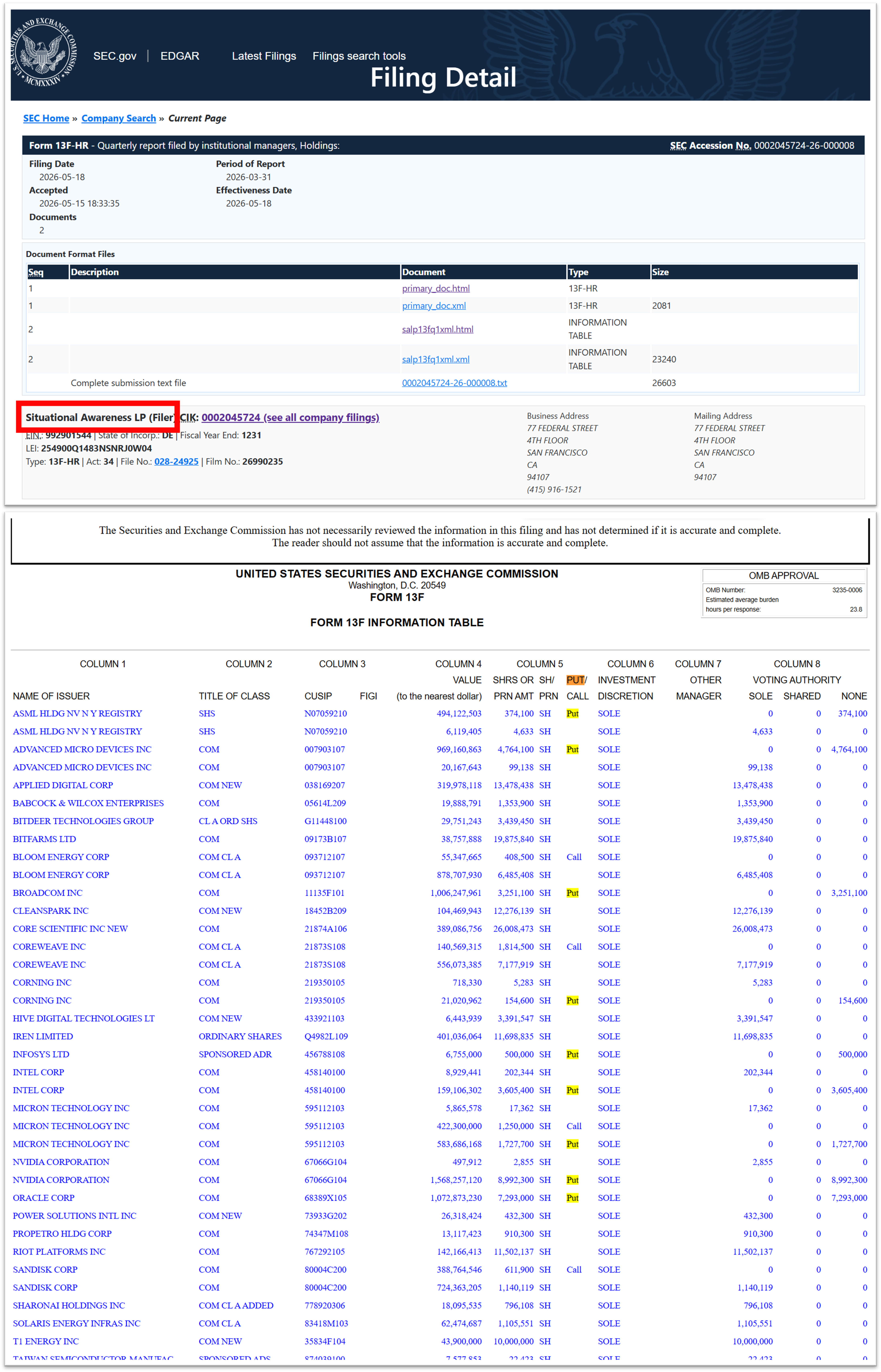
Figure 3: Screenshot asset: SEC EDGAR, Situational Awareness LP Form 13F-HR, filed 2026-05-18
HBM, even with a standard, has a high switching cost and is in effect memory sold on a contract basis. The contract-price rise and the July drawdown are two sides of that transition, and the criterion for judgment is not price but physics. (The 13F figures in this section are a March 31 snapshot and do not reproduce the pre-liquidation portfolio of July 30.)
4. What Can Replace DRAM
When prices rise like this, normally a substitute appears. But so far, exceptionally, in memory the force that tries to create a substitute has mostly been blocked by physical constraints, yet let me still look at the candidates.
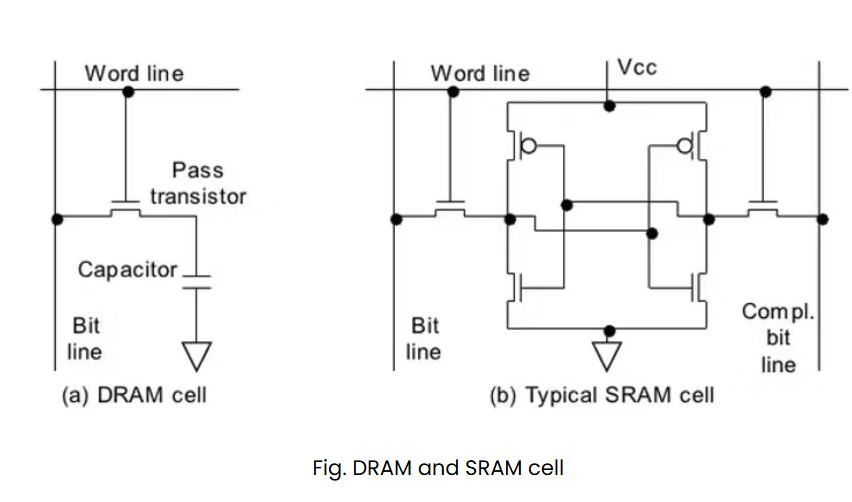
SRAM: the fastest but takes up too much room (the chip’s footprint). SRAM, used as cache inside the processor, is tens of times faster than DRAM. Told only this it sounds like a very good candidate, but the problem is that storing one bit needs 6T (six transistors). DRAM needs 1T1C (one transistor and one capacitor). The number of bits you can pack into the same physical area differs by an order of magnitude. On top of that, even in the latest logic process, SRAM’s cell area no longer shrinks well because of a fundamental physical constraint.
NAND (as pure flash): the cheapest with ample capacity, but too slow a candidate. Price per bit, NAND is overwhelmingly cheap. But its access time is on the order of microseconds. DRAM is on the order of tens of nanoseconds.
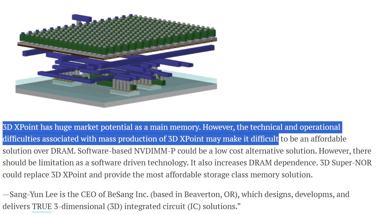
New memory: there have continually been attempts to insert a new layer between DRAM and NAND. Substitutes like PCM, MRAM, ReRAM were floated. The most serious attempt was Intel’s 3D XPoint Optane, but the ending was not good.
HBF (High Bandwidth Flash): SanDisk is emphasizing HBF, which raised bandwidth by giving NAND an HBM-style vertical-stacking interface. At the same time it signed a standardization agreement with SK Hynix [21]. The core claim is that at roughly a similar package height it aims to greatly increase capacity versus HBM (at a similar price band). That said, HBF is not a thing meant to chase DRAM’s ultra-low latency and speed, but an approach to fill inference’s capacity tier far more cheaply. So to put it precisely, it should be seen not as “a replacement for the DRAM cell” but as a candidate for “partial substitution of the HBM capacity burden,” and many take the view that, still at the standardization and development stage, you cannot confirm it as a commercial substitute. And there is an opinion that it has to use optics, and the structure of HBF and its point of contact with optical connection was covered more deeply in a previous article [22].
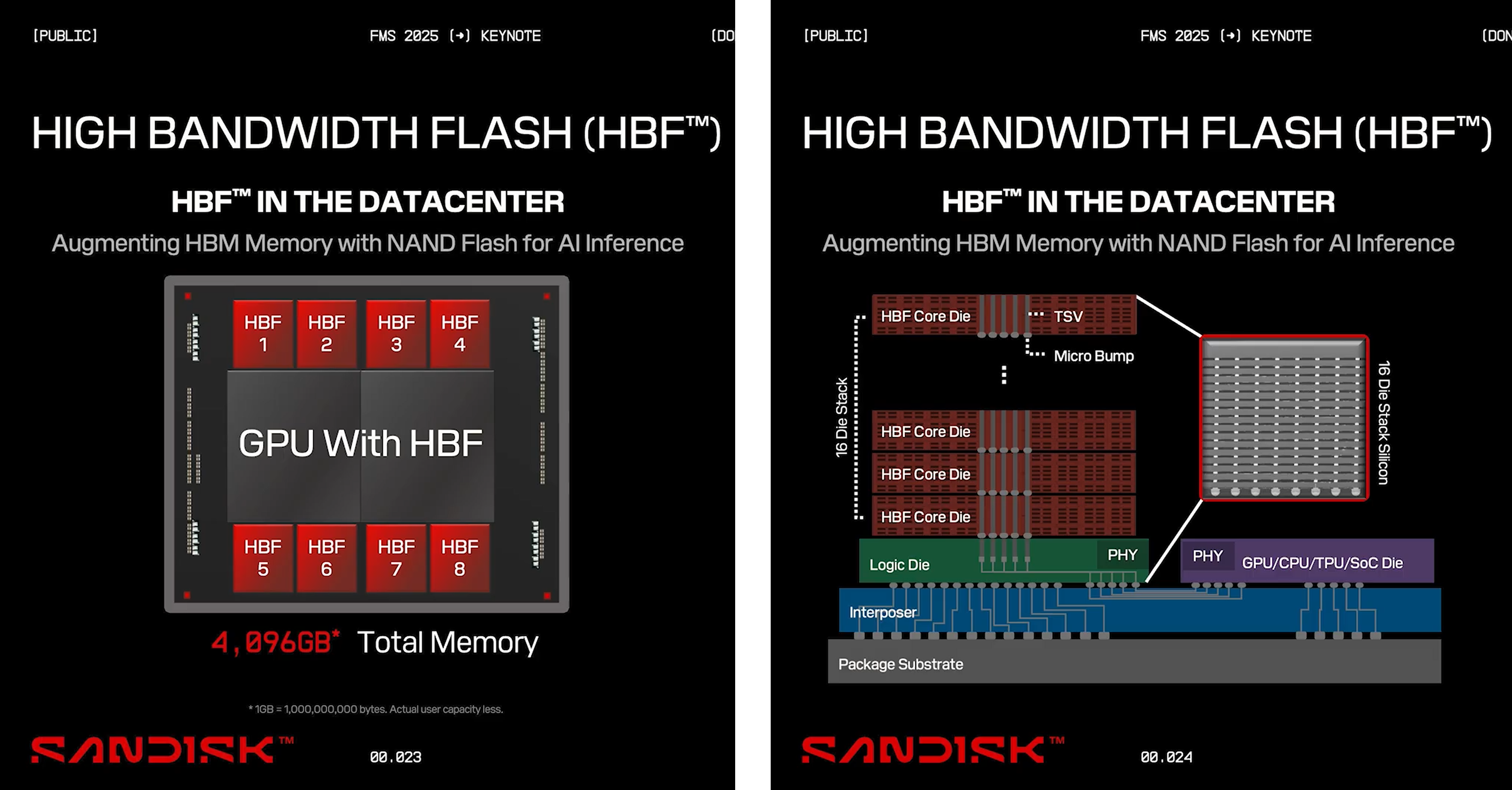
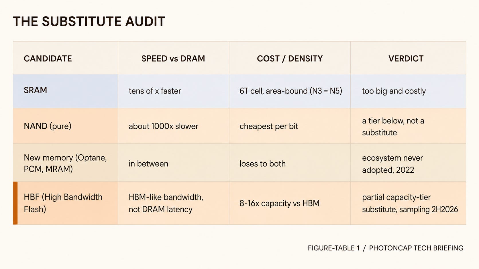
Figure-Table 1: The Substitute Audit: SRAM / NAND / New-Memory / HBF and Where Each Lands
So then, can you not just make more DRAM itself? Right here is the second physical wall.
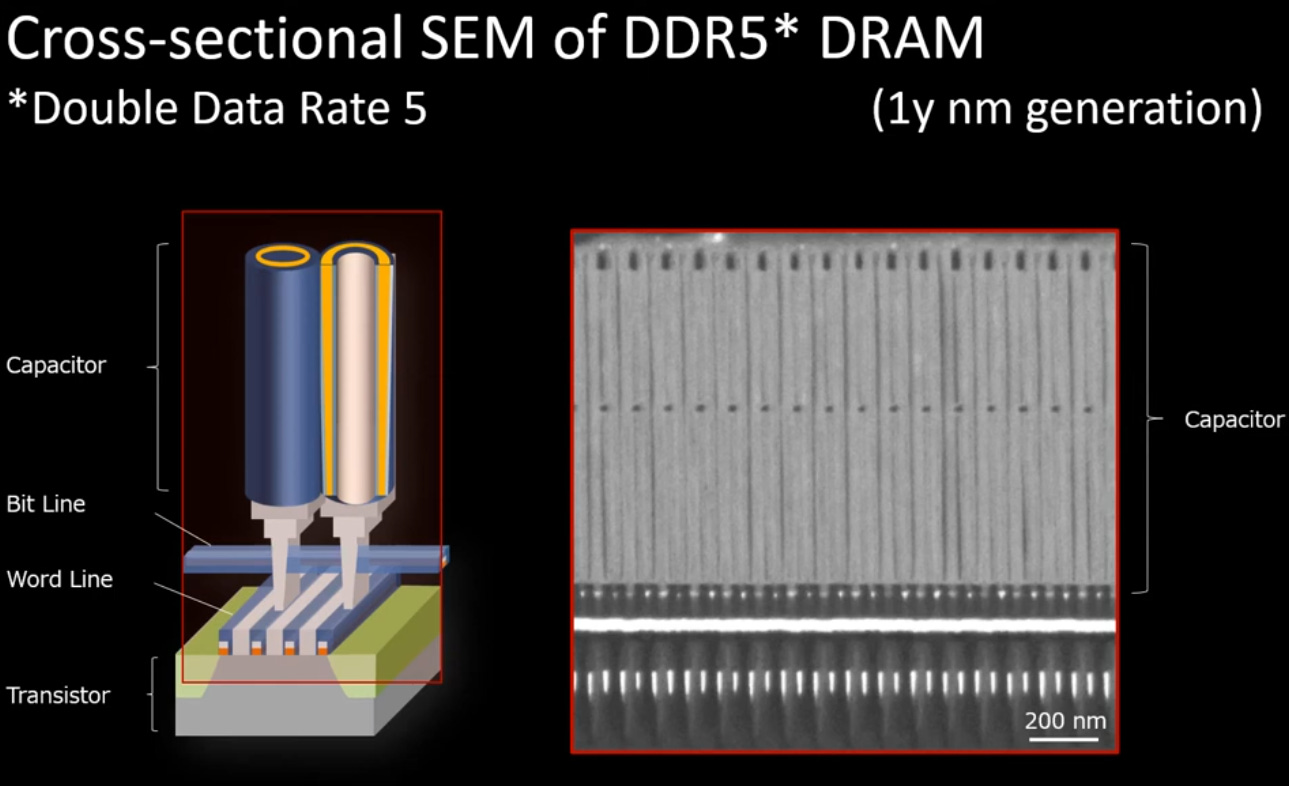
One bit of DRAM, as said above, consists of one transistor and one capacitor (1T1C). If you liken charge to water, the capacitor is the bucket that holds that charge. In process terms, this bucket is exactly the problem. If, because of area, you shrink it sideways, the charge it holds drops and reads become unstable from noise, so you have to pull it up long as much as you shrank the side (to keep total capacity). As a result, today’s DRAM capacitor is a pillar whose height is tens of times its width, and the aspect ratio is enormous.
And at the same time, the difficulty of erecting billions of these pillars identically rises every generation. Because it is not a structure where, like logic, shrinking the transistor automatically brings along performance and density, even bringing in advanced equipment like EUV, the efficiency converted into bit growth is not large compared to logic.
In fact the process-generation names testify to this stall. While logic goes down to 7nm, 5nm, 3nm, DRAM only swaps the suffixes 1a, 1b, 1c somewhere in the low 10nm range. That is, there was no big advance in the 10nm range.
Oh, of course, the effect of scaling has not vanished. Recent node transitions still have cases that give bit-density improvement of about 30 to 35% [23]. But the process complexity and cost to obtain that improvement have grown much larger than before, so it would be accurate to say that making economic bit growth as before has become hard.
On top of that, because the capacitor leaks charge, you have to refill it every tens of milliseconds (refresh), and as cells get smaller this maintenance burden grows too. So DRAM’s bit growth, once you subtract the contribution of process transition and yield improvement, comes largely from wafer input and capex. The point is there is no free growth of the kind scaling gives to logic.
As mentioned, DRAM is not easy to make, but that precious, costly wafer that should go to DRAM is now being used for HBM. HBM has large dies, the through-vias for stacking (TSV) take up area, and the yield after stacking several drops multiplicatively.
Micron has stated that, on a same-bit basis, HBM3E consumes about 3x the wafers of D5 [24]. Naturally, from a maker’s standpoint it is rational to allocate wafers first to high-margin HBM, and the more it does, commodity DRAM supply shrinks. As a result of this, it means this cannibalization is a big cause among the supply-side factors of the memory contract-price rise. This is something I see as physically unsolvable until new fabs are completed.
In conclusion, DRAM’s ultra-low-latency seat is still filled only by DRAM, and DRAM’s capacity expansion is possible only with time and money. In the capacity tier HBF has come up as a candidate to partially share the burden, but it is still at the development stage. Kwak Noh-jung’s “past 2030” remark is not exaggeration but a physical reason [15], and it is also the reason it fits when you read the two funds’ positions as memory being not a “chip seller” but a “bottleneck that is hard to expand.”
Key point: SRAM drops out on area, pure NAND on speed, new memory on ecosystem. HBF is an exception as a partial capacity-tier substitute candidate but is still at the development stage. DRAM capacitor physics makes economic bit growth hard, and HBM’s wafer cannibalization squeezes commodity supply.
5. What the Bottleneck Really Is: Not Capacity but Access Speed
Now then, the word bottleneck needs to be made one layer more precise.
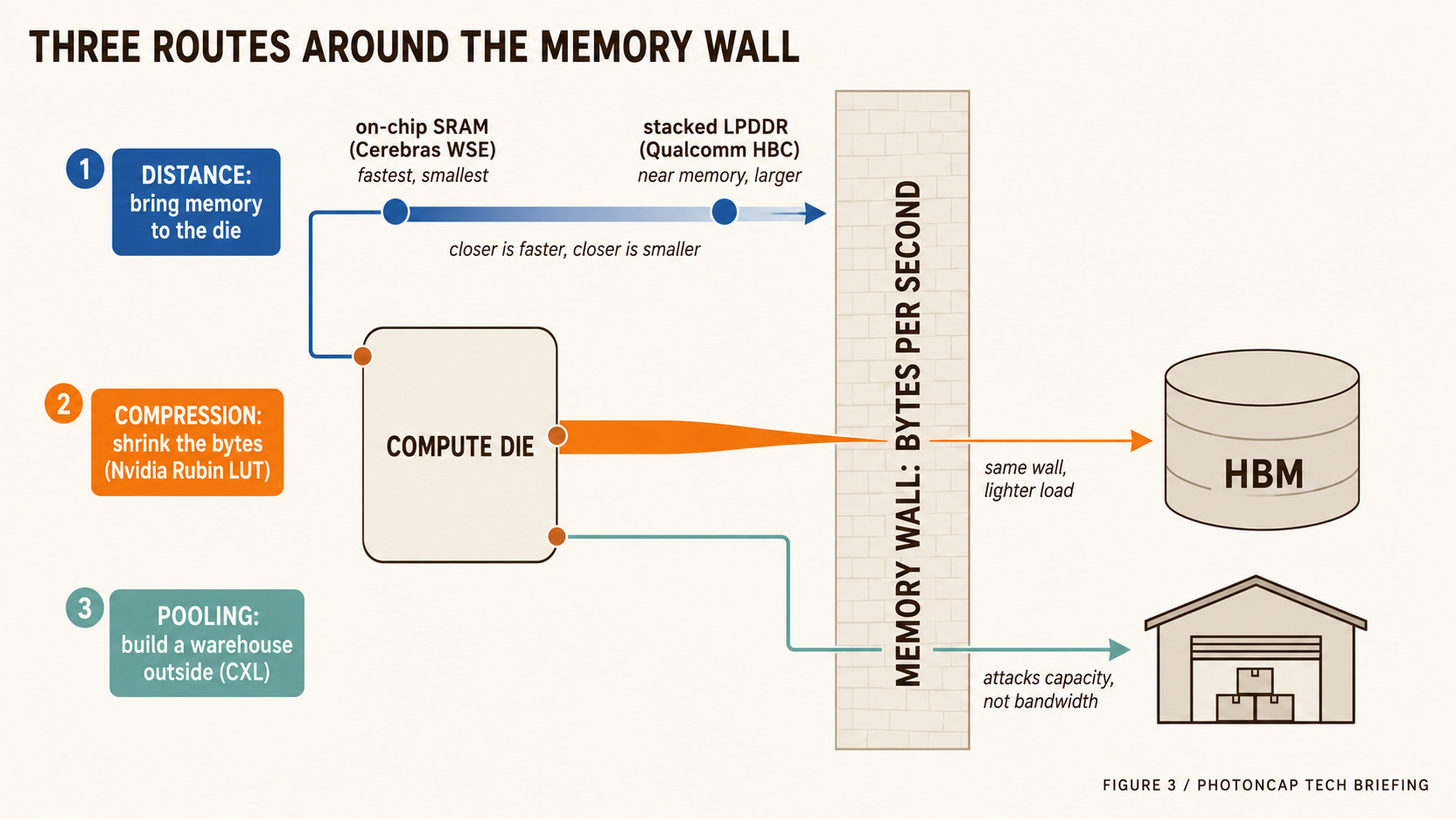
In fact the bottleneck is not one but two. One is the speed at which a compute engine like a GPU reaches local HBM (the bandwidth wall), the other is the total memory to hold the model and the KV cache and rack-level utilization (the capacity and utilization wall). This is a thesis I have repeated in this article, and a piece I wrote recently: the three-branch approach to bypassing the memory wall was laid out in detail in a previous article [25].
In the decode phase where an LLM generates the answer one token at a time, each time it makes one token it has to read the model weights and the KV cache heavily. In a single request or low-batch dense decode the per-token throughput limit is set roughly by “memory bandwidth divided by bytes read per token,” so the GPU’s compute engine idles and memory bandwidth sets the schedule. (Bandwidth is limited, but because bytes read per token grow, speed drops and accordingly a situation arises where compute engines like GPUs idle.)
So then, what about not low-batch dense decode but when the batch grows?
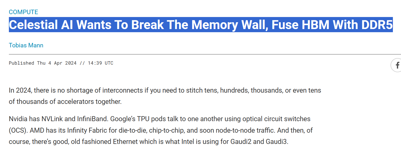
Weight reads are amortized across many requests, and depending on MoE, quantization, speculative decoding, attention structure, and context length, I see the bottleneck able to move to compute, capacity, or interconnect. So “bandwidth is unconditionally the only bottleneck” is not the case, and it is especially so under low-batch conditions. To borrow the phrasing of Celestial AI founder Dave Lazovsky, the industry right now is using NVIDIA GPUs as “the most expensive memory controllers in the world” [26]. I also agree with this.
If you accept this diagnosis, compute puts and memory longs are not two different bets but read as two sides of a fundamental constraint by the same system, or of that diagnosis. It is a diagnosis that on the non-bottleneck side (compute) the price carries a bottleneck premium, and on the bottleneck side (memory) the price carries a commodity discount. That is, put differently, the fact that the real bottleneck memory carries a discount rather than the premium it ought to receive, and that compute has a premium, is what Leopold’s book and Baker’s remarks come close to as a structure.
The next variable after this diagnosis is the wiring. If access speed is the bottleneck, where does the technology that changes the wiring itself stand? Right here is the point where optics enters.
6. Where Optics Slots In: The Technology That Moves Memory
Coming back to filings again, in Situational Awareness’s Q4 2025 book there was the optical component company Lumentum, but in Q1 it was fully sold along with Coherent [7]. The reason for the sale is unfortunately not knowable from the filing alone. Valuation burden, risk reduction, hedge adjustment against another position, many readings are possible, and the only certain thing is the fact of the sale.
By contrast, in Atreides’s latest filing, next to Micron, Ciena, Lumentum, Coherent, and Astera Labs still sit side by side [10]. In short, the 13F does not neatly tell the story that “the bottleneck fund holds optics.”
Because optical connection has to be derived not from filings but from technical analysis, from here I try to move not to positions but to a physical story.
An electric link carried over copper, as frequency rises, has channel loss growing sharply as bandwidth and distance grow together, and the equalization and retimer power to correct it swell quickly. There is thermal loss too, of course. This is why an HBM-class-bandwidth interface sits inside the same package as the processor, at millimeter distance.
As a result, the ratio of memory capacity to bandwidth loaded on a single GPU is fixed at packaging time. If you need more memory, the structure is that you have to buy a whole new GPU with compute attached. What Lazovsky’s “most expensive memory controller” line points to seems to be this fixed ratio [26].
But unlike copper, light has this distance constraint much looser.
Optical connection, even crossing meters, has small loss and power penalty versus electric, so in theory you can pull memory out of the package, even into a separate chassis, and make a pool shared by multiple processors. It is not a technology that replaces memory but a new-paradigm technology that changes where memory sits. How this optical memory fabric got tangled with actual stock flows (the SOCAMM selloff and so on) was covered in a previous article [27].
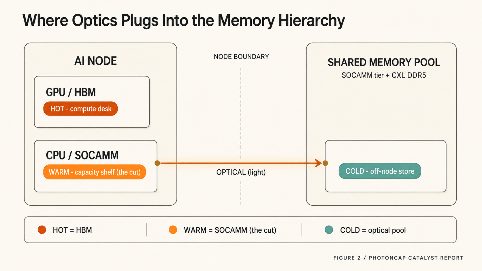
That said, I want to stress that this deals mainly with the capacity and utilization wall and data movement among the two walls divided above, but is not a technology that directly replaces or copies the fundamental problem, local HBM’s latency and bandwidth.
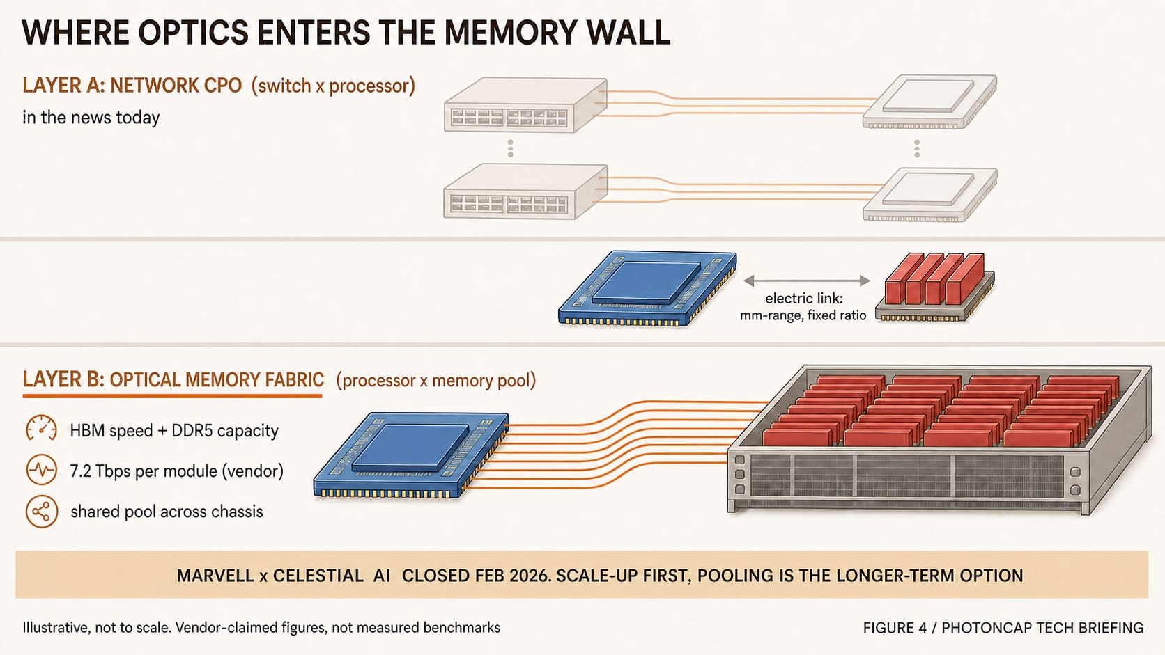
Figure 4: Where Optics Enters the Memory Wall: Network CPO vs Optical Memory Fabric
The company trying to commercialize this inner layer head-on is Celestial AI. At OFC 2025 it presented an architecture implementing memory-compute disaggregation with an optical fabric [28], and module specs are public too. Two HBM3e stacks act as a cache for large-capacity DDR5 so the processor sees HBM’s speed and DDR5’s capacity at once, connected at 7.2 Tbps optical bandwidth per module, and by bundling several such modules it builds a shared memory appliance in the tens of TB range [29].
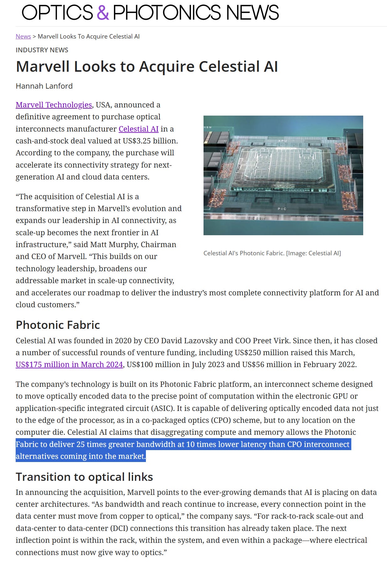
Marvell announced the acquisition of this company in December 2025 and completed it on February 2, 2026 (about $3.25 billion) [30]. So then, why did Marvell acquire such an optical connection company?
The first commercial application Marvell put forward is not pooled memory but all-optical scale-up interconnect, and the meaningful revenue-contribution timing was guided to the second half of FY2028 (from a $500 million annualized run rate per quarter, doubling thereafter) [30]. That is, optical memory pooling can be read as not the center of the current business but an option on a longer horizon. Seeing $MRVL right now as immediately “optical memory pooling” seems a bit not easy. The vendor-claimed figures of “25x bandwidth and one tenth the latency versus prior CPO” are worth keeping an eye on [31].
From a memory maker’s standpoint, how does the direction of this optical connection technology look?
Even if memory goes out to the shared pool beyond the optical fabric, what fills that pool is still the same three makers’ DRAM, so it ends up raising total DRAM bit demand. At the same time pooling can reduce stranded HBM and raise utilization, playing the role of lowering the total of costly local HBM that must be mounted per accelerator. In some workloads DDR5 or, later, HBF could take a larger share instead of local HBM.
So in the investment picture the position sorts out like this. If the memory long is a bet that “the bottleneck should get expensive,” the optical memory fabric is, I think, a longer-horizon bet that “a premium attaches to the connection that unblocks the bottleneck.”
It got long, so to sort a little: “optical connection is not a technology that replaces memory but one that breaks the fixed ratio of processor to memory and moves memory into a shared pool.” “Marvell’s Celestial acquisition closed in February 2026, the first market is scale-up, memory pooling is the longer option.” That is it.
References & Sources
[1] “AI investor Leopold Aschenbrenner forced to unwind all public stock positions after steep losses, sources say”, CNBC, 2026-07-30
[2] “Citadel buys most of Situational’s stock holdings after AI share rout, sources say”, Reuters, 2026-07-30
[3] “Situational Awareness Drops to $10 Billion on Citadel Pact”, Bloomberg, 2026-07-30
[4] “Situational Awareness’ portfolio sinks 67% in July on AI stock rout, letter shows”, Reuters, 2026-07-31
[5] “Situational Awareness LP, Form 13F-HR, Period 2026-03-31”, SEC EDGAR, filed 2026-05-18
[6] “Leopold Aschenbrenner’s ‘Situational Awareness’ Files 13F Quarterly Investment Disclosure”, Yahoo Finance, 2026-05-18 (secondary summary)
[7] “The Most-Anticipated 13F of 2026: What Leopold Aschenbrenner Actually Owns”, DaveManuel.com, 2026-05-19 (secondary)
[8] “NVDA, NBIS, SKHY, SNDK Stock Losses Reportedly Force Ex-OpenAI Researcher’s $20B Fund To Seek Capital”, Yahoo Finance / Stocktwits, 2026-07-30 (secondary)
[9] “SK Hynix Stock Jumps 14% on Nasdaq Listing”, INDmoney, 2026-07-10 (secondary)
[10] Atreides Management, LP: Form 13F-HR, Period 2026-03-31 (54 holdings; INVESCO QQQ put is the single largest reported position, Micron 760k common shares), SEC EDGAR / 13f.info (accession 0001777813-26-000006), filed 2026-05-18
[11] “15 Key Takeaways From Gavin Baker’s Invest Like the Best 2026 Interview”, Global Data Center Hub, 2026-06-02 (interview summary)
[12] “Sohn New York 2026: Baker and Khaira on the Shortage That Could Save AI From a Bubble”, Hedge Fund Alpha (2026 Sohn NY, Gavin Baker x Jas Khaira fireside; “based on every memory cycle over the past 25 years, now is 100% the time to sell”)
[13] “Intel Memory Validation Results”, Intel (basis for separate platform validation)
[14] “Server DRAM Contract Prices Expected to Rise 13-18% QoQ in 3Q26, Says TrendForce”, TrendForce, 2026-07-09
[15] “SK Hynix CEO Expects Memory Crunch to Last Beyond 2030”, Bloomberg, 2026-07-10
[16] “SK Hynix CEO Sees Worst-Ever Memory Supply Shortage in 2027, Says Demand to Outstrip Supply Beyond 2030”, Reuters via U.S. News, 2026-07-10
[17] “SK Hynix stock’s US listing could signal whether the market can still boom…”, Fortune, 2026-07-05
[18] PhotonCap, “The More Anthropic Buys Micron HBM, the Faster Optical Memory Pooling Arrives”, 2026-06-24 (PhotonCap self-citation)
[19] “SK hynix US listing more than seven times oversubscribed, source says”, Reuters, 2026-07-09
[20] “Chipmaker CXMT’s 466% market debut surge makes it the most valuable China-listed company”, CNBC, 2026-07-27
[21] “Sandisk and SK hynix join forces to standardize High Bandwidth Flash memory, a NAND-based alternative to HBM for AI GPUs”, Tom’s Hardware, 2025-08 (HBF standardization MoU, 8 to 16x capacity, samples 2H 2026)
[22] PhotonCap, “HBF (High Bandwidth Flash) and Optics: The Missing Link in AI Infrastructure”, 2026-01-26 (PhotonCap self-citation)
[23] “How DRAM Changed the World”, Micron (context for node-transition bit-density improvement)
[24] “HBM is Coming for Your PC’s RAM: HBM consumes around three times the wafer capacity of DDR5 per gigabyte”, Tom’s Hardware (citing Micron remarks, HBM3E about 3x wafers)
[25] PhotonCap, “Three Routes Around the Memory Wall: Qualcomm’s Stack, Nvidia’s 3 Bits, and What Remains”, 2026-07-26 (PhotonCap self-citation)
[26] “Celestial AI Wants To Break The Memory Wall, Fuse HBM With DDR5”, The Next Platform (original Lazovsky interview)
[27] PhotonCap, “The Cut Was Not HBM: The SOCAMM Selloff and the Optical Memory Fabric”, 2026-06-16 (PhotonCap self-citation)
[28] “Photonic Fabric for Memory and Compute Disaggregation”, OFC 2025 Technical Digest, paper W3D.1
[29] “Marvell bets big on optical I/O with $3.25B Celestial AI deal”, Gazettabyte, 2025-12 (spec at announcement)
[30] “Marvell Completes Acquisition of Celestial AI”, Marvell, 2026-02-02 (acquisition closed, scale-up first, second-half FY2028 revenue guidance)
[31] “Marvell Looks to Acquire Celestial AI”, Optics & Photonics News, 2025-12 (25x / one tenth are vendor claims)
Additional read:

Disclaimer: This article is an independent, engineering-driven technical analysis published by PhotonCap. All content is based on publicly available information and is intended for educational and informational purposes only. Nothing herein constitutes a recommendation to buy, sell, or hold any security. The author may hold positions in securities discussed and may transact at any time without notice. Readers should conduct their own due diligence before making any investment decisions.
Is there a path where eventually Micron adapts its high-density Hafnium-Zirconium-Oxide (HZO) FeRAM architecture to work with Aeluma to accommodate cell-level optical modulators.
The resulting architecture could solve the active fiber alignment bottlenecks inherent in traditional Co-Packaged Optics, potentially enabling high packaging throughput at scale.
Or does Micron's existing reliance on TSMC and NVIDIA for external silicon photonics interposers connected via TSVs to HBM4 sufficiently address near-term memory wall bottlenecks without the yield risks of novel cell-level optical architectures for the foreseeable future?
Perhaps eventually scenarios like POET for future heterogeneous 3D integration on a base die or even IN the base die if sufficient qualification metrics are achievable...
As we've seen Apple was lobbying Trump admin. to allow its iPhones sold out of America to use CXMT memory chips, could CXMT pose a threat against those 3 big memory vendors due to its low prices?