
The Cut Was Not HBM: The SOCAMM Selloff and the Optical Memory Fabric
$MU $NVDA $MRVL | The CPU-side capacity tier bottleneck and the optical memory fabric

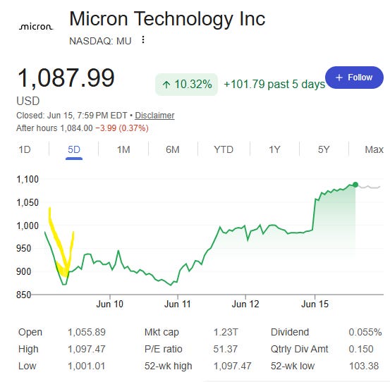
Micron fell close to double digits in a single session and the whole AI memory trade wobbled with it. The spark was a Dylan Patel note saying NVIDIA’s Rubin platform would halve its SOCAMM memory capacity, and the market read it as a sign that the memory cycle was rolling over. But the reported cut was on the CPU-side LPDDR5X, while the GPU-side HBM4 stayed untouched. The claim of this piece is simple. If the cut is real, it is less a sign of demand destruction than a sign that the local capacity tier is running into supply, power, and heat, and one of the most structural ways to relieve that wall is an optical memory fabric. Local DDR5 access is about 115 ns while an electrical CXL memory pool sits at 200 to 300 ns, and that gap is exactly where optics enters. We frame this around $MU, $NVDA, and $MRVL.
Contents
The Day It Broke
Which Memory Got Cut
Why It Got Cut: Supply, Not Demand
So Here Is the Real Question
Splitting the Memory Hierarchy by Temperature
Then Why Not Just Grow to 256 GB SOCAMM2
The Electrical Ceiling of CXL Is the Doorway for Optics
The Same Vector That Made SOCAMM Leads to Optics
Which Workloads Move to Light
Who Stands Where in the Supply Chain
Scenarios and Monitoring
What Would Make Me Drop This Thesis
Closing
The Day It Broke
Memory names cracked in a single session. Micron ($MU) dropped close to 10 percent intraday at one point, falling hard from near the prior day’s highs. SanDisk, Western Digital, and Seagate were dragged down with it. [1]
The trigger was a SemiAnalysis note that circulated on the morning of June 4, 2026. The content was this. NVIDIA could cut the CPU-side SOCAMM DRAM in the next-generation Rubin NVL72 rack from about 55 TB to about 28 TB per rack, roughly a halving. In module terms, the estimate was that the standard 192 GB configuration would drop to 96 GB, with high capacity left only as a custom option. [1][2]
That is where the market reflex kicked in. “Memory demand is cut in half, this is bad for Micron.” The price moved on that read. But the question is not whether the fear is real. It is whether the fear points the right way.
And this pattern looked familiar. Just days earlier, in the CPO selloff, the trigger was again a single line from a SemiAnalysis note, and the market read it as “CPO is dead” and threw every optical name into one basket. Yet many of the names that got sold were not even tied to CPO. The lesson I drew there applies here too. You do not look at one form factor or one BOM line, you look at which layer underneath is actually constrained on supply. SOCAMM is a BOM line. The layer that is actually constrained sits somewhere else.
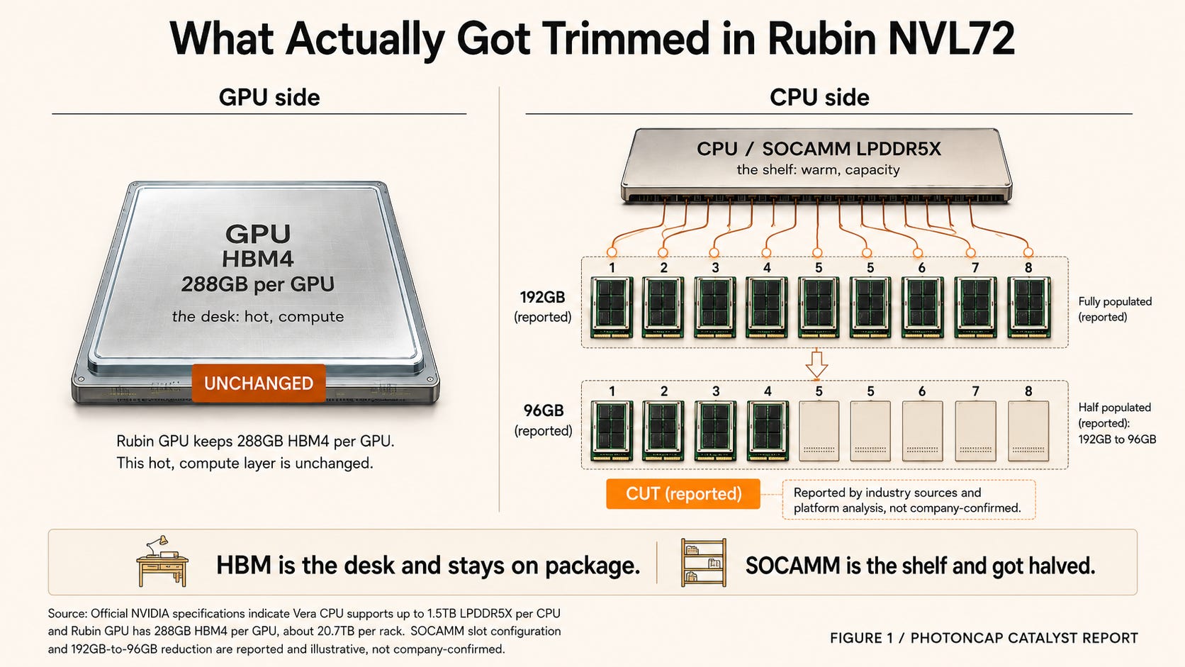
[Figure 1: What actually got trimmed. HBM is the desk and stays on package, SOCAMM is the shelf and got halved]
Which Memory Got Cut
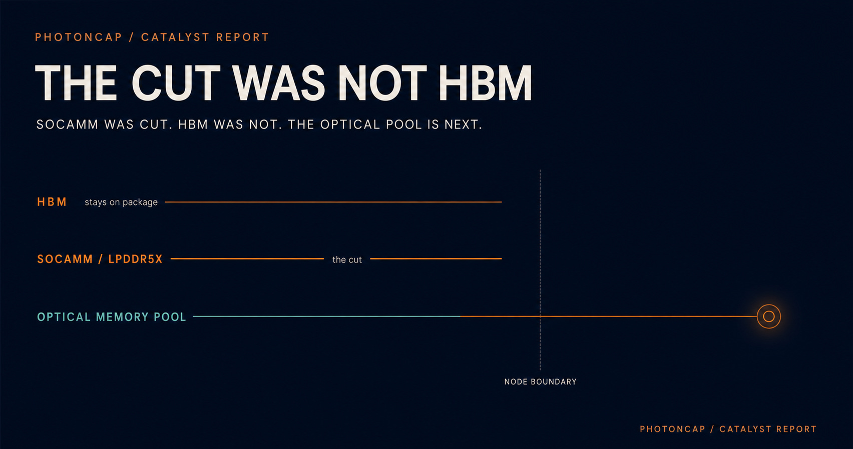
Start with an analogy. Think of a desk and a shelf. The HBM next to the GPU is the desktop. It holds the data you are computing on right now, so it is fast but expensive and small. The SOCAMM next to the CPU is the shelf beside the desk. You do not open it constantly, but it carries the capacity. This cut left the desk alone and trimmed only the shelf. The market read it as “memory overall got cut.”
Look at Rubin NVL72 from a memory angle and it is two blocks. The GPU side carries HBM4. That was not touched. On NVIDIA’s official spec, HBM4 stays at 288 GB per GPU and about 20.7 TB per rack. This is the layer where model weights, the KV cache, and training throughput live. NVIDIA itself describes LPDDR5X and HBM4 as one coherent pool, with the HBM KV-cache offloaded to LPDDR. [3]
The side that got cut is the CPU side. On NVIDIA’s official spec, the Vera CPU carries up to 1.5 TB of LPDDR5X, which works out to about 54 TB across an NVL72 rack of 36 Vera CPUs. Reports and platform analysis read that as eight SOCAMM slots populated with 192 GB modules. The cut scenario circulating in the market is the story of taking that 192 GB down to 96 GB. [3][2]
So what broke was not the high-bandwidth memory next to the GPU, it was the system memory next to the CPU. SOCAMM, the Small Outline Compression Attached Memory Module, is an LPDDR5X module form factor that NVIDIA built together with Micron, Samsung, and SK Hynix. The key point is that it is LPDDR5X, but in a socketed module rather than soldered down. At 14 by 90 mm it is about a third the size of a traditional RDIMM, and each module stacks four LPDDR5X stacks across 16 die. [4][5]
Capacity varies by generation and die density. The first generation was introduced around 128 GB, the SOCAMM2 generation moved to 192 GB, and Micron pushed it to 256 GB using a 32 Gb monolithic 1-gamma die. Eight 256 GB modules give 2 TB per CPU. Micron positions this high-capacity SOCAMM2 directly for offloading the KV cache from HBM to LPDDR. The heart of this cut is that the high-capacity 192 GB standard configuration can be lowered to 96 GB. [6]
The numbers make the meaning of the cut clear. On a reported basis of eight SOCAMM slots per CPU, the total LPDDR5X per CPU splits by module capacity like this.
96 GB x 8 = 768 GB per CPU 192 GB x 8 = 1.5 TB per CPU 256 GB x 8 = 2 TB per CPU
Going from about 54 TB on the official spec (the 192 GB configuration) to about 28 TB in the reported scenario (the 96 GB configuration), this cut is less “use less memory” and more a decision to ration the per-rack warm capacity tier by nearly half. HBM (about 20.7 TB per rack) is left alone and only the CPU-side capacity tier is adjusted. The reason the title reads “The Cut Was Not HBM” is in these numbers. [3][2]
Why does this module structure matter? Because it explains that the cut is the reversible kind. The contact pads run up to 694 versus roughly 260 pins on a DDR5 RDIMM, and that I/O density lifts the aggregate bandwidth per module. It operates at about 1.05 V, cutting memory power by 30 to 35 percent versus a DDR5 RDIMM. The design intent is to move the same capacity at lower power. Because it is socketed, you can install 96 GB now and swap to 192 GB later. That modularity was exactly what NVIDIA stressed at CES. Compute tray assembly time dropped from two hours to five minutes. “Install first, fill later” is built into the form factor. [5]
Why It Got Cut: Supply, Not Demand
This is the spot the market missed. If the public reporting and the supply-chain estimates hold, the more direct reason for the cut is high-capacity LPDDR5X supply and cost constraints rather than weakening demand. Along the TrendForce line, the 2027 preliminary allocation plans from Samsung, SK Hynix, and Micron cover only about 60 percent of the low-power DRAM NVIDIA needs. So NVIDIA chose to lower per-module capacity while raising total module shipments. Deploy more Vera CPUs, but size the per-module capacity to the supply ceiling. [7]
And SOCAMM is a form factor that died once and came back. The first-generation SOCAMM effectively folded on the GB300 “Cordelia” platform because it could not stay inside the thermal envelope. Socketed seating is worse than soldering for the heat path, and stuffing high-density LPDDR5X modules into the tight thermal budget next to the GPU hit the wall. What came out of that is the JEDEC-standardized SOCAMM2 (JESD328), which raises speed from 8533 to 9600 MT/s and adds SPD profiles. [8]
One more point. People lump everything together as “the DRAM shortage,” but in reality three branches compete for the same wafer. The HBM that attaches to the GPU, the LPDDR5X that smartphones and AI servers share, and the commodity DDR5 for servers and PCs. HBM eats a lot of wafer area per bit, so as HBM grows it squeezes the other two branches. SOCAMM uses the middle one, LPDDR5X, and because AI servers compete with smartphones for the same pool, 2027 gets especially tight. So reading this cut as “falling DDR5 demand” confuses the branches. What got cut is the LPDDR5X side, and it got cut because it is scarce, not because it is in surplus. Memory takes a large share of server power, so this capacity tier also gets heavier on power and cost the more you grow it. [9][7]
To put it plainly. The local capacity tier is being pressed from three directions at once. Supply (LPDDR5X scarcity), power (memory as a large share of server power), and heat (Cordelia overheating). The SOCAMM cut is the first visible symptom of that pressure.
Three things the market confused in this SOCAMM cut.
One. HBM did not get cut. The HBM4 next to the GPU is untouched, and what got cut is the LPDDR5X capacity tier next to the CPU.
Two. Memory demand did not vanish. If anything, high-capacity LPDDR5X supply is short, so the move is to lower per-module capacity and raise the number of systems.
Three. It does not mean an optical memory fabric replaces SOCAMM tomorrow. The local capacity tier hit the wall of supply, power, and heat, and one of the long-run ways through that wall is pooled memory and optical reach extension.
So Here Is the Real Question
This far is the range you can follow from public material. What SOCAMM is, why it got cut, why HBM was left alone.
Go one step deeper and a different picture shows up. If the local capacity tier is blocked by supply, power, and heat at the same time, then there is a ceiling on the very approach of packing more memory into each node. Replicating the same DRAM across every node gets more expensive and hotter the more you do it.
There are several paths through that ceiling. Larger SOCAMM2 (256 GB samples already exist), better LPDDR supply, CXL local expansion, software tiering, an NVMe and SSD tier, and memory compression all move together. One of the most structural among them is pulling memory out of the node, sharing it as a pool, and reaching that pool with light. And that overlaps with the optical layer PhotonCap tracks. [6]
Here is where the questions split. Does optics replace the tier SOCAMM holds, or extend it? Why is the CXL protocol not enough over copper, and why does it need light? In the same DRAM-short environment, why might the short-term price reaction of the three memory makers and the long-term thesis for the optical fabric read in different directions? And in this transition, who is actually buying up the pieces?
The answer is in the numbers. Local DDR5 is about 115 ns, an electrical CXL pool is 200 to 300 ns. That gap is the doorway for optics. The paid section works through who sits on which layer between that 115 ns and 200 to 300 ns, why Marvell is gathering Celestial AI and XConn as bets in the same direction, and how this picture could be wrong. Below we unpack the three-tier memory hierarchy, the supply-chain positioning, the scenarios, and the falsification conditions.
