
Abstract
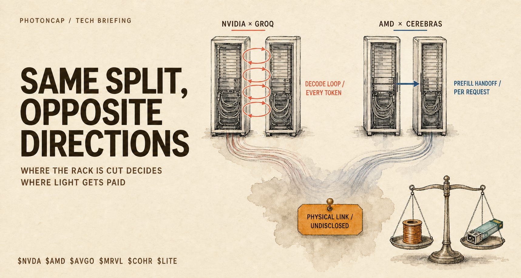
NVIDIA cut inside the decode loop. AMD and Cerebras cut between prefill and decode. $NVDA’s own documentation says the Rubin GPU and the LPX rack trade intermediate values on every output token, while $AMD and Cerebras have disclosed nothing about how data moves between their two machines, or over what physical link. Both carry the same label, inference disaggregation. But change where and how often that data moves, and the split of revenue between copper, plug-in optical modules, and switch-integrated CPO changes with it. This piece sorts the disclosed connection specs from the blank spaces, grades the evidence, and narrows down which disclosures would change the exposure of $COHR $LITE $MRVL $AVGO, and in which direction. My conclusion is one notch narrower than “optics wins either way.” The total volume of optics probably grows. Whether that revenue lands in modules, external lasers, CPO optical engines, or switch silicon is decided by where, on each link, light gets created and turned back into electricity.
Contents
NVIDIA in December, AMD in July
Why One Rack Isn’t Enough
They Wrote Down Everything Except the Wire
AMD’s 2 Pieces + NVIDIA’s 5
Once per Request, Once per Token
Inside the Rack: Copper This Far
Outside the Rack: Which Kind of Light
Not the Link, the Ends of the Link
Where Copper Steps Back
Scenarios and Monitoring
References & Sources
1. NVIDIA in December, AMD in July
NVIDIA’s Groq 3 LPX rack is designed to trade data with the GPU rack next to it every time it produces an output token[1]. AMD and Cerebras split prompt processing and token generation across two entirely different machines[2]. Both camps carved inference into two engines, but they carved in different places, and while NVIDIA’s documents spell out the rhythm of the exchange, AMD’s disclose nothing about the movement at all. The problem: neither company has said what actually connects those racks.
The timeline runs like this. On December 24, 2025, NVIDIA signed a non-exclusive inference technology license with Groq and brought over key personnel including the founder[3]. Neither company disclosed a price; CNBC, citing an investor, reported roughly $20B in cash[4]. Three months later at GTC 2026, NVIDIA unveiled the Groq 3 LPU as the seventh chip of the Vera Rubin platform, presented in a configuration where an LPX rack carrying 256 of these LPUs sits right beside NVL72[1].
Seven months after the license, on July 23, 2026, AMD delivered its answer in the same direction at Advancing AI 2026: a partnership that pairs Helios racks with Cerebras’s wafer-scale chip for ultra-low-latency inference[2]. Two companies that sell GPUs, roughly seven months apart, both put a crack in the same premise, that one kind of GPU rack handles all of inference best.
Not a coincidence. Behind both announcements sits the nature of the inference workload itself. And inside the difference between them, where each camp cuts the rack, sits the question of which segment of optical component demand shows up over the next few years. Why the same split points in opposite directions is the subject of this piece.
2. Why One Rack Isn’t Enough
An AI model produces an answer in two phases. Reading and understanding the question and its context from start to finish is prefill. Generating the answer one word at a time on top of that understanding is decode.
In restaurant terms, prefill is reading the whole order ticket and the recipe at once, and decode is sending out plates one at a time. The reading job favors a big refrigerator that can hold a lot of ingredients at once. The plating job is decided less by fridge size than by how fast the cutting board within arm’s reach can go. Map that to silicon and the fridge is HBM, the board is SRAM. HBM holds hundreds of gigabytes but lives off-chip; SRAM holds only hundreds of megabytes but sits on the die itself, so access is far faster.
To be a bit more precise: prefill chews through a long input in parallel, so compute throughput and HBM capacity are what matter. Decode advances one token at a time in sequence, so per-token data movement and latency are what matter. And the actual division of labor is not as clean as “GPU reads, LPU speaks.” Exactly where the cut lands, and what crosses that cut how often, differs between the two companies, and that difference is the entire paid section of this piece.
NVIDIA’s official material uses this split as-is. The Rubin GPU takes prefill and part of decode on its large HBM, while the LPU takes the latency-sensitive stretch inside decode on 500MB of SRAM per chip and 150 TB/s of on-chip bandwidth[1]. One LPX rack carries 256 of these LPUs, for 128GB of combined SRAM and 40 PB/s of combined on-chip bandwidth[5].
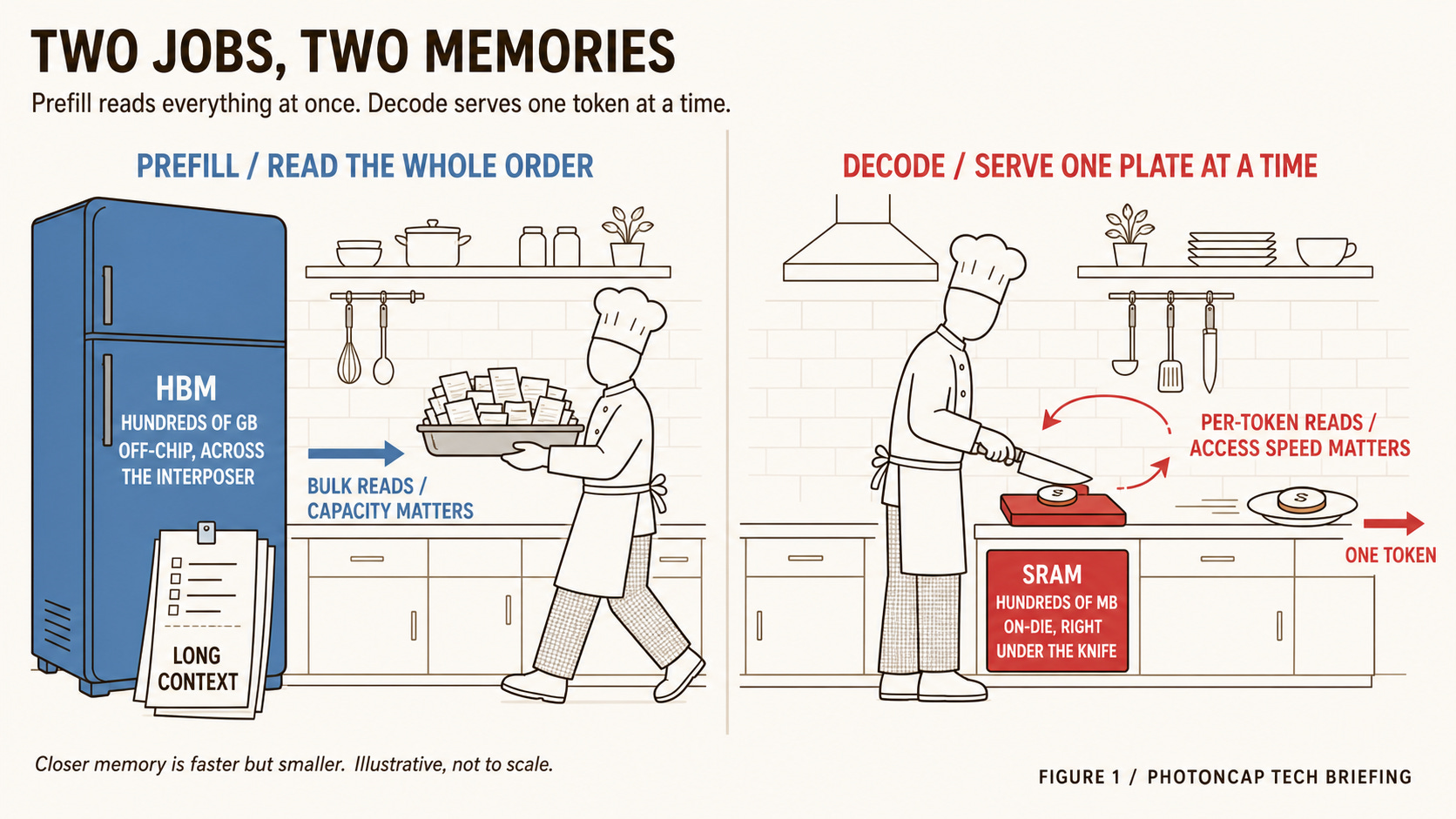
Figure 1: Prefill vs decode, the big fridge (HBM) and the fast cutting board (SRAM)
The natural next question: why not just make HBM faster? The reason it doesn’t work is physics. However close it gets, HBM sits outside the chip, across the interposer (the intermediate substrate that carries the chip and its memory). The distance signals travel through package wiring and the ceiling on pin count mean that raising bandwidth requires more stacks or faster pins, and both bill you in power, heat, and yield. SRAM sits on the same silicon as the compute units, so its cost structure is simply different. This capacity-for-speed trade is not the kind of constraint that process shrinks dissolve, and as we saw in Three Routes Around the Memory Wall, the industry has been engineering detours around it. Rack disaggregation is the most radical form of that detour. When the problem won’t yield inside the chip, you split the machine.
What matters here is that this division of labor is hardening into a hardware purchasing unit, not a software scheduling trick. Not time-slicing inside one rack, but standing up a separate rack filled with different silicon right next door. And once racks split, something has to connect them. That “something” is the rest of this piece.
The way system composition itself changes as workloads move from training to inference to agentic is exactly the diagram from the April piece.
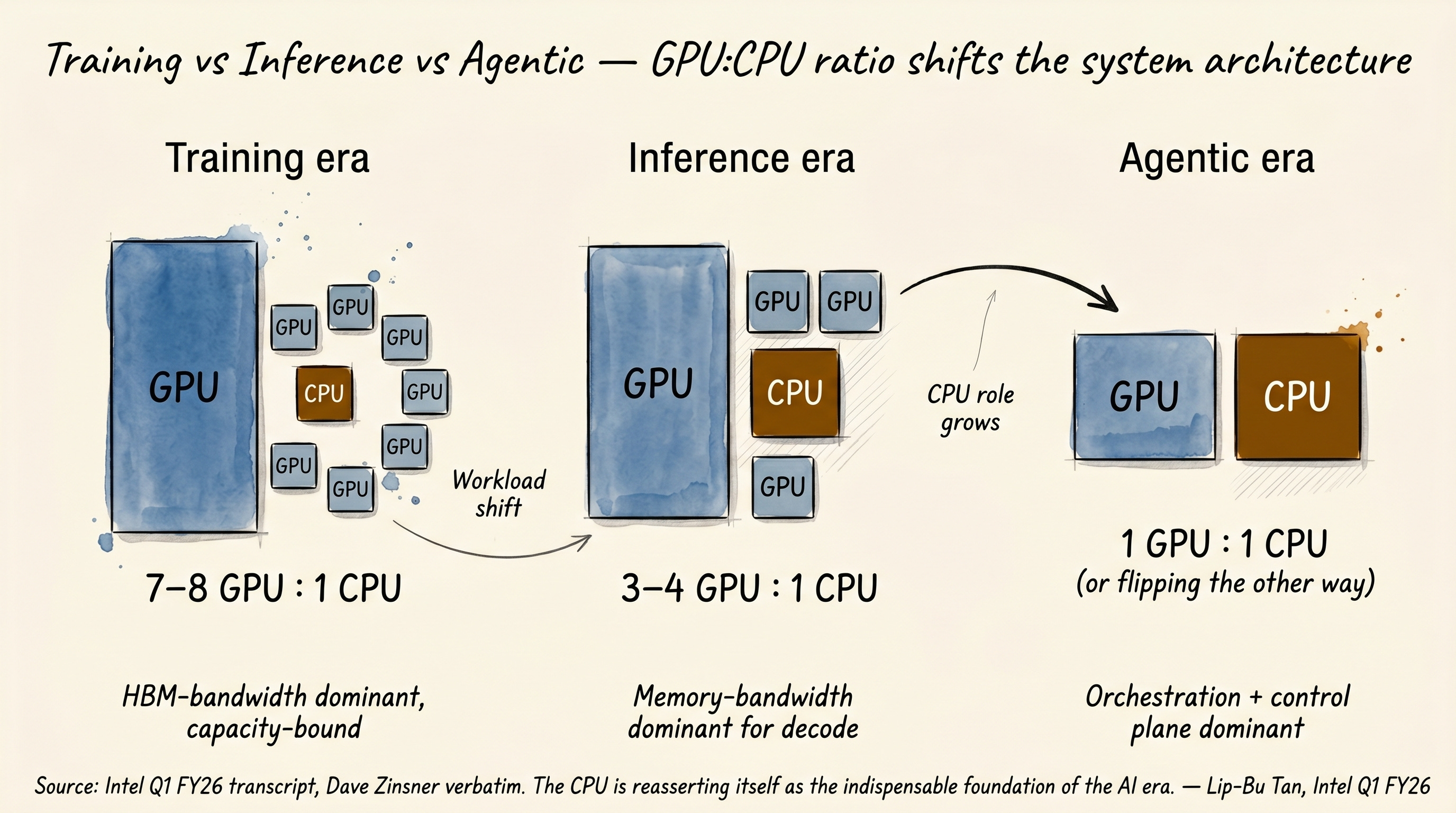
Training vs Inference vs Agentic, the GPU:CPU ratio shift reshapes the system. Reused asset from the April piece
The prequel to this structural shift, how workload bifurcation split the chips across multiple foundries, is in The GPU era ran on TSMC. The inference era runs on multiple foundries. That piece was about who manufactures the chips. This one is about what connects the racks.
3. They Wrote Down Everything Except the Wire
Everything up to here is confirmed by NVIDIA’s and AMD’s own public documents. That inference racks are splitting, which chips go into each rack and how many, how much bandwidth one rack pushes: all of it sits in the manufacturers’ own materials.
Except the one line an investor needs most.
NVIDIA’s LPX technical blog states that the GPU rack and the LPU rack exchange data every time a token gets made[1]. The frequency and the mechanics are described in detail. What is not written anywhere in the document is the physical layer between the two racks, whether that data rides copper or glass. Same on AMD’s side: the spec of the connection between Helios and the Cerebras machine appears nowhere in the announcement[2]. This blank is also a spot the previous piece left open on purpose. Three Routes Around the Memory Wall flagged the disclosure of the interconnect between the two engines as the first data point that would update its middle-shell call, and that disclosure hasn’t come. So instead of waiting, this piece lines up what has been disclosed, segment by segment, and narrows the candidates for the blank.
The blank may look small, but the direction it gets filled rewrites the entire beneficiary list. If it’s copper, this is a connector and retimer market. If it’s light, the road forks again. Plug-in transceiver modules mean revenue for component makers like $COHR $LITE. CPO (co-packaged optics), where the optical parts get packaged onto the switch chip itself, shrinks the socket for plug-in modules on the switch side and redistributes the revenue across switch vendors, optical engines, and the external laser supply chain. If the four form factors are new to you, the whole ladder is laid out in DSP, LPO, NPO, CPO: The Four Optical Architectures and the Light Source Beneath Them All.
The first-order variables that pick copper versus light are distance, signal speed, and power. The meter or so inside a single rack is where copper is cheapest and most stable, and over short runs a direct copper link, with no conversion of electricity into light, can even win on latency. Past the tens of meters that cross a hall, copper’s signal loss stops being manageable and light is the only practical option. The problem is the awkward few meters in between, the next rack over, the next row over. In that zone, the traffic pattern does not pick the medium directly; it tightens the constraints. Occasional bulk traffic leaves you freedom in placement. A loop that never stops shrinks the allowable latency and the number of switch hops, which changes where you can even put the two racks.
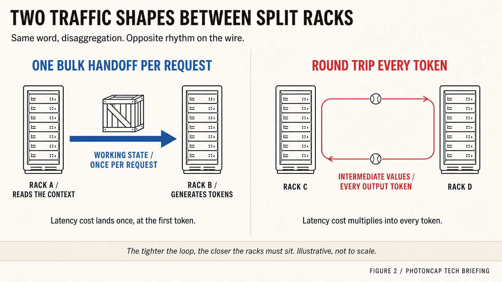
Figure 2: Two traffic shapes between split racks. One bulk handoff per request vs a round trip every token, camps unlabeled
Rearrange the two companies’ public documents against those criteria, segment by segment, and you can close much of the blank: which segments are already locked to copper, which segments have which kind of light written down, and which segments are simply empty. At the end of that arrangement, one spot emerges where both camps converge. That spot is where the paid section begins.
Let me show you the paragraph itself first. This is the NVIDIA passage that says the two racks trade data on every single token. Read it to the end and it never says what the data rides on.
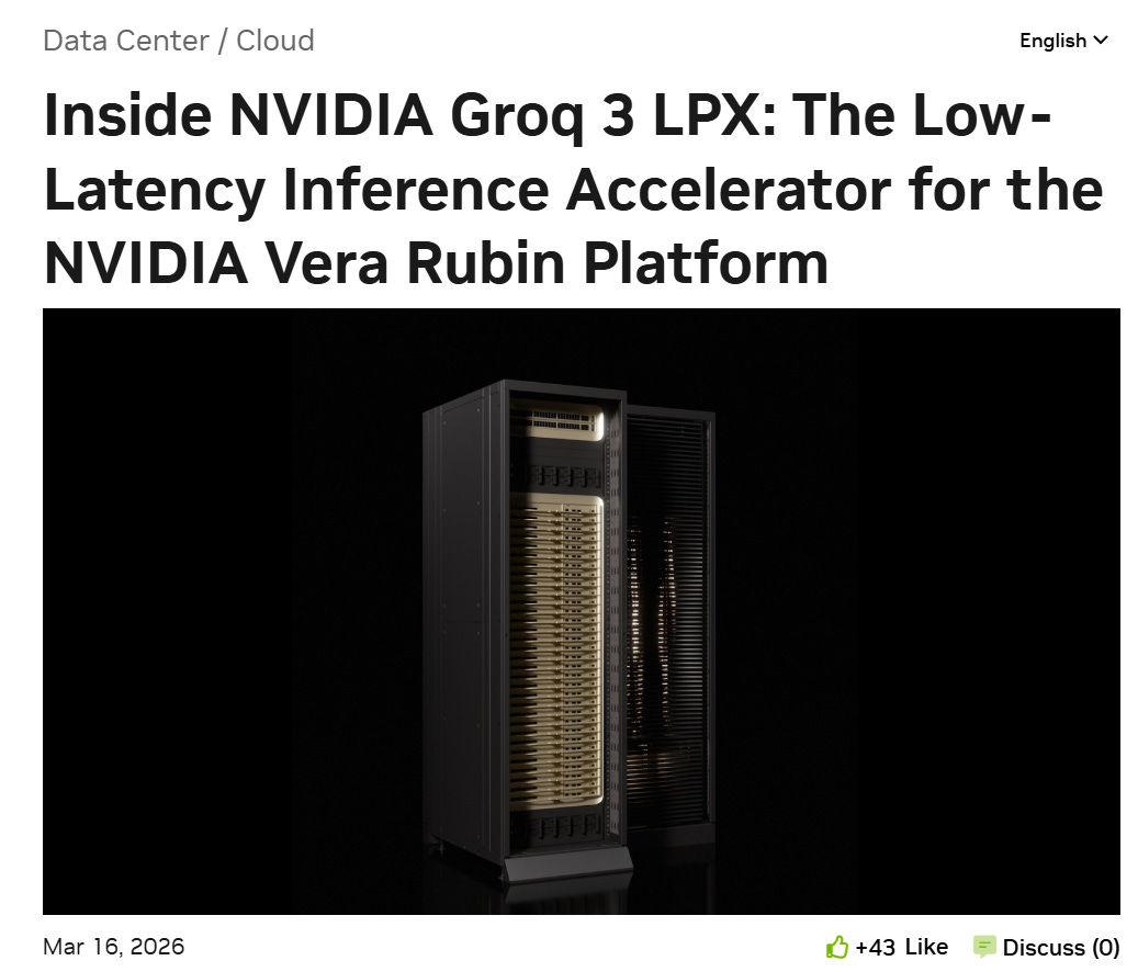
Screenshot: NVIDIA LPX technical blog excerpt. Source: NVIDIA Developer Blog, 2026-03-16
Key point: rack disaggregation is a fact settled by public documents. What is not settled is the physical link between the split racks, and the direction of that answer redraws the exposure map of the optical component names.
4. AMD’s 2 Pieces + NVIDIA’s 5
What NVIDIA unveiled at GTC 2026 was not two racks but a POD built from five kinds of specialized racks[6]. Forty racks, 1,152 Rubin GPUs, bound into one supercomputer, and the division of labor inside is what deserves the attention.
NVL72 is the compute engine. It binds 72 GPUs and 36 Vera CPUs over an NVLink copper spine (the bundle of links running vertically up the back of the rack like a backbone) and takes prefill plus the part of decode that decides which slice of context to consult, the calculation called attention[6]. Per NVIDIA, Vera Rubin has entered its full production ramp with partner systems being built and shipped, and broad availability is slated for the second half of 2026[6][7]. LPX handles low-latency generation, the 256-LPU configuration from above[5]. The Vera CPU rack runs up to 256 CPUs per rack, hosting 22,500 concurrent agent sandboxes[6]. BlueField-4 STX is the storage rack that offloads, stores, and serves context memory including the KV cache (the working memory a model piles up to remember the conversation so far)[6], and Spectrum-6 SPX is the networking rack that ties all of these together[6].
Extend the restaurant: kitchen (NVL72), speed line (LPX), front office (Vera CPU), pantry (STX), and hallway (SPX), five rooms carved out of what used to be one. The pantry is the one to stare at. The KV cache, the model’s record of “what I’ve read so far,” moves out of the HBM next to the GPU into its own rack and travels the network, which means memory itself becomes traffic that crosses rack boundaries.
AMD’s announcement is simpler. Helios stands as the high-throughput general engine, and only the latency-critical decode and token generation gets handed to Cerebras’s wafer-scale machine, a PD disaggregation structure that splits prefill and decode at the node level[2]. The joint configuration is expected to be available first through Cerebras Cloud in the second half of 2026[2]. The companies claim up to 5x higher tokens per second per watt for the combined setup, a vendor modeling figure comparing Helios plus WSE against a WSE-only configuration, not against Helios alone and not against an existing GPU rack[2]. No customer benchmark exists yet.
One thing to pin down before moving on. “Five versus two” is not a comparison drawn on the same boundary. NVIDIA’s five counts the entire POD by function, compute through storage through networking. AMD’s two counts only the inference compute path; an AMD deployment obviously has its own networking and storage infrastructure besides. What this piece is comparing is not rack counts but where the inference path gets cut. Read that location through a traffic lens and the camp with more pieces, NVIDIA, is actually the one carrying the tighter requirement. The next section explains why.
5. Once per Request, Once per Token
The two camps cut in different places.
AMD and Cerebras’s PD split cuts between prefill and decode. In a typical PD disaggregation, once the prefill side finishes reading the context, its output, the KV cache, gets handed to the decode side, and the cadence of that handoff is closer to per request than per token[8]. The left panel of the chapter 3 figure: a truck hauling goods from the warehouse to the storefront. That transfer is not free of latency, though. By the arithmetic in DistServe, the paper that formalized PD separation, the KV cache of a single 512-token request runs about 1.1GB, and serving 10 requests per second needs roughly 90Gbps, which is why bandwidth-aware placement is a design precondition; in its experiments, over 95% of requests completed the transfer within 30ms, and that cost lands on the wait for the first token (TTFT)[8]. AMD and Cerebras have disclosed nothing about their own implementation’s data movement or cadence, so this paragraph is PD disaggregation in general[2].
NVIDIA’s side is on the record. What the license[3] bought is Groq’s LPU technology, and AFD (Attention-FFN Disaggregation) is the name NVIDIA gave to the serving structure that pairs that LPU with a GPU[1]. This scheme cuts again, inside decode. The loop runs like this: the GPU computes attention over the accumulated KV cache and hands the intermediate values to the LPU; the LPU executes the FFN (the calculation that turns what was consulted into actual output) and the MoE experts (specialist sub-blocks that divide the labor inside the model) and returns the result to the GPU. In NVIDIA’s own words, this exchange repeats for every single output token[1]. The right panel of the chapter 3 figure: a ping-pong rally between two racks, one volley per word. Dynamo runs the orchestration, and NVIDIA’s own diagram draws the loop spanning both racks[1].
Same word, disaggregation, but the bill arrives at different counters. PD’s transfer cost lands mostly at the request boundary, the wait before the first token appears. AFD’s exchange cost sits inside the token generation loop, so its latency multiplies straight into the feel of every token. Aim at 1,000 tokens per second[1] and the entire cycle for one token, compute and communication combined, is about 1ms. The latency budget for a round-trip exchange has to be far smaller than that.
This is where distance enters. The deeper the exchange sits inside the loop, the closer the two racks must physically stand; the more the cost is paid at the request boundary, the more freedom you have in placement. Where you cut determines the traffic’s character, and the traffic’s character determines the latency budget and allowable distance. Medium selection is decided first by distance, signal speed, and power, and the repetition inside the loop then tightens the allowable latency and hop count further.
