
TL;DR
Of the roughly $2 billion in letters of intent (LOIs) the US Commerce Department signed with nine quantum companies in May, 68% went to quantum manufacturing technology development at two foundries, IBM and GlobalFoundries. But industry analysis puts the annual wafer volume for quantum chips at tens to hundreds of wafers, so this support can’t be explained by wafer revenue.
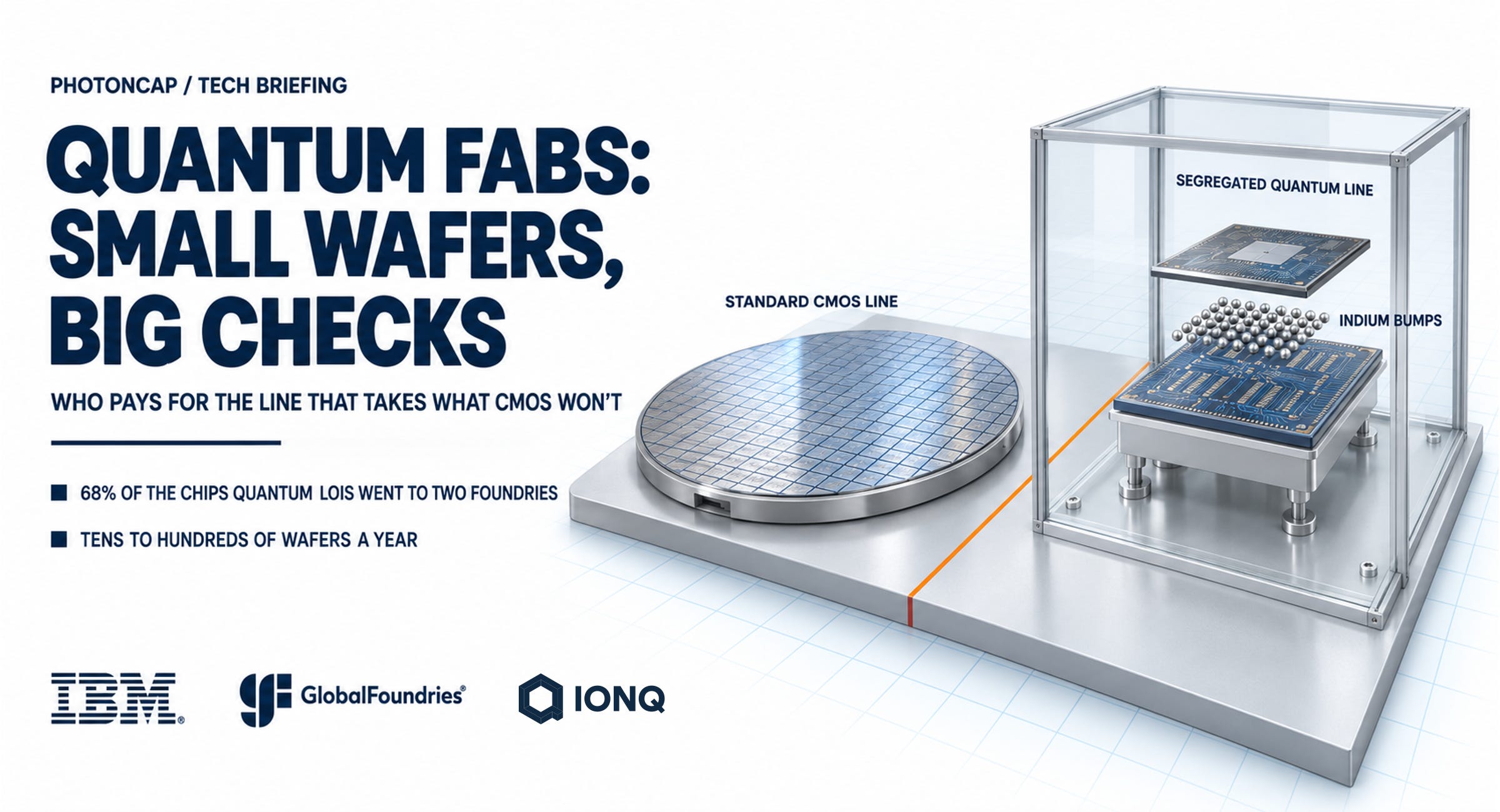
I think what a quantum foundry actually sells is a segregated line, kept apart from the ordinary chip fab line. The three layers are the materials that fab won’t accept, the processes it doesn’t use, and the bump stage where chips are bonded and stacked, and this is mostly a superconducting story. Underneath sits an ultra-precision processing problem that has nothing to do with the approach, so photonic and semiconductor spin chips also need lithography to define their patterns as intended.
Silicon spin and photonic chips have already gone the route of adding modules onto commercial 300mm lines, trapped ion is heading that way too, and superconducting is where the need for a segregated line is most pronounced right now. But the superconducting merchant lines open today (commercial lines that take in and fabricate other people’s chips) are held by companies that sell their own qubits or processors, like IBM, IonQ and QuantWare.
Cross-checking the documents turned up a case where a superconducting company that hands its core wafer processing to an outside foundry wrote the very fab a competitor had bought straight into a government agreement after the acquisition. My read is that the value of this business is decided less by wafer count than by who holds the segregated line.
Contents
68% and the Wafer Count
The Places Called “Quantum Foundries”
The Segregated Line
Where Each Qubit Type Gets Made
Why the Government Paid First
Three Deals of 2026: Anderon (IBM), IonQ and SkyWater, GlobalFoundries
Korea’s Quantum Fabs
Scale Math and Where the Value Accrues (Paywall)
What the Quantum Business Is Worth, Seen From the Fab
Looking Back at the September Investment Map, and the Dates to Check
1. 68% and the Wafer Count
On May 21 this year, the US Commerce Department signed letters of intent worth $2.013 billion with nine quantum companies. Of that, IBM gets $1 billion and GlobalFoundries (GF from here on) gets $375 million, and both are money for developing manufacturing technology at foundries that fabricate quantum wafers, rather than for developing qubits (the computing unit of a quantum computer). Together the two come to 68% of the total.
The number of wafers going into those fabs is much smaller than you’d think. Quantum Computing Report (QCR from here on), an outlet that analyzes the quantum industry, figured that for quantum chips annual wafer volume could run tens to hundreds of wafers. I first saw this framing, judging quantum fab economics by wafer volume, in that analysis. For comparison, last year GF shipped a whopping 2.34 million-plus wafers, in 300mm equivalents. A wafer is the round silicon disc that semiconductor chips are fabricated on, and 300mm is its diameter.
The stock prices raise the same question. As of the October 23 close, GF is up about 30% over one year, while IonQ, which went as far as buying a fab outright, has fallen by nearly half. That said, it’s fair to say what pulled GF’s stock up was expectations around silicon photonics (the technology of patterning circuits that carry light on a silicon chip) and US-based manufacturing more than quantum, and quantum’s effect on GF’s stock price is still barely visible.
So with revenue this small, why did the government put money into fabs, and why did IonQ go as far as buying one? On the silicon photonics side, I laid out who can actually fabricate optical chips in The Silicon Photonics Foundry Layer: Who Can Actually Make a PIC, and this time I put the same question to quantum chips. After writing the silicon photonics foundry piece and the September quantum investment map, what was left blank between them was the fabs that make quantum chips.
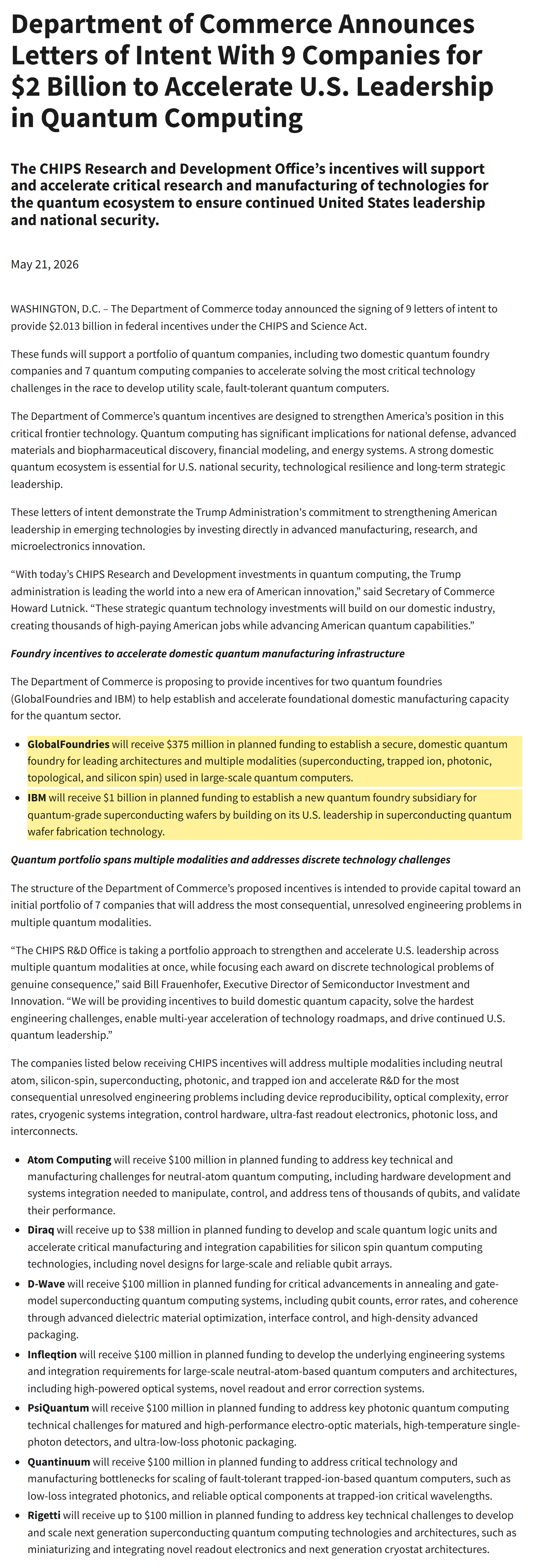
The nine-company list in NIST’s May 21, 2026 release, with the IBM ($1 billion) and GlobalFoundries ($375 million) lines highlighted.
2. The Places Called “Quantum Foundries”
A foundry is a fab that fabricates chips other people designed, on their behalf. A quantum foundry means the target is quantum chips, and that covers not just qubit chips but trap chips that levitate and hold ions, photonic chips that make qubits out of light, and even chips that control and read out qubits at cryogenic temperatures.
The problem is that the same name gets attached to facilities that are pretty different in character. First there’s the commercial contract line that takes money to fabricate other people’s wafers, which the industry calls a merchant line. IBM’s subsidiary Anderon, GF’s Quantum Technology Solutions and SkyWater’s Quantum Solutions fall into this group, while the Netherlands’ QuantWare, which says it already offers a contract service fabricating superconducting chips from customer designs, is scaling up with a new fab, and Denmark’s Quantum Foundry Copenhagen is under construction. There’s also the national lab shared service. MIT Lincoln Laboratory’s SQUILL gathers just over a hundred user designs per wafer, in several sets, and fabricates them. This approach of gathering multiple designs onto one wafer is called MPW (multi-project wafer).
There are also open research fabs where researchers run the tools themselves, and Korea’s KAIST National Quantum Fab falls into this group. Some places are foundries in name only, and UC Santa Barbara’s NSF Quantum Foundry is a research center that develops materials and devices for quantum information technology. Separately, there are in-house fabs, like those of Google, Rigetti and IQM, where companies make their own chips in their own fabs.
When this piece says quantum foundry, it means the merchant line.
3. The Segregated Line
A segregated line is a zone or line kept apart from the ordinary chip fab line, where the materials and processes that fab won’t accept are handled separately. An ordinary chip fab, which the industry calls a CMOS fab (the standard process line that makes most of today’s logic and memory chips), is strict about which materials come in. The prime example is gold. When gold atoms get into silicon, they create defect levels near the middle of the bandgap (trap sites that catch electrons and wipe them out), adding more places where electrons disappear. That’s why imec said it switched to a gold-free process when bringing gallium nitride power devices into a CMOS line.
Superconducting qubits are made from metals like aluminum, niobium and indium. Germany’s Fraunhofer EMFT splits its 200mm pilot line into a CMOS zone and a separate zone for non-CMOS materials like niobium and indium, and its paper says the wafers leave the CMOS line at the indium step. So the qubits themselves are made on the CMOS line, and the separation happens at the step after that.
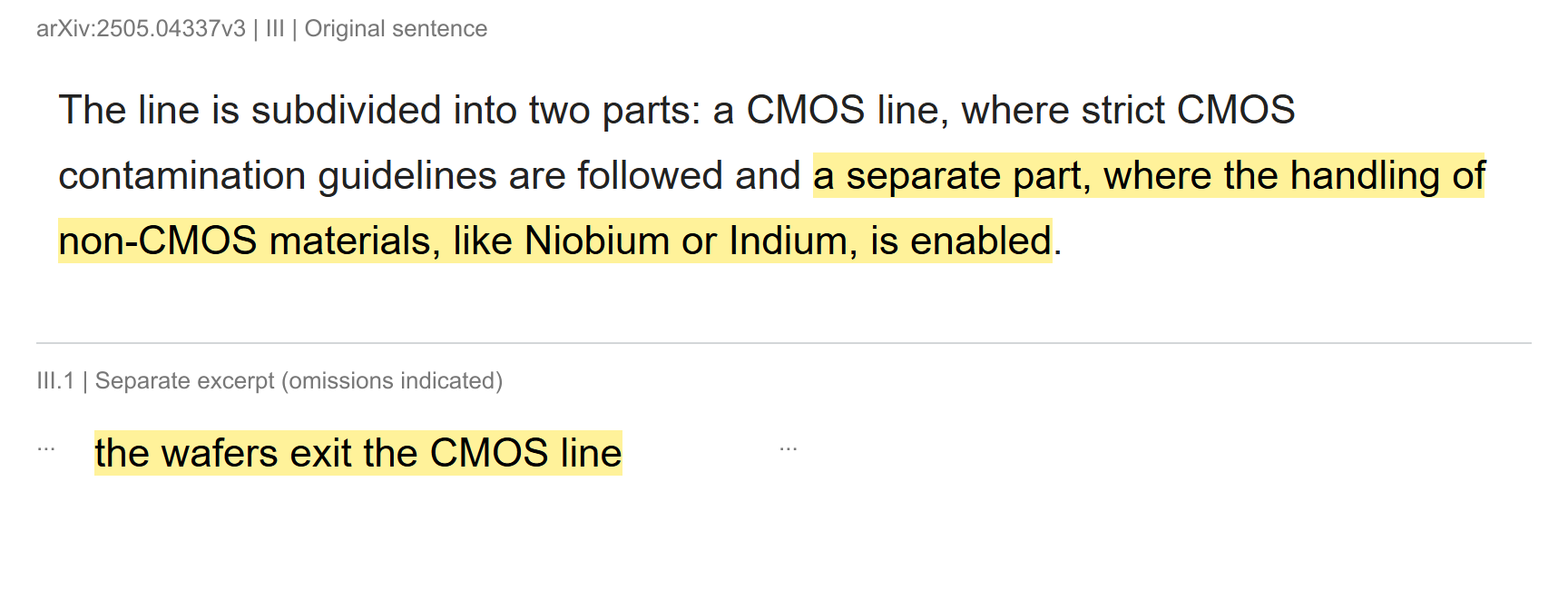
Two sentences from Fraunhofer EMFT’s arXiv 2505.04337, “a separate part, where the handling of non-CMOS materials, like Niobium or Indium, is enabled” and “the wafers exit the CMOS line”, highlighted. Source: Fraunhofer EMFT, arXiv 2505.04337, 2025
Process methods are a sticking point too. The standard lab processes are angle evaporation, which deposits at a tilt, and lift-off, which puts metal on top of a photoresist layer and then peels it off along with the resist, and imec wrote that these methods leave resist residue and lose reproducibility on wafers larger than small lab wafers, so they’re largely incompatible with volume manufacturing. Korean press coverage dealt with the same point. Money Today wrote that because lift-off isn’t a CMOS-compatible process, it’s hard for Samsung Electronics or SK hynix to produce superconducting quantum processors right away.
The stage where chips are bonded and stacked is a sticking point too. Flipping the qubit chip and the wiring chip to face each other and joining them with small metal protrusions (bumps) is called flip-chip, and Google’s Sycamore also joined its two chips with indium bumps. IBM putting superconducting wiring, through-silicon vias (TSVs) and bumps side by side on Anderon’s process menu is about the same stage. As qubit counts grow, you can’t lay all the wiring on one plane, so stacking becomes unavoidable, and then this stage keeps getting bigger.
But these three layers shift a bit from fab to fab and from payer to payer. For the niobium family, the call differs by fab. GF’s 300mm high-volume line already accepts the niobium nitride detector layer on PsiQuantum’s chips. In return, the two companies said in 2021 that they had installed proprietary production tools at two GF 300mm fabs (the New York fab for photonic chips, the Dresden fab for control chips). You can see it as a case of bringing separate customer tools into the fab to widen the range of materials it accepts. The opposite case is imec. imec used only aluminum and switched from lift-off to subtractive etch (a process that cuts away the parts you don’t need), and got 393 out of 400 qubits working on a 300mm CMOS pilot line. Rather than adding materials, imec in effect moved the process toward the fab’s rules.
So what’s the highest wall in getting past the three layers? It’s tempting to name a specific component like the Josephson junction (JJ), but my answer is short. It’s not something specific like the JJ, it’s ultra-precision processing. A JJ is a component with an insulating film a few atomic layers thick sandwiched between two layers of superconducting metal, and it sets the frequency of a superconducting qubit. Going by imec’s data, this junction’s resistance spreads by about 4% within a single chip and the frequency spreads by about half that, which for a 5GHz qubit is around 100MHz (an approximate calculation for those junction conditions). In an architecture where neighboring qubits can’t overlap in frequency, this spread directly determines yield, so IBM tunes the junctions by heating them with a laser on chips that have left the fab, and Rigetti trims the resistance spread with electrical pulses down to around 0.5%. At the junction you have to control a barrier a few atomic layers thick and its interfaces, and at the bumps and stacking you have to control contamination, alignment and contact uniformity. And ultra-precision processing applies just the same to the other approaches. Photonic chips and semiconductor spin chips alike only get the right loss and uniformity when lithography (the process of patterning circuits with light) defines the patterns as intended. Whether a segregated line is needed differs by approach, but I think this precision sits at the bottom of what a fab sells, whatever the approach.
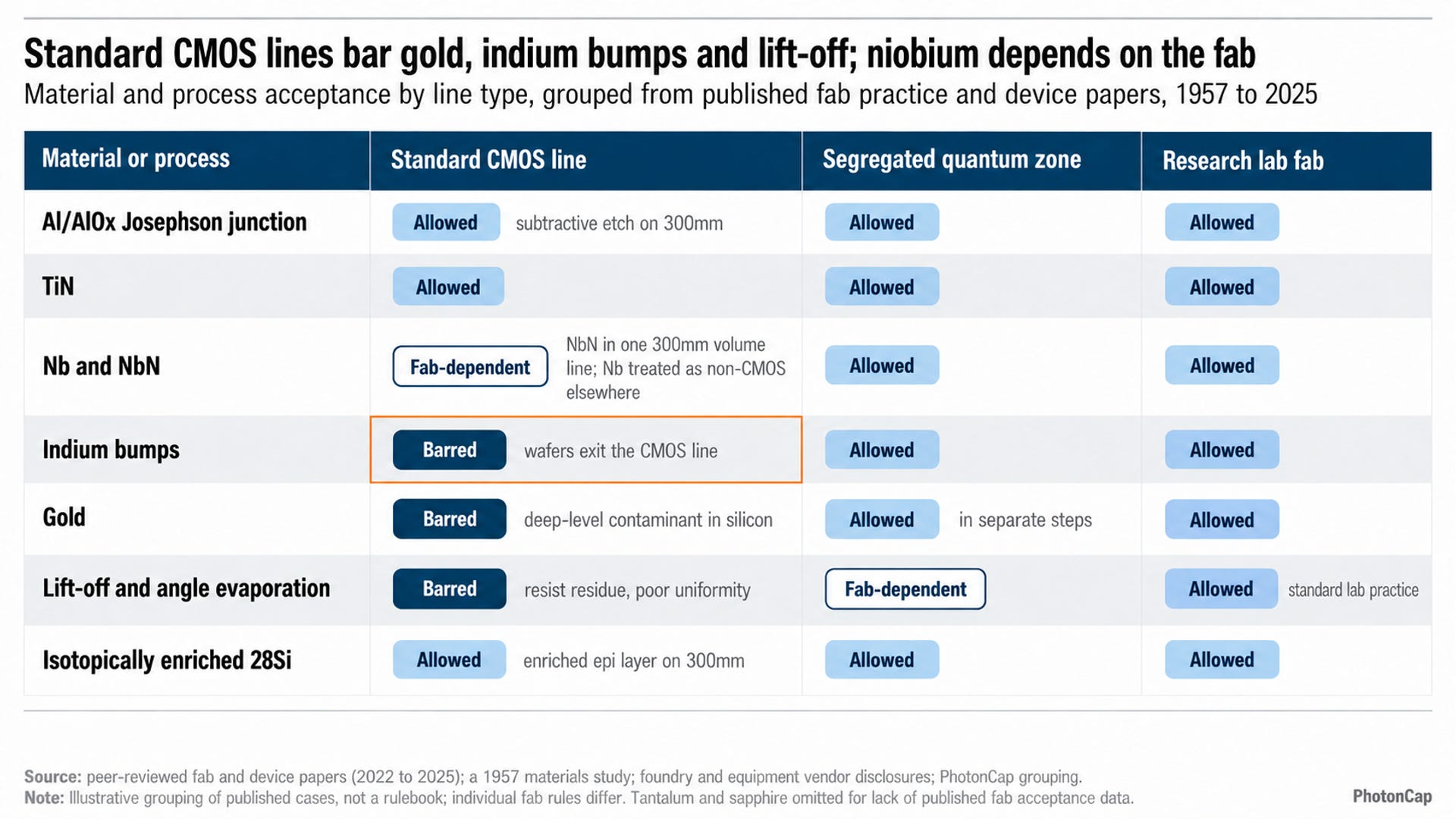
Material and process acceptance by line type: standard CMOS line, segregated quantum zone, research lab fab
The figure above groups the cases confirmed in primary sources by line type, and the thing to notice is that the “fab-dependent” cells take up more room than you’d expect. I left out Ta (tantalum) and sapphire substrates because there’s no primary source stating which fabs allow them.
4. Where Each Qubit Type Gets Made
Each approach asks different things of the fab, and so each one goes to a different fab.
Silicon spin qubits use the spin of a single electron trapped inside a semiconductor, so their process is the closest to that of ordinary chips. Intel made Tunnel Falls on its 300mm D1 line with a flow similar to a standard CMOS logic process and reported a 95% wafer yield. UK-based Quantum Motion fabricated a chip that put more than 1,000 quantum dots on 22FDX, GF’s low-power process (a quantum dot is a tiny cell that traps a single electron). What’s special here is more the materials than the process. They use silicon-28 with the isotopes that disturb the spin filtered out, and the chips have to be tested at cryogenic temperatures at the wafer level.
The photonic approach adds modules on top of a silicon photonics line. PsiQuantum makes its chips in GF’s high-volume fab and added a layer of superconducting detectors (SNSPDs) that catch single photons. Xanadu was already mixing several platforms at the time of Aurora. Going by the Aurora paper, Xanadu split the fabrication: the source chips in Ligentec’s silicon nitride (SiN) on an X-FAB line, the chips that pick and combine the source outputs in HyperLight’s thin-film lithium niobate (TFLN), and the computing chips on the AIM Photonics platform. This February it expanded its collaboration with Tower, and in October it announced a multi-year partnership with GF’s 300mm Malta line.
Trapped ion is the approach that levitates and holds ions in a vacuum with electric fields, and the trap chip is the chip with those electrodes patterned on it. As the field moves toward controlling qubits with on-chip electronics instead of lasers, the trap has turned into a question of electrode and wiring wafers. Infineon and Innsbruck researchers wrote in a paper that a single 200mm fused silica (quartz glass) wafer made at the Villach fab holds close to 500 trap chips, and Quantinuum named GF as one of several fabs that will make its next-generation ion traps on 300mm. That said, electrodes that withstand RF voltages of hundreds of volts and waveguides (paths for light on the chip) that carry light from ultraviolet to visible are still outside standard process design kits (PDKs).
Superconducting is the approach that most needs the segregated line from section 3. Google made Willow at its own fab in Santa Barbara, and Rigetti makes its chips on 150mm wafers at Fab-1 in Fremont, and it wrote in its 10-K that it expects this fab to meet all its own chip demand for at least the next three years. Finland’s IQM announced that it is expanding its domestic production fab. The main examples of superconducting merchant lines are Anderon and SkyWater in the US and QuantWare in Europe (GF has disclosed only as far as superconducting wiring, and Tower has no public material on the superconducting side), and OQC and Germany’s Fraunhofer EMFT announced that EMFT’s research pilot line will serve as UK-based OQC’s standard manufacturing site for quantum processors.
I made the point in Superconducting or Trapped Ion, They All Buy the Same Light: The Hidden Layer That Wires Quantum Computers Rack to Rack that whatever the approach, the part that links racks with light ends up buying the same components, but on the side of the fabs that make the chips, each approach goes a fairly different way. My outlook is that even for superconducting, the layers that form the qubits will move to commercial 300mm, as at imec, while the indium bumps, 3D stacking and packaging stages stay on the segregated line.
5. Why the Government Paid First
Each company gives a different answer for why these fabs are needed. Mihir Bhaskar, a former IonQ R&D executive who now runs SkyWater’s quantum business, wrote on the company blog that even IonQ’s CMOS-compatible trapped-ion hardware took more than six months to get a single round of wafers in 2025, and that the existing foundries’ terms were “no volume? No deal.” Rigetti’s CEO reportedly told IEEE Spectrum that what draws Rigetti to Anderon is process capability more than production capacity. Both are fair points, but I think the biggest reason these fabs are appearing right now is government money and supply chain security.
The evidence is the order the money came in. 68% of the letter-of-intent money went to two foundries, and the Commerce Department takes equity along with this money. Under its September agreement, GF agreed to issue 9.9 million new shares to the Commerce Department at $37.85 per share, which, divided by shares outstanding, comes to about 1.8% (calculated). D-Wave also signed its final agreement on the condition of a minority, non-controlling equity stake, and IBM also disclosed in its latest quarterly report (10-Q) that Anderon issued a minority stake to the Commerce Department. It didn’t disclose the percentage, and IBM keeps the controlling stake.
The regulators’ documents point the same way. In his July 31 statement on IonQ’s acquisition of SkyWater, the FTC Chairman called SkyWater a US-based quantum foundry and wrote that being an American company is an attraction for quantum computer developers. The same statement assumed that if competitors had to move foundries in a hurry, development could be delayed by several months, and it pointed to two new foundries funded by the Commerce Department as long-term alternatives. The names of those two, GF and IBM, appear in Commissioner Meador’s statement.
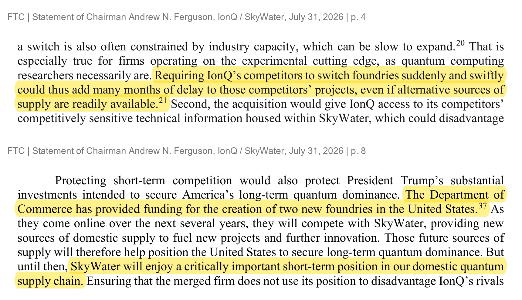
Page 4 of FTC Chairman Ferguson’s statement (”could thus add many months of delay”) and page 8 (”two new foundries”), highlighted. Source: FTC, Statement of Chairman Andrew N. Ferguson, July 31, 2026
In the end, the government didn’t wait for any particular qubit approach to win, and in effect started by buying fabs inside the US that can take any approach.
6. Three Deals of 2026: Anderon (IBM), IonQ and SkyWater, GlobalFoundries
Anderon (IBM)
Anderon is the quantum wafer foundry subsidiary that IBM announced plans to set up in May. In September the Commerce Department announced it had signed a final R&D award of up to $1 billion, and according to IBM’s latest quarterly report, about two-thirds of that became available with the agreement and the rest is released only when contractual milestones are met. The Commerce Department’s right to terminate for convenience and some clawback provisions are also attached. Separately, IBM said in May that it would put in $1 billion in cash plus IP, assets and people, and the same report says it has already put in that cash.
The fab itself is an existing line. It’s based on the 300mm line at Albany NanoTech in New York that IBM’s quantum team has been using for several years, and the complex is owned and operated by NY CREATES. Going by an IBM blog post, while the Yorktown research fab ran two shifts on weekdays, Albany runs wafers around the clock, every day. In September IBM said the first quantum wafers are running through the fab. In the launch announcement, IBM said this process is backed by a dedicated process design kit and by existing production capabilities such as inline wafer test, which measures wafers inside the line partway through the process. The first version of that design kit came out in October. Anderon said on its company blog that its first superconducting quantum PDK supports qubits, I/O components for signal wiring, amplifiers and filters, and can be tried early under a license agreement, but the public post gives no design rule numbers or materials. Headcount hasn’t been disclosed, but from what I’ve heard in the industry, it’s running for now at fewer than 100 people, carved out from some of IBM’s existing foundry engineers. It’s a number that hasn’t appeared in any official material yet.
There’s no named external customer yet. According to IEEE Spectrum’s reporting, Anderon CEO Mukesh Khare said it can deliver to external customers by year-end, and the same article has a passage saying Rigetti is in talks with Anderon. Anderon said Rigetti CEO Subodh Kulkarni shared the stage with Khare at Quantum World Congress in late September, but the two companies haven’t announced a contract yet. The modifier also changed several times over four months. In May it was America’s first pure-play quantum foundry, in IBM’s July investor letter it was the world’s first pure-play quantum wafer foundry, and in September it was the world’s most advanced pure-play quantum foundry, while the body of the quarterly report from that same July just said pure-play quantum wafer foundry, with no modifier. When you line these things up and compare them, there’s always one like this that turns up.
IonQ and SkyWater
IonQ announced its acquisition of SkyWater in January and closed the deal at the end of July. SkyWater shareholders received both cash and IonQ stock, and as of the announcement the equity value was around $1.8 billion. SkyWater was originally a specialty foundry with a 200mm fab in Minnesota, and it also holds Trusted Foundry accreditation certified by the US Department of Defense’s DMEA. It now also has facilities in Florida and Texas. 2025 revenue was in the $440 million range, and in the same release the company said it had eight development projects with quantum computing companies.
What does it tell us that SkyWater, a quantum foundry, got acquired by IonQ? That’s how much it matters. In a word, my take is that if you hold the fab, you buy time. IonQ said that co-developing with SkyWater cut its design cycle from nine months to two, and that over six months it ran 12 times as many wafer lots (batches of wafers that run together at once) as at its previous foundry. That’s the company’s claim, and the previous foundry isn’t named.
On the surface, SkyWater keeps running its quantum business separately from IonQ. In fact, in September SkyWater launched SkyWater Quantum Solutions for external customers and rolled out SC250, which puts a Josephson junction layer on top of multilayer niobium wiring, and SP90, a silicon nitride photonics platform. SkyWater said the first SP90 wafers have already shipped (the full platform is slated for 2027), and Qolab, whose CTO is John Martinis, who used to lead Google’s quantum hardware, signed a multi-year agreement as SC250’s lead customer, for its QSiP, which bundles cryogenic wiring, filters and amplifiers into one package. Structurally, though, SkyWater is a wholly owned subsidiary of IonQ, and that subsidiary is a merchant line that also takes other people’s wafers.
For reference, SkyWater said in 2022 that it would build a large fab on the Purdue campus (it wasn’t going to be quantum-only) and then dropped the plan in 2024, IBJ reported, and that same SkyWater is now an IonQ subsidiary.
GlobalFoundries and Tower
GlobalFoundries is well known, of course. Honestly, it’s been that way for a long time. PsiQuantum has been developing photonic chips with GF since 2019, and on the spin side, Quantum Motion, Equal1 and Diraq have also teamed up with GF. But it was with the launch of Quantum Technology Solutions this May that GF made this official as a “new quantum business.” On September 8, the Commerce Department’s CHIPS award of up to $375 million was finalized, and the same day Quantinuum listed GF as one of several fabs that will make its next-generation ion traps. On October 6, Xanadu announced a multi-year partnership that puts its detectors and silicon nitride on GF’s Malta line.
Superconducting has to be looked at separately. GF said it is “developing” manufacturing platforms for quantum processors across several approaches, including superconducting, and the superconducting items currently listed on its technology page are cryogenic readout and control chips and superconducting interconnect. No contract manufacturing track record with external superconducting qubit customers has been disclosed yet.
Tower has a silicon photonics line just as GF does, but its quantum exposure is much thinner than GF’s. As far as I’ve checked, the only case of a quantum company appearing as a partner in Tower’s disclosures since 2021 is the one Xanadu deal, and the body of its 2025 annual report doesn’t contain the word quantum. I see Tower as an AI silicon photonics foundry with a quantum option attached.
7. Korea’s Quantum Fabs
In academia, a KAIST quantum fab is taking shape. The KAIST National Quantum Fab will take more than KRW 45 billion through 2031, and the targets are completion in 2027 and full operation in 2028. Its operating model is fully open, with researchers running the processes themselves, and the supported platforms in the official wording are photons, point defects and neutral atoms. Director Yong-Hoon Cho reportedly said, in effect, that they prepared the photonics side first because a superconducting quantum fab already exists in Korea.
The interview doesn’t name that fab, but the place that checks out as having made superconducting qubit chips in Korea is Sungkyunkwan University’s QFab in Suwon. QFab describes itself as a quantum foundry that makes superconducting qubit devices for researchers, and it runs chips every quarter on 3-6 inch wafers. It was also reported that, for the 20-qubit superconducting system KRISS (Korea Research Institute of Standards and Science) unveiled in 2024, qubit design and fabrication were handled by Sungkyunkwan University and UNIST. On the photonic side, KOSDAQ-listed Sawnics is taking part in a KRW 10 billion quantum photonic integrated circuit foundry project led by KAIST. UNIST also opened a KRW 30 billion quantum nano fab this spring.
In other words, Korea has split the roles, with superconducting at Sungkyunkwan University and photonics at KAIST, and the spot for a merchant line like Anderon or GF is still empty. In September the Ministry of Science and ICT designated Seoul, Jeonnam-Gwangju and Busan-Ulsan-Gyeongnam as quantum clusters, and Daejeon, home of the National Quantum Fab, was reportedly left out this time.
That’s it for Korea. But one thing caught my eye while cross-checking US filings. The agreement D-Wave signed with the Commerce Department on September 4 has a list of project sites, and SkyWater’s Minnesota fab is on that list. That date is a little over a month after IonQ closed its acquisition of SkyWater.
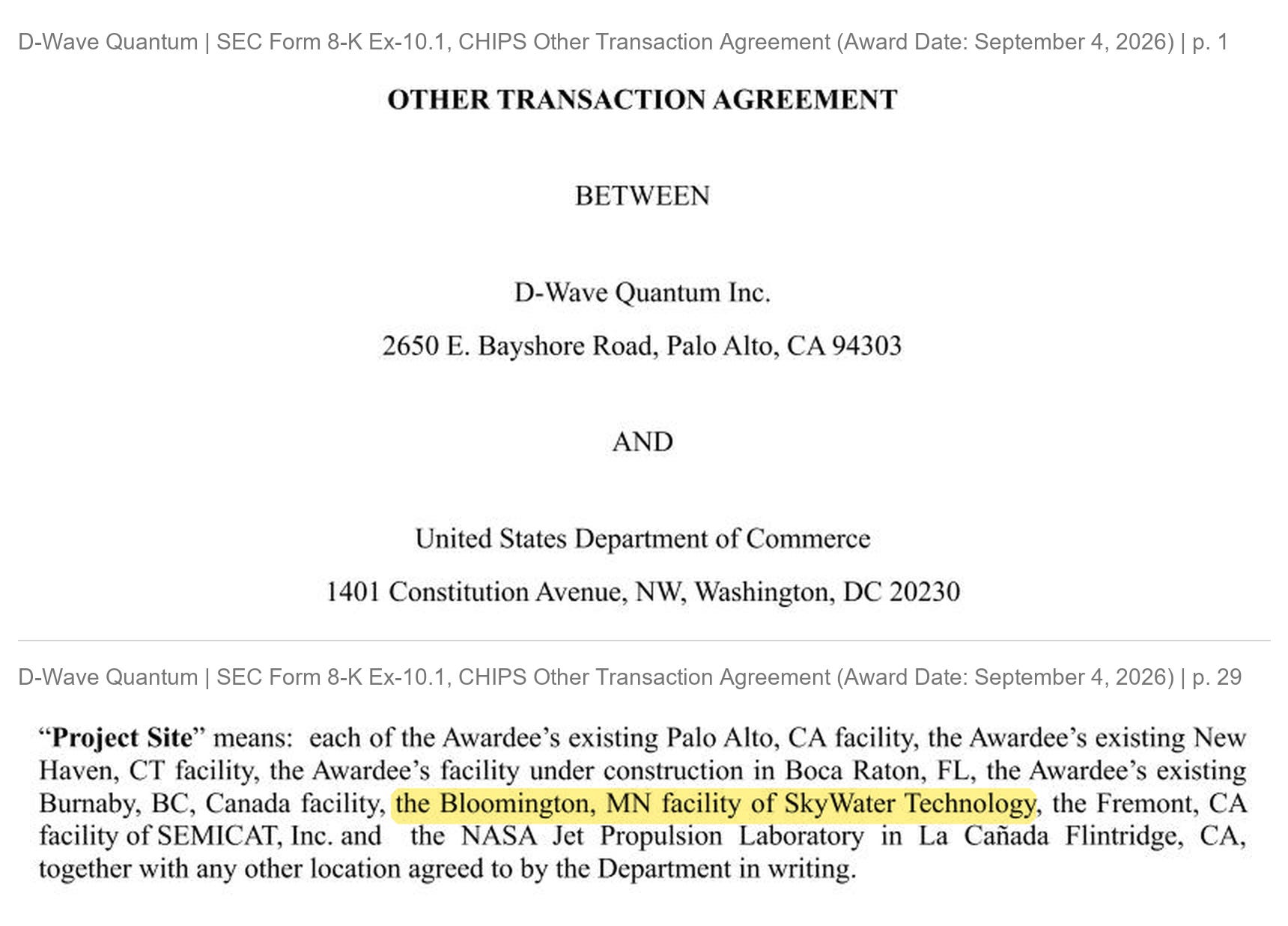
The “Project Site means” definition in D-Wave’s CHIPS Other Transaction Agreement (8-K Ex-10.1), with “the Bloomington, MN facility of SkyWater Technology” highlighted. Source: D-Wave Quantum, SEC 8-K, September 8, 2026
Why would they write a fab that a competitor bought straight into the agreement? The paid section starts from this one line and moves on to who that value accrues to and to listed-company exposure.
