
Abstract
On November 2, Marvell agreed to buy Lumentum, and three days later SemiAnalysis published a benchmark showing Google’s TPU can go head to head with NVIDIA’s GPU on inference token cost. I read the two separately at first and then ended up putting them side by side, and once I did, the question shifted a little. How cheap one chip is matters, but how many chips you can tie together as one body is becoming the thing that sets inference cost. And on whether you build that domain out of copper or out of light, NVIDIA and Google are standing in fairly different places right now. One thing caught on me while I was digging: an optical switch wasn’t the only thing Marvell bought. My view is that in large-model inference, where chip-to-chip communication becomes the bottleneck, whoever has run optically stitched domains first will stand in the better spot in the price fight over the next two years.
(as of 2026-11-19)
Contents
The Day Marvell Bought Lumentum
Why Wiring Became a Problem Only Now
72 on Copper, and 1,000 on Copper Mixed with Light
NVIDIA Said It Is Putting in CPO. What About Rack to Rack?
Marvell Did Not Buy Only a Switch
The Bigger the Domain, the Stronger OCS Gets
Dates to Watch
1. The Day Marvell Bought Lumentum
On November 2, Marvell announced it would acquire Lumentum in an all-stock deal at an enterprise value of $115 billion. Lumentum shareholders get 4.5 Marvell shares per share, and closing is set for the first half of 2028. The Lumentum assets the press release names as the rationale are high-performance lasers, optical transceivers, OCS (Optical Circuit Switch, a switch that reroutes the path of the light itself without converting it to electricity), and compound semiconductor manufacturing.
Most of the coverage put OCS up front, but my eye went to the lasers first. Lumentum is a company that owns its own InP (indium phosphide, the compound semiconductor that telecom lasers are made from) fabs. And in July this year it signed a six-year capacity reservation agreement with AXT, which makes InP substrates. According to AXT’s filing, AXT sets aside a minimum volume for Lumentum every year, and in return Lumentum pays a deposit of close to $90 million in two installments. It put down a deposit with a substrate company to hold six years’ worth of seats.
Here’s what went through my head when I saw this. Ah, Marvell is trying to go vertically integrated from the chip all the way to the light. And somebody is behind this.
NVIDIA and Google both get named as that somebody. NVIDIA invested $2 billion each in Marvell and Lumentum in March this year, and a Bloomberg report that Jensen Huang, CEO at the time, backed this merger was cited across several outlets. CEO Murphy also said in a CNBC interview on the day of the announcement that the reaction from NVIDIA was very good. Huang then stepped down as CEO on November 12, and CFO Colette Kress is serving as interim CEO. The board said it expects the product roadmap to continue without interruption. On the Google side there is a filing. In August Marvell disclosed a commercial agreement to develop custom chips for Google, covering inference accelerators and various controllers that attach to the TPU ecosystem, and Google received a warrant to buy about 59 million Marvell shares. Most of that warrant vests in pieces each time revenue from those custom products accumulates another $500 million.
In Marvell Buys Lumentum: What If NVIDIA Set Up the Play?, posted the day after the deal, Damnang laid out four scenarios on the assumption that NVIDIA was deeply involved in it. One of them is a picture where Google’s TPU gets a second full-stack supplier besides Broadcom. The author notes that all of it is speculation, and I don’t know who set up the board either. What can be confirmed stops here. NVIDIA put money into both Marvell and Lumentum, and Google has a contract with Marvell for chips around the TPU. Nothing has been confirmed about Google buying Lumentum components or backing this merger.
Why would two companies that compete with each other each have a line into the two companies that are about to merge? I think the answer is in the wiring between the chips, more than in the chips.
2. Why Wiring Became a Problem Only Now
Until a few years ago, wiring wasn’t something people talked about. You plugged eight accelerators into one server, connected them with copper traces on the board, and that was it. Servers were connected to each other over an ordinary network.
But as the number of chips that have to be tied into one body grew, things changed. To connect more chips to each other at the same speed, ports and switches and cables all grow together. Putting 72 chips in one rack and connecting every one to every other takes thousands of cables, and the first thing you run out of is the physical space to route them. Next comes loss. The higher the signal speed, the more copper attenuates the signal even over short distances, so at today’s speeds it’s hard to get out of a single rack. There are more wires, and each one reaches a shorter distance. At the OCP Global Summit this past October, a good share of the talks were hanging on this problem too.
There is a reason on the model side why this problem got more urgent in inference. Today’s large models don’t fit on one chip. Many use the MoE (Mixture of Experts) structure, which keeps several small neural networks that act as experts and picks among them as needed, and the longer an agent works, the bigger the KV cache, which is the equivalent of the conversation record, gets. So the model ends up split across dozens or hundreds of chips, and the split pieces have to exchange data with each other every time a token is produced.
This is where the unit called a domain comes in. A set of chips tied together with dedicated high-speed links and used as one body is what NVIDIA calls by the rack and Google calls a pod. When that communication ends inside the domain, it’s fast and cheap. The moment it leaves the domain and rides the ordinary network, latency gets added and more equipment goes in. So a bigger domain gives you more options for placing a large model and its KV cache. A bigger domain doesn’t make inference cheaper on its own, and the effect shows up in the cases where communication is the bottleneck.
Prices are already coming down fast. On its November 17 earnings call, NVIDIA said token prices have fallen nearly 60% since May. If prices drop at this pace, the side making the tokens has to cut cost by that much to hold on.
The TPU inference benchmark SemiAnalysis put out on November 5 was the starting point for this piece. It’s work that loads the same model on several chips and measures cost per token, and it’s welcome in itself that public measurements like this are piling up. SemiAnalysis compared with the actual serving configuration and software optimization included. What I want to look at next to it is the share of those results that comes from how the chips are physically stitched together, and the benchmark numbers alone can’t pull that share out. Software like TPU Sync, which Google unveiled on November 9 and which moves the KV cache between memory and the network, changes serving performance too. So this piece looks at structure in place of numbers.
3. 72 on Copper, and 1,000 on Copper Mixed with Light
NVIDIA’s current mainstay, NVL72, is just what the name says, a domain of 72 GPUs tied together with copper inside one rack. Copper is cheap, draws almost no power, and is fully proven. The reason NVIDIA worked so hard to cram 72 into one rack was to fit as many as possible within the distance copper can reach.
Google came by a different road. Look at TPU 8i, the inference TPU it announced in April this year: four chips are fully connected to each other on one board, and eight of those boards are tied with copper cables into one group. Up to here Google is on copper too. Then 36 groups are stitched together by optical links that pass through OCS to make one pod. According to Google’s technical write-up, this connects up to 1,152 chips, 1,024 of which are used for actual compute, and any chip reaches any other within seven hops. Google calls this structure Boardfly and said it cut network diameter by more than half. That is the company’s statement, and the number has not been verified externally.
TPU 8t, the training version, is bigger. One superpod is 9,600 chips, and when a link fails, OCS is said to rebuild the configuration without human hands.
On November 9 it announced two more systems. TPU 8i Max, which puts two TPU 8i chips in one package, and TPU 8tx, which handles confidential inference for enterprises and governments. AMD announced the same day that TPU 8tx uses AMD’s 5th Gen EPYC as its host CPU, and most headlines went with AMD getting its CPU into Google’s rack. AMD now competes with NVIDIA with its own racks while supplying the CPU for Google’s TPU racks. But my eye went to a different line in the same announcement. According to Google, TPU 8tx uses the same silicon as the training 8t, and for the way the chips are stitched it brought over Boardfly, which was built for inference. Google said that this brought latency down to as little as half that of 8t. The host CPU and the security features changed along with it, so it’s hard to read this as a number that measures only the wiring’s share. Still, I think it’s a case where Google showed, in a product, that a training system turns into an inference system depending on how you stitch the same chips.
It matters that Google didn’t start this yesterday. In a 2022 paper Google said it had been deploying its own OCS for close to ten years, tens of thousands of units, and it has used OCS in TPU domains for several generations now. I covered this at length in the September piece Is a Slow Mirror Fast Enough? OCS Technology Economics and Market Flow.
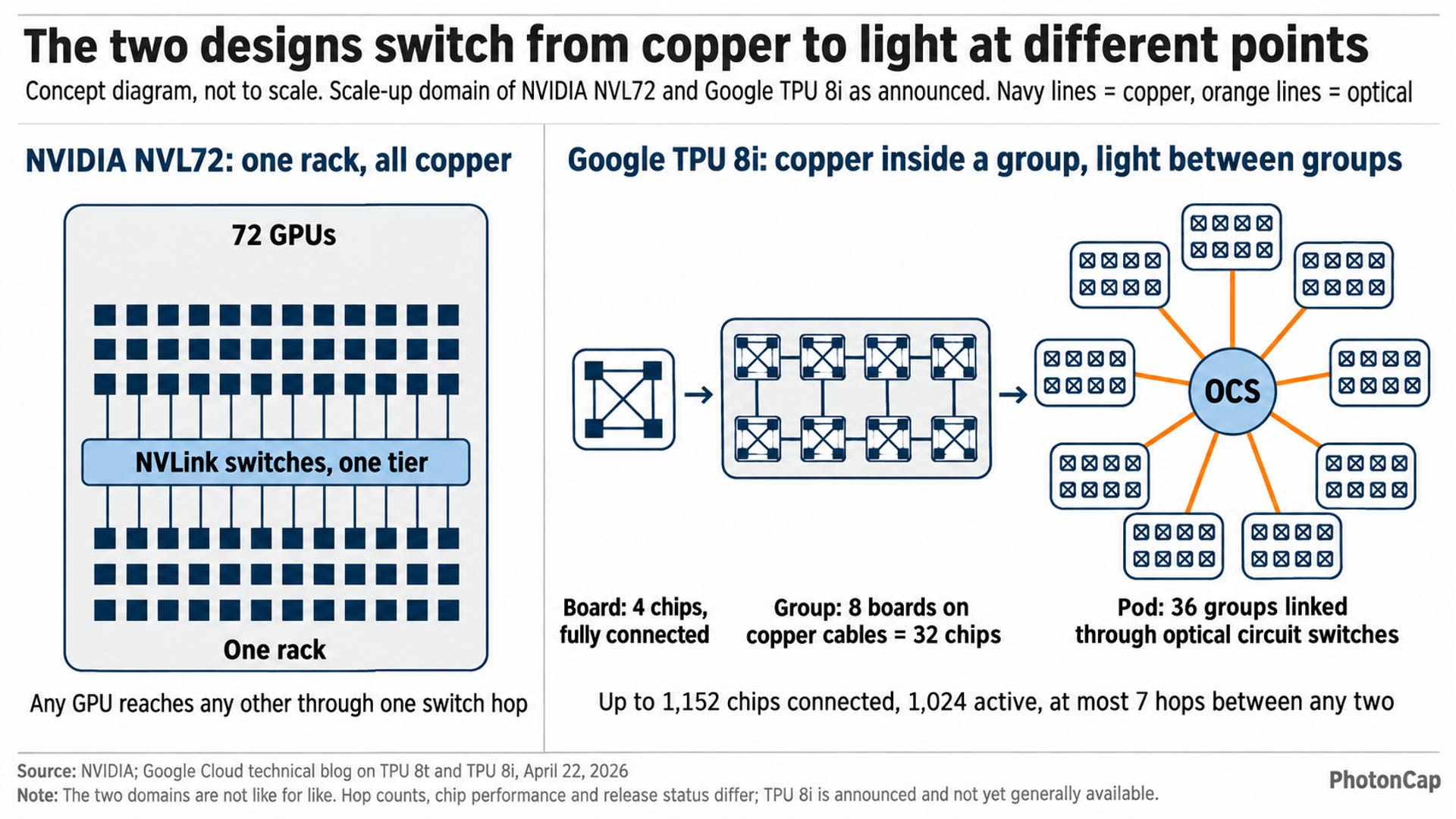
Concept diagram of where copper ends and light begins in NVIDIA NVL72 and Google TPU 8i
It would be a mistake to put 72 and 1,000 side by side as they are and read it as Google being more than ten times ahead. In NVL72 the 72 chips reach each other through a single switch hop, and Boardfly goes through up to seven. The performance of one chip differs too. You have to line up model size, response-time target, and the number of chips actually used before the comparison means anything.
Still, there is something to read here. The two companies cross from copper to light at different points. Google has operated OCS-stitched domains since earlier TPU generations, and in TPU 8i it designed the crossover to light to happen between groups of thirty-two chips. General availability of TPU 8i is still ahead. NVIDIA packed one rack full with copper, and is only now about to connect what’s outside it with light.
So when and how does NVIDIA get out of the rack? As it happens, NVIDIA gave part of that answer last month. Which boxes are still empty in the 576-chip domain? What did Marvell buy from Lumentum besides a switch? And when the domain grows, which component groups see their share grow?
