
Abstract
On July 14, UMC shipped the first mass-produced silicon photonics wafers from its 12-inch fab in Singapore [1]. The same day, Tower committed roughly $3B of its own capital to a 300mm SiPh expansion in Japan, backed by government grants [2]. Two days later, TSMC reported Q2 results: $40.2B in revenue, 67.7% gross margin, HPC at 66% of sales [3]. And two weeks before all of that, the Korean government unveiled an 8.4GW AI datacenter plan worth 550 trillion won [4][5]. When a new entrant and the incumbent leader add capacity on the same day, the question is not who loses share. The question is what demand they both see ahead. And there is a paradox on top: the more silicon photonics wins, the more InP light sources sell. This one is about $TSM, $UMC, $GFS, $TSEM, $COHR, $LITE, $MTSI, and $AXTI.
Contents
Earnings: Demand Is Still Accelerating
8.4 Gigawatts
July 14: Two Announcements, One Day
Turning Gigawatts into Transceivers
So Who Gets Hurt?
The Silicon Paradox
Scenarios
Gross margin 67.7%. Net income up 77.4%. HPC at 66% of revenue.
Those are TSMC’s Q2 numbers, out on July 16 [3]. Revenue came in at $40.2B, right at the top of the company’s own guidance of $39.0B to $40.2B, up 33.7% year over year [3]. Net income of NT$706.56B beat the LSEG consensus of NT$632.6B by nearly 12% and set a record for the fifth straight quarter [6]. Not that long ago, a foundry clearing 50% gross margin was considered excellent. At 67.7%, there is no way to read this other than demand running ahead of supply, at least on leading edge nodes.
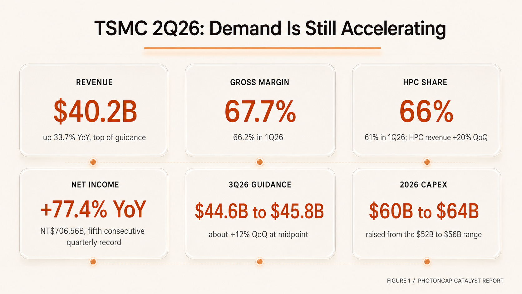
Figure 1: TSMC 2Q26 Scorecard
And that was not even the only news this week. On July 14 alone, two supply side announcements dropped. UMC and Singapore fabless SILITH shipped their first mass-produced silicon photonics (SiPh) wafers from a 12-inch fab [1], and the same day Tower announced a government backed 300mm SiPh expansion in Japan. Then there is June 29, when the Korean government said it would build 8.4GW of AI datacenters with SK, GS, and Naver by 2029 [4].
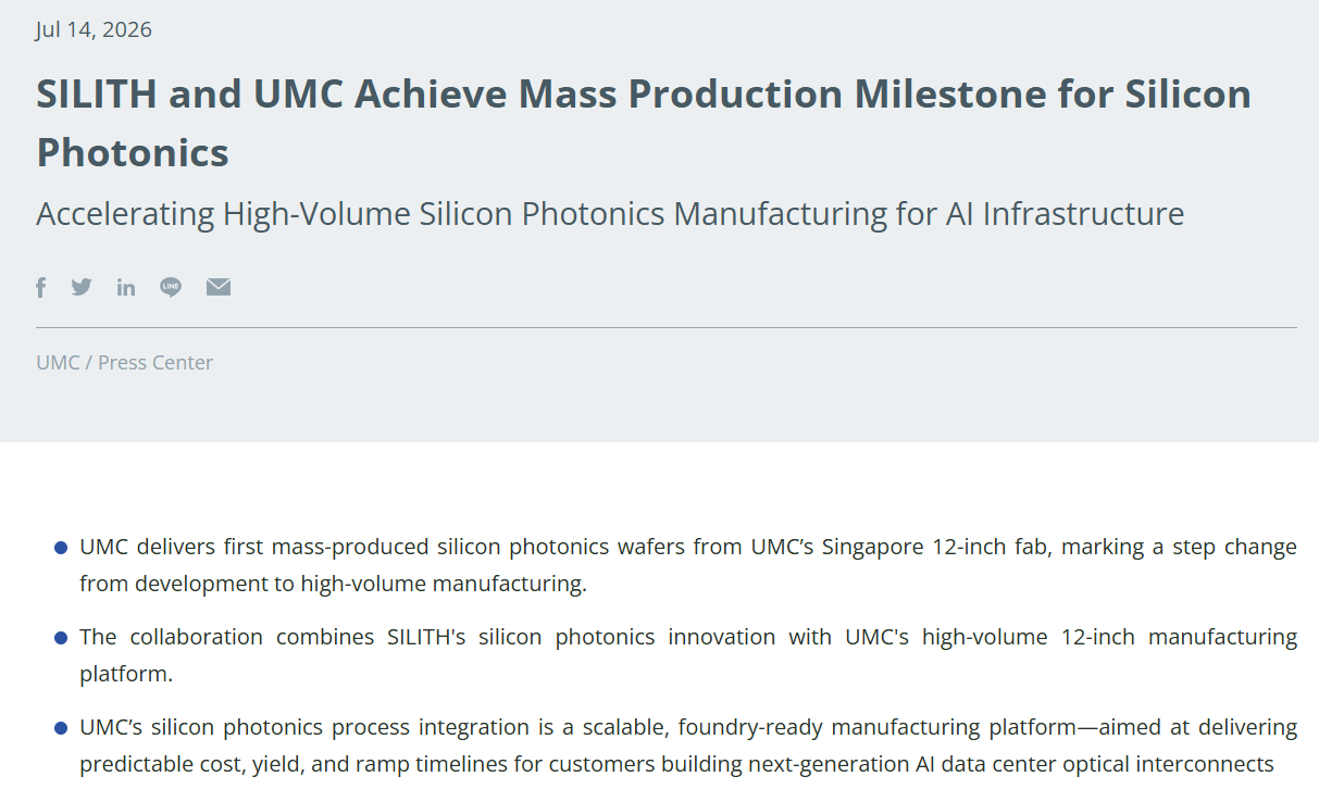
Earnings, gigawatts, and wafers.
Each one is a one day story. Put them together and a question falls out: is the market growing faster than the number of players? I think it is. And if that is right, the money is not flowing where everyone is looking.
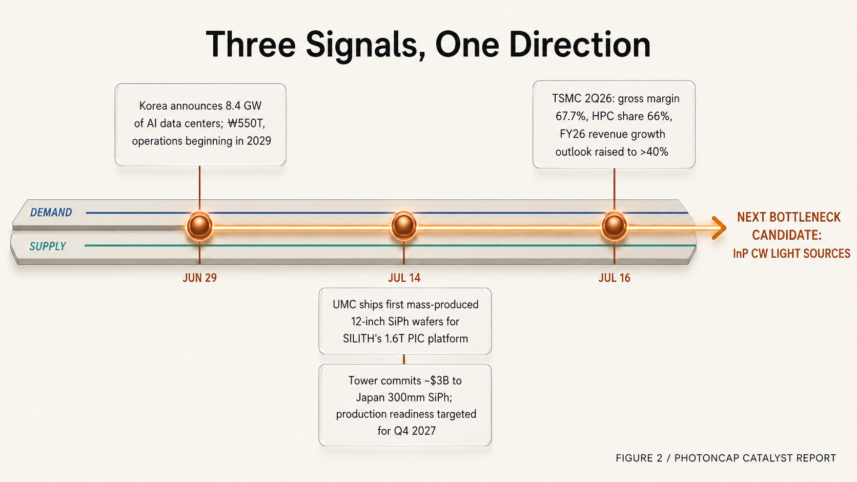
Figure 2: Three Signals, One Direction - Demand and Supply Timeline
1. Earnings: Demand Is Still Accelerating
There is no better thermometer for the AI cycle than TSMC’s results. Whether it is NVIDIA or a hyperscaler’s custom ASIC, the wafers all come out of the same place.
Put Q2 next to Q1 and the direction is obvious. HPC went from 61% to 66% of revenue, with HPC sales up 20% quarter over quarter [3][7]. Smartphone slipped to 22% [3]. Gross margin climbed again, from 66.2% to 67.7% [3][7], and this did not happen in a vacuum. The company has spent quarters warning that the 2nm ramp and overseas fab expansion would dilute margins by 2 to 3 points [7]. Absorbing all of that and still expanding margin means TSMC is getting paid that much for leading edge process and advanced packaging. By node, 2nm showed up for the first time at 3% of wafer revenue, and processes at 7nm and below made up 77% of the total [3]. There are complaints that surging memory prices are squeezing consumer and price sensitive volumes [6], but margins rising through that squeeze is exactly the point.
Guidance did not just hold. It went up. Q3 revenue guidance is $44.6B to $45.8B [3], which at the midpoint is another 12% plus quarter over quarter. On the call, management raised the full year dollar revenue growth outlook to slightly above 40% and lifted 2026 capex to $60B to $64B [3]. This is the same company that said “above 30% growth, capex at the top of $52B to $56B” back in April [7]. One quarter later, the bar moved up again. On top of that, another $100B for Arizona (cumulative $265B) to build multiple 2nm logic fabs plus advanced packaging fabs [6]. This is a company whose problem is not selling. Its problem is building fast enough.
And if wafers are selling at this pace, the bandwidth to connect those chips has to grow at the same pace. The interconnect is already moving from copper to optics.
2. 8.4 Gigawatts
Earnings are demand’s present tense. The future now gets announced in units of power.
On June 29, at a presidential office briefing, the Korean government announced a phase one plan to build 8.4GW of AI datacenters with SK (5GW), GS (2.4GW), and Naver (1GW) [4][5]. 550 trillion won. Groundbreaking in the first half of 2028, staged operation from 2029 [4][8]. In phase two, SK grows its 5GW to 15GW by 2035, taking the total to 18.4GW and cumulative investment past 1,000 trillion won [5].
If 8.4GW does not land for you, try this: it takes roughly six of the newest nuclear reactors dedicated to datacenters [4]. If the plan holds, Korea’s AI datacenter capacity reaches 14.37GW in 2030, which would be 25% of the entire Asia Pacific total of 58GW [4].
An announcement is not a groundbreaking, of course. Permitting, water, community acceptance, the risks are stacked deep. But what matters here is not whether the Korean plan is fully realized. It is that this is one piece of a global pattern. Announced AI datacenter projects worldwide total 190GW, with $5.5T of investment projected through 2030 [4]. Korea’s 8.4GW is one more light switching on inside that number. Reading gigawatts as optics demand is the same frame I used in the earlier piece on Meta’s AI infrastructure. That one was about coherent DCI between datacenters. This one is about what happens inside them.
One Layer Below SemiAnalysis’s Meta Map: Scale-Across Is Coherent, Not CPO

Over the past few months, PhotonCap has covered the supply side of the optical layer that links datacenters to one another (scale-across) three separate times. This week’s SemiAnalysis breakdown of Meta’s infrastructure is the first concrete blueprint showing that demand for that layer is being deployed at gigawatt scale.[1] The point is simple. There is not one optical fight inside an AI datacenter but two: inside the rack (scale-up) is a CPO fight, and between datacenters (scale-across) is a coherent DCI fight. Meta linking campuses up to 2,000 km apart signals that independent demand is opening for the latter, the coherent layer. It sits in exactly the distance band Marvell spells out for its own COLORZ 800 pluggable, 2,000 km at 600G and 3,000 km at 400G.[2] Tickers: $MRVL $COHR $CIEN $LITE, and on the demand side, $META.
The moment a datacenter gets announced in gigawatts, optical interconnect demand follows almost mechanically. There is a generational conversion factor between the power one GPU burns and the number of transceivers hanging off it. Below, I work through what 8.4GW means in transceiver terms.
3. July 14: Two Announcements, One Day
Against that backdrop, the supply side slipped in two quiet announcements of its own.
July 14, UMC and SILITH Technology. The first mass-produced SiPh wafers came out of UMC’s 12-inch fab in Singapore [1]. SILITH is a Singapore based SiPh fabless that builds photonic ICs (PICs) for 1.6T platforms on UMC’s 12-inch SOI process. Development to production took 18 months, and the wafers have already passed qualification at a global cloud infrastructure customer and entered volume deployment [1]. Per a Nikkei report relayed by TrendForce, SILITH’s customers include Innolight and Coherent [9], and UMC has laid out a roadmap through advanced packaging services in 2027 and an open SiPh platform in 2028 [9]. Its own 12-inch platform opens to other customers’ product development starting in 2027 [1].
Why 12-inch matters: SiPh production has long straddled 200mm and 300mm. Tower built its customer base on 200mm with PH18, while GlobalFoundries pushed 300mm Fotonix early. TSMC has been growing COUPE, a captive SiPh effort attached to its own packaging. Moving to 12-inch means more chips per wafer plus modern lithography and process control, so unit cost and uniformity improve together. In an era when transceivers ship by the millions per year, that difference goes straight to margin. Which is why this week’s two announcements also read as a declaration that the center of gravity has fully shifted to 12-inch.
The same day, Tower dropped news of its own. With support from Japan’s government (METI), it is expanding 300mm SiPh capacity in Japan [2]. Track one repurposes the Arai facility (the former Fab 6) for 300mm SiPh and advanced packaging, targeting production readiness in Q4 2027. Track two builds an additional 300mm fab next to Fab 7. Tower’s own investment is roughly $3B, net of $1B in Japanese government grants, and alongside the announcement the company raised its 2028 corporate model to $3.6B in revenue and $1.2B in net profit [2].
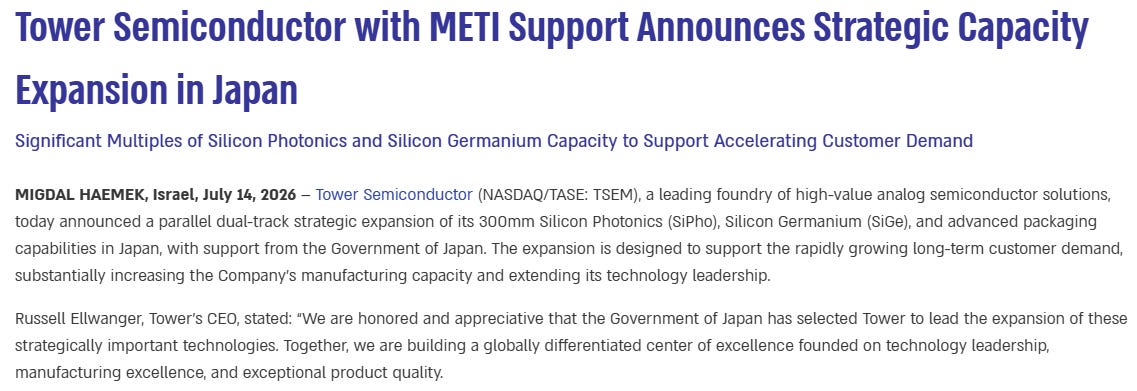
So on July 14, in a single day, the new entrant shipped its first 12-inch production wafers and the incumbent leader put $3B on 300mm. The first reaction writes itself. With this much capacity pouring in, who gets hurt?
Take the announced demand (TSMC’s 66% HPC mix, Korea’s 8.4GW, the global 190GW pipeline) and convert it into optical components. Set that in front of the four foundries and the market share frame turns out to be the wrong question. And there is one more thing. There is a third material whose demand grows the more silicon wins. Its supply chain is far narrower than SiPh foundry capacity.
