The 6 Companies Behind Coherent and Lumentum: The Real Leading Edge of the AI Optical Cycle
Aixtron, Veeco, IQE, Riber, Oxford Instruments, AXT: A Look at the III-V Compound-Semi Deposition Names
Abstract
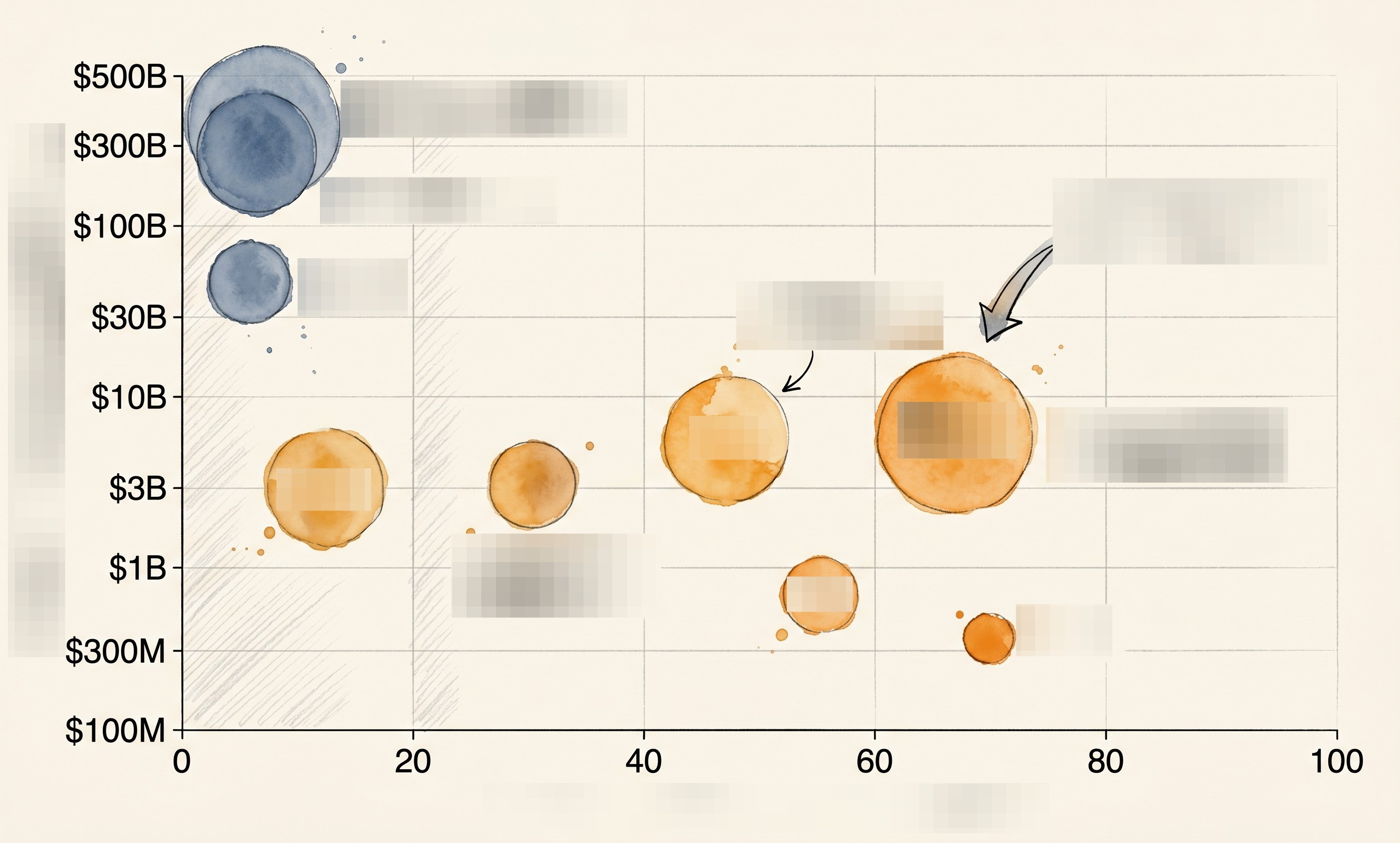
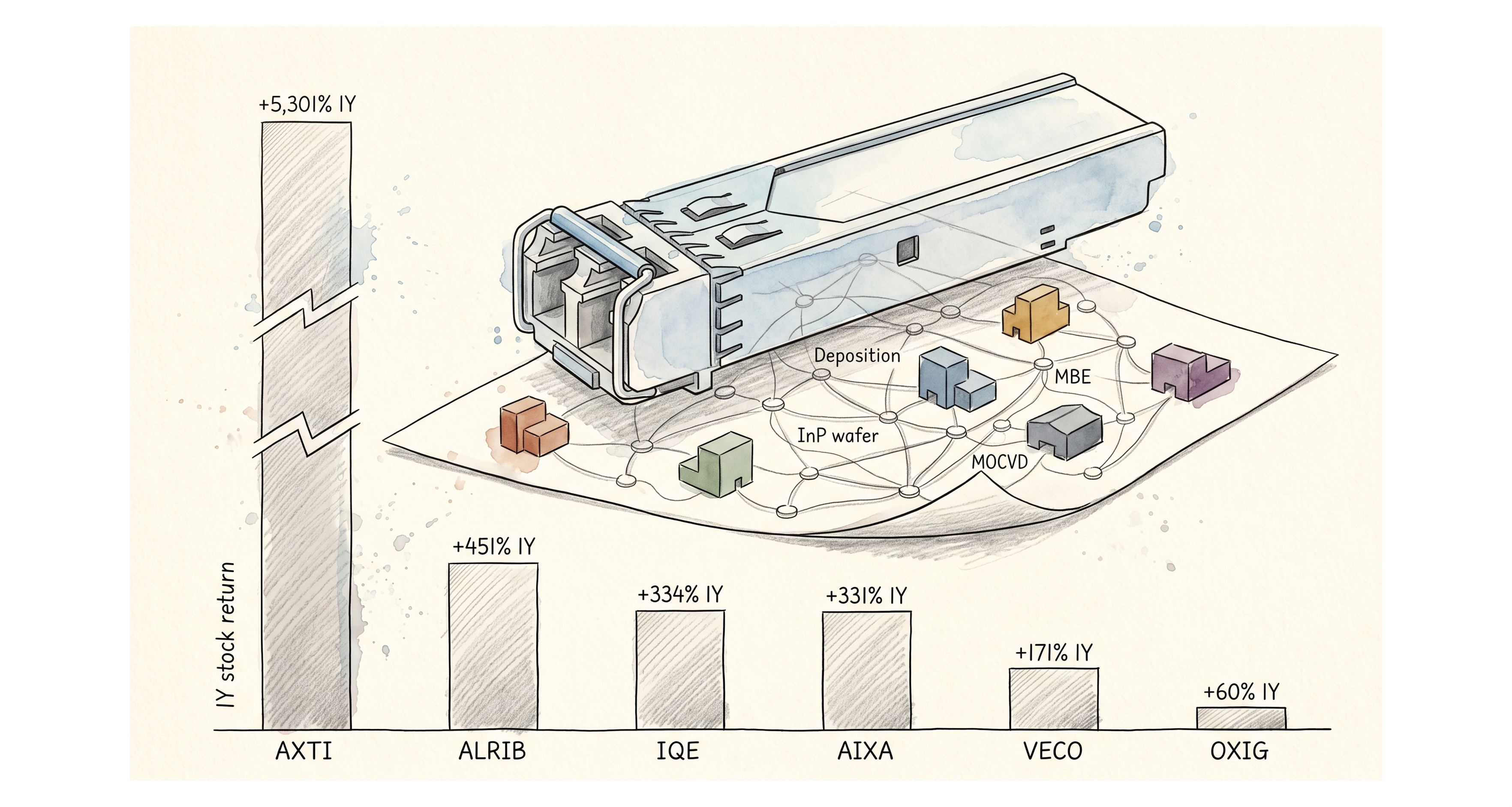
The real bottleneck of the AI data center isn’t visible at the GPU. The copper cables that move data between GPUs have hit a physical limit, so the industry is moving to light. But that light isn’t made in silicon. It’s made on III-V compound semiconductors (InP, GaAs), grown one atomic layer at a time inside what amounts to a chamber furnace. That layer-stacking job is called deposition, and the stocks of the six companies that build the deposition tools have separated by anywhere from +60% to over +5,300% over the past year. AXT roughly +5,301% (from the $2 lows to the $70-80 range), Riber about +451%, IQE about +334%, Aixtron about +331%, Veeco about +171%, Oxford Instruments about +60% (all per public market data, as of April 2026). This article walks through why this slot is the leading edge of the cycle, how the six companies differ, and where they sit relative to the large WFE (wafer fab equipment) names like AMAT and LAM. Tickers covered: $VECO, $AIXA.DE, $IQE.L, $ALRIB.PA, $OXIG.L, $AXTI. Comparison group: $AMAT, $LRCX.
Contents
Intro: Every Computing Cycle Showed Up First in “Materials”
Photonic Semiconductor Deposition, the Things You Need to Know
The 6-Company Map
Order-of-Magnitude Comparison with the Big WFE Names (paid)
Who’s Actually Making Money: Company-by-Company (paid)
Scenarios, Monitoring, and Closing (paid)
References & Sources
1. Intro: Every Computing Cycle Showed Up First in “Materials”
Step back from the noise and computing history shows the same pattern repeating. Every time a chip generation hits a physical wall, a new material steps in, and the equipment company that grows that material is the first to move and the biggest gainer in the cycle.
1990s: PC memory capacity hit a wall, DRAM jumped to new materials and processes, and the memory equipment cycle followed.
2010s: Mobile communications hit a wall, 5G needed GaAs and GaN RF, and the compound-semi RF equipment cycle followed.
Early 2020s: EVs hit a power-electronics wall, SiC and GaN stepped in, and the power compound-semi cycle followed.
Right now, in 2025-2026, the same pattern is playing out inside the AI data center. The wall this time isn’t the chip itself. It’s data movement between GPUs. NVIDIA is doubling and tripling GPU performance per generation, but for tens of thousands of GPUs to behave like one system, the cables between them have to keep up. Copper can’t. So the entire industry is shifting from electrical to optical signaling, and the parts that make light (lasers, modulators, detectors) cannot be made in silicon. They have to be grown on III-V compound semiconductors (indium phosphide InP, gallium arsenide GaAs), one atomic layer at a time, inside high-vacuum or gas-phase chambers. That layer-stacking job is called deposition.
That said, the stock-price sequence in this cycle has run in two distinct stages. The first layer to get repriced was the module companies. Coherent, Lumentum, and Innolight ramped in 2024 on 1.6T demand. Only after that did the market dig one layer deeper, asking “where is Coherent’s InP capacity coming from?”, and the question worked its way down to the deposition tool layer. AXT, Aixtron, Riber, and Veeco started getting serious re-rating only in late 2025 and into 2026. From an industrial-cycle standpoint, deposition tool orders do lead module revenue recognition (the tool has to be installed before the chip can be made). But from a stock-price standpoint, the market discovers supply chains in reverse: the most visible layer (modules) first, then digs deeper as the cycle proves out. So the asymmetry now sits not in the modules, where the rerating is mostly done, but one layer below in the deposition tool group that is still catching up.
The 1-year stock returns reflect that. Aixtron[1], the largest of the six by market cap, is up about +331% over 1 year. Riber[2], the smallest, ran roughly +451%. And the outlier, AXT[3], ran approximately +5,301% over the same window. Sorted (all per public market data, April 2026):
AXT: roughly +5,301% over 1 year (from the $2 lows to the $70-80 range). Market cap ~$4.23B
Riber: about +451%. Market cap ~$318M
IQE: about +334%. Market cap ~$628M
Aixtron: about +331%. Market cap ~$6.13B (largest of the six)
Veeco: about +171%. Market cap ~$3.1B
Oxford Instruments: about +60%. Market cap ~$2.15B
When NVIDIA announced at GTC 2025 that the Quantum-X Photonics InfiniBand switch would land later in 2025 and Spectrum-X Photonics Ethernet in 2026[4], the question of who supplies the MOCVD that grows the InP CW laser inside that switch became the question that determines these companies’ revenue visibility. The optical transceiver market itself, per LightCounting figures cited by Veeco, exceeded $23B in 2025 and grew about +50% YoY (this is the broader optical transceiver market, not an AI-only number).[5] AI capex is the single biggest driver behind that growth.
One caveat to set up. The deposition and epi tools these six companies make aren’t only mapped to AI optical. They also serve quantum computing, AR/VR display, and GaN power. The main angle of this piece is AI optical, but quantum and oxide-modulator optionality show up in places.
Core thesis: The leading slot of the AI optical cycle isn’t the module vendor at the surface, it’s the InP wafer and the III-V deposition process that grows it. The six companies that own that step are taking the most asymmetric piece of the cycle. Next-generation oxide modulators show up as a side optionality.
This article walks through Veeco, Aixtron, IQE, Riber, Oxford Instruments, and AXT, their photonic exposure, the technical edge each one carries, and how they sit relative to large WFE names like AMAT and LAM.
2. Photonic Semiconductor Deposition, the Things You Need to Know
Deposition sounds abstract, so here’s the everyday picture. Every part that emits, captures, or steers light (the laser, the modulator, the detector) is built by stacking crystalline thin films a few nanometers thick, one on top of another, with extreme precision. It’s like painting a surface one atom at a time. If a layer is off by 1nm, the laser wavelength shifts. If wafer-scale uniformity drifts by 0.5%, manufacturing yield can drop in half.
This section keeps it short on four things: (1) why InP is the core material, (2) why deposition splits into two camps (MOCVD vs MBE), (3) how back-end processing rides the same cycle, and (4) where the next generation of materials is being teed up.
2.1 Light Only Gets Made on III-V
The 1.3 and 1.55µm datacom EML (electro-absorption modulated laser) and CW DFB (continuous-wave distributed feedback) lasers that go into transceivers are mostly built on InP wafers. Silicon is an indirect-bandgap semiconductor, so it can’t generate light efficiently. 850 and 940nm VCSELs run on GaAs, and some SiPh designs use external CW lasers married to a silicon modulator, but the light source itself is still III-V.
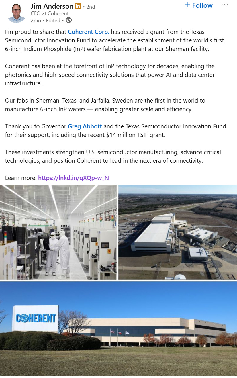
InP is the photonic-semi industry’s specialty steel. It’s hard to grow, has a small set of substrate suppliers, and scaling wafer size is painful. Coherent’s CEO said on the FY2025 earnings call that the company tripled InP capacity year over year, and even that wasn’t enough, so they brought up a new 6-inch line in Sherman, Texas.[6]
“We have tripled indium phosphide capacity year over year and expect to continue to expand capacity over the coming quarters to support the strong demand signals from our customers.”[6]
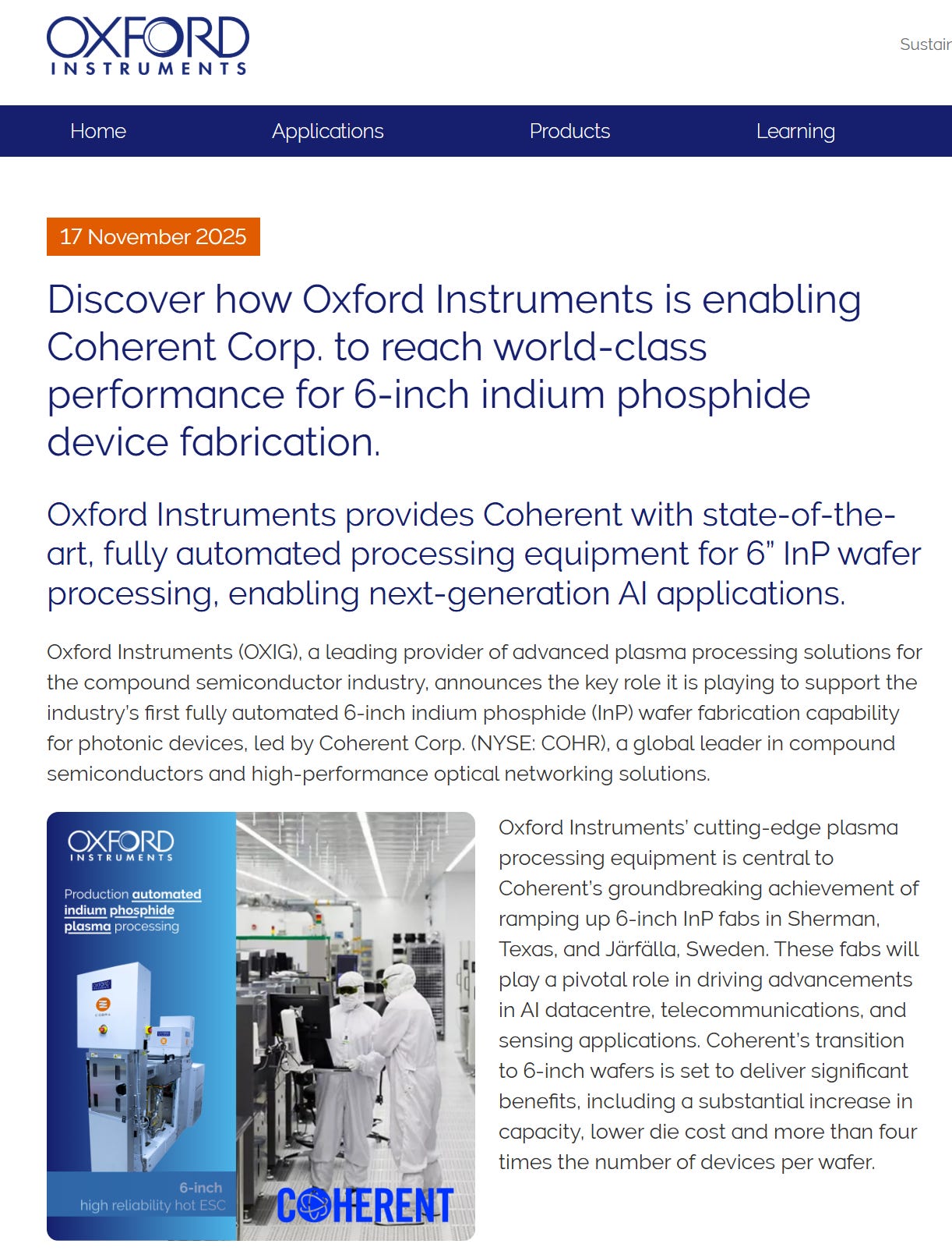
On top of the capacity story, there’s a wafer-size transition happening. InP wafers are transitioning from 4-inch to 6-inch in earnest, with 8-inch on the longer-term roadmap. The core of the current cycle is the 6-inch ramp. Pure area math says 4-to-6-inch is about 2.25x, but Coherent’s March 2024 announcement of its 6-inch InP fab framed the combined effect of edge exclusion, automation, usable area, and yield improvement as “4x the number of devices per wafer” with a “greater than 60% reduction in die cost”[7]. Oxford Instruments’ November 2025 release describes the same effect as “more than four times”[8]. Each time the industry transitions to a larger wafer size, the existing 4-inch-centric process toolset isn’t enough on its own, and new investment in tools matched to the larger wafer size and full automation is required. That sizing transition is itself a multi-year new-investment cycle for the deposition vendors.
AXT’s InP backlog has cleared a record $60m, and Q3/2025 InP revenue ran +250% QoQ.[9] In April 2026 the company raised $550m specifically to expand capacity.[3] An $88m revenue company raising $550m more isn’t being treated by the market as a temporary supply hiccup. AXT’s InP substrate business and its position in the AI optical supply chain were covered in detail in a prior PhotonCap piece.[10]
Related Articles about InP:
AXT Inc. (AXTI) Deep Dive: The Hidden Bottleneck in AI Optical Interconnects

1. The Hook: Why Pay Attention to Indium Phosphide (InP) and AXT Inc. Now?


2.2 Two Branches of Deposition: MOCVD and MBE
Two pieces of equipment dominate InP epi wafer production. The names are jargon, so here’s the quick mental model.
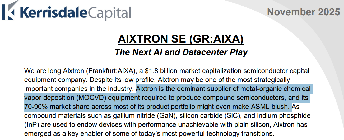
MOCVD (Metal-Organic Chemical Vapor Deposition) flows precursor gases over the wafer in a chamber to grow thin films. It has high throughput and can process several wafers in a single run, which makes it the default for volume manufacturing. Almost all AI optical InP lasers are grown on MOCVD. The market is essentially Aixtron and Veeco, with Aixtron’s share of advanced photonic MOCVD running in the 70-90% range.[11]
MBE (Molecular Beam Epitaxy) grows films one atomic layer at a time inside an ultra-high-vacuum chamber. Throughput is lower than MOCVD, but precision is much higher, which makes it the workhorse for quantum dot lasers, quantum-computing qubit stacks, and oxide ferroelectric films like BTO and STO. The global leader in production-scale MBE is Riber, with Veeco present through the GEN platform.
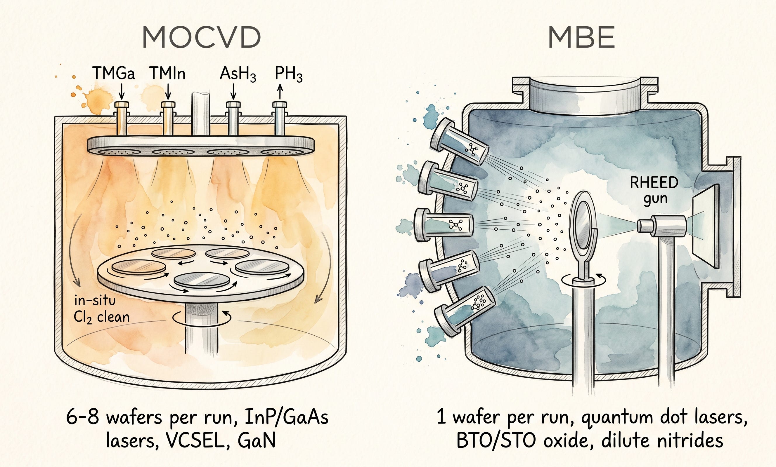
[Figure 1: MOCVD vs MBE chamber comparison]
Here’s the important part. The traditional split (MOCVD for volume, MBE for precision niche) is breaking down in 2026. Veeco delivered the first unit of a 300mm silicon-compatible BTO MBE cluster system, co-developed with imec.[12] What used to be Riber’s territory (oxide MBE) now has Veeco entering it through an imec partnership, with the explicit goal of volume manufacturing for next-generation datacom modulators. From a stock perspective this is a meaningful signal, and the paid section unpacks it.
2.3 Back-End Processing Rides the Same Cycle
An epi wafer alone isn’t a chip. Sub-100nm features have to be patterned for waveguides and gratings, passivation has to be deposited, and laser facets have to be mirror-coated. The dominant player in this back-end stack for InP and GaAs is Oxford Instruments. OIPT (Oxford Instruments Plasma Technology) is the supplier of the core plasma processing equipment ramping in Coherent’s Sherman and Järfälla 6-inch InP fabs.[8]
OIPT’s photonic-semi product family runs across PlasmaPro 100 Cobra (ICP-RIE for waveguide and ridge etching), ICPCVD (low-temperature SiN/SiO2 passivation), OpAL/FlexAL ALD (atomic-layer dielectrics), and Ionfab IBE (ion-beam etching for laser facet mirror coating). A photonic-semi production line isn’t a single MOCVD tool, it’s a multi-step stack: MOCVD/MBE (deposition) + ICP-RIE (etch) + ICPCVD (passivation) + ALD (dielectric) + IBE (mirror coating). Each step has a near-monopoly supplier, and when AI optical capacity scales, the whole stack scales with it.
2.4 The Next-Gen Material Is the Hook
Everything above is the current cycle. The next generation gets more interesting. Oxide ferroelectric thin films like BTO (BaTiO3, barium titanate) are emerging as the leading candidate for the next-gen modulator inside SiPh transceivers. BTO has a strong electro-optic effect that silicon doesn’t, and Veeco’s imec partnership built a hybrid MBE system that can grow it on a 300mm SiPh-compatible platform at production-relevant cost.[12] imec’s framing of the opportunity has the datacom transceiver market growing from $2.9B in 2024 to $13.1B in 2030, with BTO modulators among the largest beneficiaries.[12]
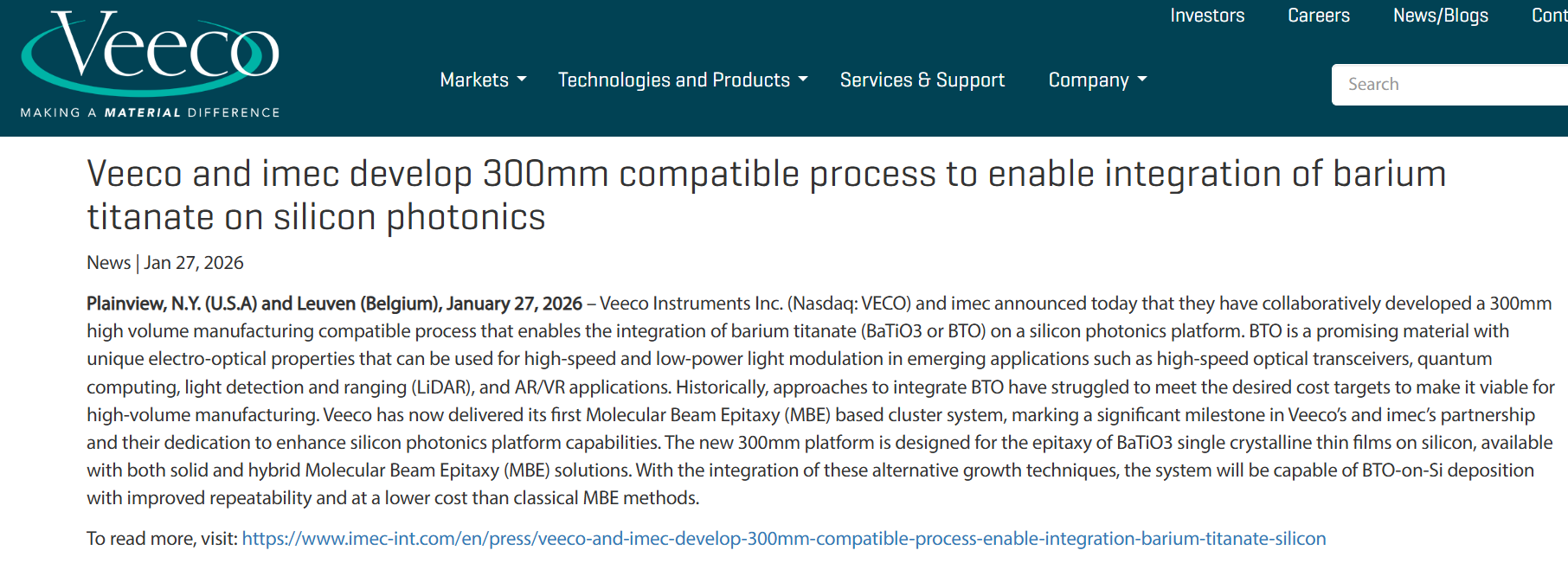
Riber is in the same area with the ROSIE platform, which sets up a head-to-head competition between the two companies. That dynamic is one of the biggest stock variables for the next 12-18 months. So who’s locked in the first orders, and who’s getting credit for the second variable, the quantum-computing hybrid materials angle? That’s what the paid section walks through.
Section takeaway: AI optical looks like a transceiver story on the surface, but the real bottleneck is the InP laser chip inside, and that chip is built by the full deposition-plus-etch stack: MOCVD/MBE, ICP-RIE, ALD, IBE. Next-generation BTO oxide modulators are an R&D-stage push toward volume, with Veeco-imec and Riber on a direct collision course over SiPh foundry adoption.
3. The 6-Company Map
3.1 Six Photonic-Semi Deposition Companies
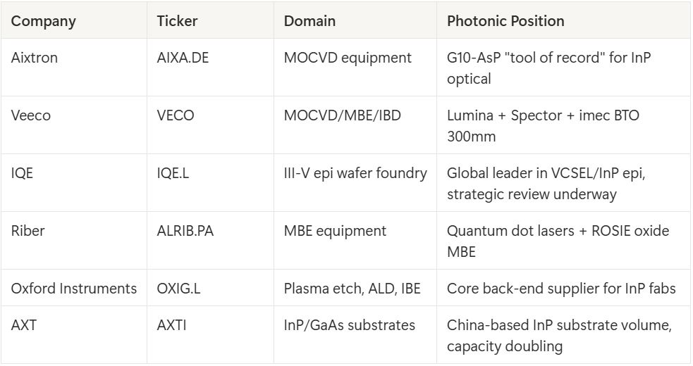
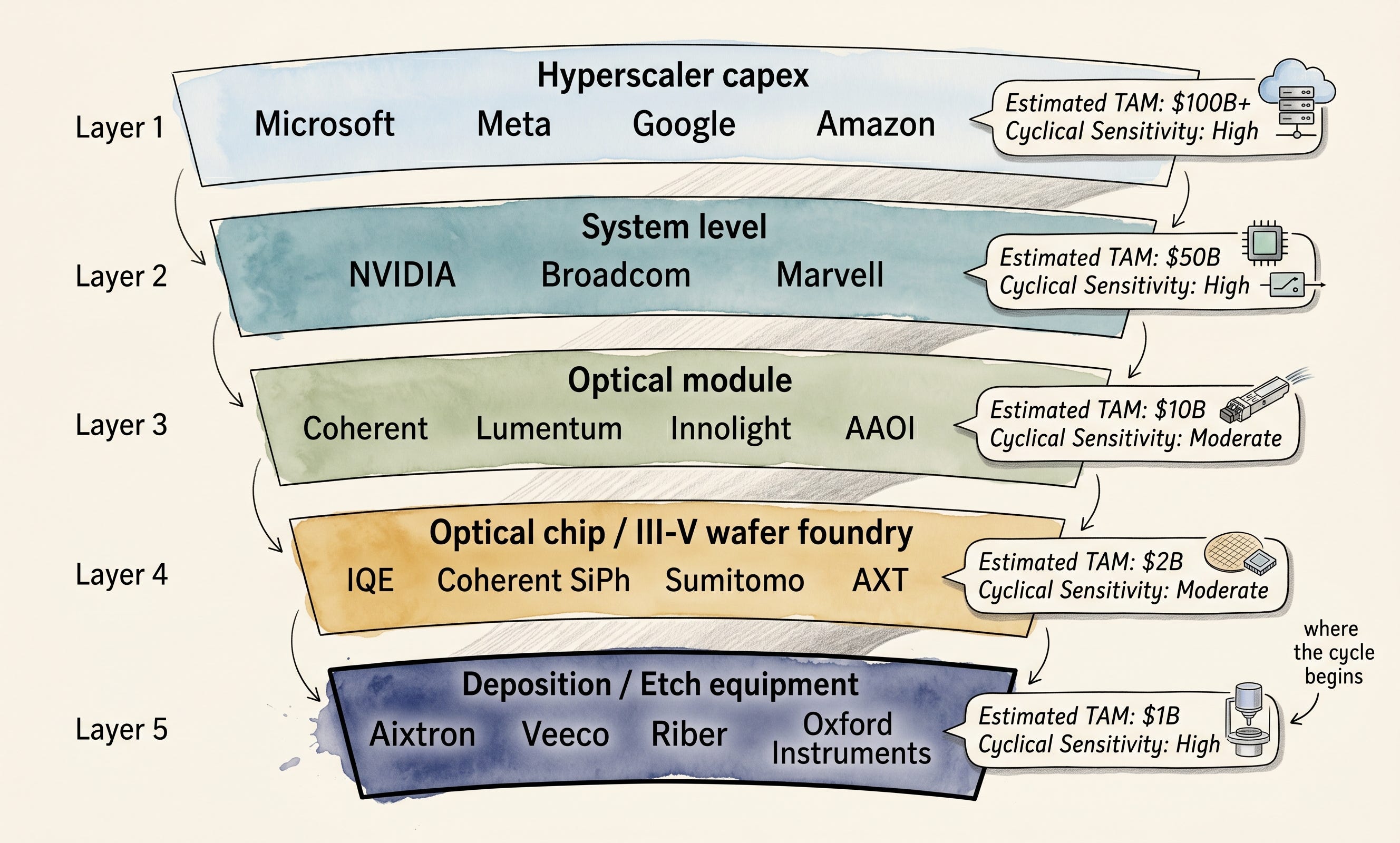
[Figure 2: AI optical supply chain layers and the 6 companies]
3.2 Where the Real Differences Start: Past the Paywall
What’s covered up to this point is everything that public sources will give you. The real difference starts past this line. The six companies are all riding the same cycle, but they split cleanly into “already converted into backlog,” “still trading on option value alone,” “ran ahead of the fundamentals,” and “tied to an M&A outcome.” And there’s one more hidden card sitting inside the cycle: Veeco-imec’s BTO 300mm move into what was Riber’s standalone territory, and the question of which commercial MBE platform actually maps onto Microsoft’s Majorana 1 quantum chip (the topological-qubit quantum processor unveiled in February 2025) and its InAs+Al hybrid stack. Those two are the core variables for the most asymmetric positions over the next 12 months. Below, we walk through why the six companies generate an order-of-magnitude different beta versus the big WFE names like AMAT and LAM, then go company by company on what to watch over the next 12 months, separating the riskiest name from the cleanest beneficiary.
Section takeaway: Six companies are riding the same cycle, but the technical weapons and business models are different. That difference splits them into four distinct groups, and two hidden variables drive the next 12 months of positioning.
4. Order-of-Magnitude Comparison with the Big WFE Names
The natural follow-up question. Are Applied Materials, LAM Research, and ASMI plugged into SiPh?