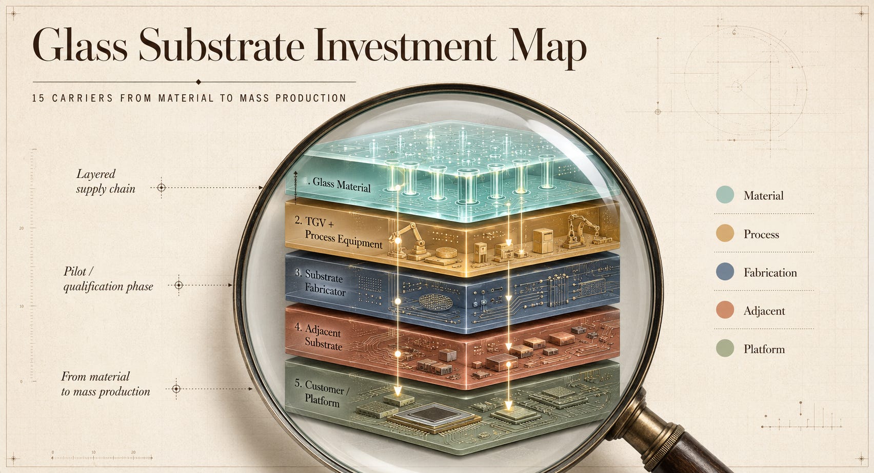
[Investment Map] 15 Companies in the Glass Substrate Cycle: From Material to Mass Production
$NVDA $AMD $INTC $TSM $GLW + 14 more: 15 Carriers from Material to Mass Production


For the past 30 years, high-performance CPU/GPU package substrate stacks have been built almost entirely on organic build-up substrates, specifically ABF (Ajinomoto Build-up Film) variants. 2026 is the first year glass substrates cross from R&D into pilot/qualification phase. Intel has committed to a “second half of this decade” production window [1], TSMC is reportedly preparing its CoPoS pilot line for mid-2026 completion [2], and Absolics has entered AMD certification at its Georgia Covington fab [3]. This article evaluates 15 publicly traded companies across six countries using a glass-substrate-specific GVM Score (5-axis framework), maps them to a 4-tier cascade, and distributes them across a 12-month Catalyst Calendar. Identification, mapping, and scenario analysis for all 15 companies are covered in the paid section.
This article was prepared in collaboration with Nutty and Damnang. The GVM Score is a framework I built for my own investment decisions. Of the 15 companies analyzed, I held existing positions in 3 before writing, and initiated positions in 2 additional companies immediately after constructing the GVM table. Which companies those are is disclosed inside the article.
Contents
Intro: The Substrate Is Changing for the First Time in 30 Years
Technical Background: Organic vs Glass, and TGV
Why the Cycle Starts Now
Multiple Applications on the Same Supply Chain
GVM Score, Cascade Sequencing, Catalyst Calendar
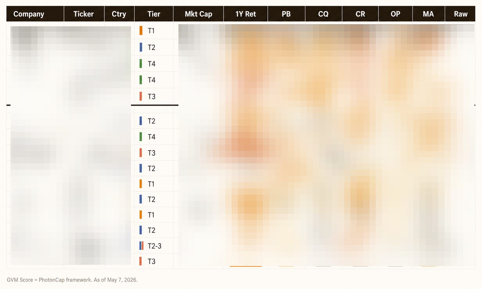
15 Carriers: Company Identification + Market Cap Comparison
GVM Score: Glass-Substrate-Specific 5-Axis Evaluation
Cascade Sequencing: Time-Lag Between Tiers
Catalyst Calendar: Trigger Events Over the Next 12 Months
Company Cards: Top 5 Deep + 10 Compact
Asymmetric Outcome: Scenarios and Monitoring
Where the Framework Breaks: Validation Signals by Hypothesis
Watchlist: Unlisted + Adjacent
Conclusion: The Substrate Timeline Mismatch
References & Sources
1. Intro: The Substrate Is Changing for the First Time in 30 Years
One-year returns. +850%. +675%. +554%. +341%. +328%. These are stocks sitting on the glass substrate supply chain. The lowest of the 15 still returned +10%. Over the same period, SMH (semiconductor ETF) returned roughly +30%. Which companies these are unfolds in this article.
For 30 years, the substrate stack underneath high-performance CPUs, GPUs, and server accelerators has been built mostly on organic build-up substrates, particularly ABF. 2026 is the first year glass substrates cross from R&D into pilot/qualification phase. Volume ramp follows in 2027 to 2030.
The physics make sense. AI accelerator packages now exceed 100mm x 100mm, and organic substrates cannot handle the warpage. CTE (coefficient of thermal expansion) mismatch with silicon causes cracking under thermal cycling. Glass can be CTE-matched to silicon, has an order of magnitude lower dielectric loss, and can be processed in large panels [4].
But the problem is not just one material. When one layer of the substrate stack changes, every process above and below it changes too. Desmear equipment built for organic, laser drilling built for organic, plating built for organic, inspection built for organic. All of it has to be rebuilt for glass. Fifteen companies sit at the chokepoints of this cycle. They span South Korea, Japan, Germany, the United States, Taiwan, and Austria. Market caps range from $483M to $157B, a 325x spread, yet all of them are exposed to the same cycle.
Core thesis: The AI accelerator substrate transition from organic build-up to glass begins with a 2026 pilot/qualification phase and extends into a 2028 to 2030 volume ramp window. Cycle alpha is not captured by generic financial metrics (margin, valuation) but by five glass-substrate-specific axes: process bottleneck control, customer qualification depth, capex recovery visibility, order pipeline depth, and multi-application readiness.
This article covers 15 publicly listed companies exposed to the production cycle, an unlisted watchlist, and Chinese competitor developments.
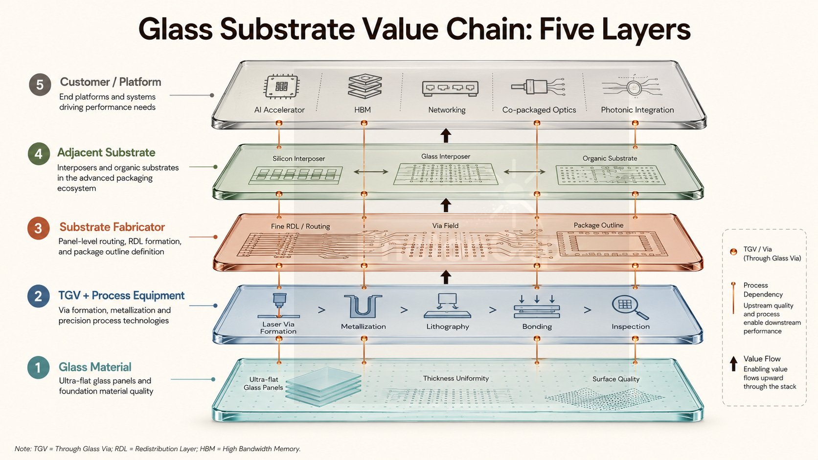
[Figure 1: Glass substrate value chain / 5-layer schematic, no company names]
2. Technical Background: Organic vs Glass, and TGV
To understand why glass substrates replace organic in one view, look at three dimensions.
First, flatness and warpage. Organic resin warps in large packages. As AI accelerator die areas exceed the reticle limit (858mm²) into 2-reticle and 3-reticle territory, organic substrates face increasing warpage, interconnect reliability degradation, and joint crack risk under thermal cycling. Glass has an order of magnitude lower surface roughness and near-constant warpage behavior [4].
Second, dielectric properties and signal integrity. When AI accelerators run SerDes above 100GHz, substrate dielectric loss converts directly into wasted power. Glass has an order of magnitude lower dielectric loss than organic, delivering the same bandwidth at lower power [4].
Third, panel-level processing. Silicon interposers are wafer-based, limited to 300mm. Glass can be processed in large panels (e.g., 510mm x 515mm), offering several times more usable area than a 300mm wafer. This is why TSMC is pursuing CoPoS (Chip-on-Panel-on-Substrate) [2].
But glass has one big problem. You cannot drill vias through it. More precisely, you cannot mechanically drill glass like organic or plasma-etch it like silicon. Glass is brittle. A single micro-crack kills yield immediately.
This is where a new process category emerged. TGV (Through-Glass Via) processing. A laser selectively weakens a zone inside the glass, then a chemical etch removes only that zone to form a clean via. LIDE (Laser-Induced Deep Etching), LMCE, femtosecond laser processes, and other variants all fall into this category [5].
The cycle’s bottleneck shows up in TGV and metallization before it shows up in raw glass panels. The number of companies worldwide that can build TGV drilling equipment can be counted on one hand. The same goes for the RDL (redistribution layer) lithography and bonding equipment that follows the drill. This is why small-cap companies receive large beta in this cycle.
Supply chain layers:
Glass material layer: global glass panel makers (3 listed + Schott AG, unlisted)
TGV + process equipment layer: via drilling, RDL lithography, bonding, and inspection equipment makers
Substrate fabricator layer: companies producing finished glass substrates for customers
Adjacent substrate layer: incumbent organic substrate leaders exposed to the glass transition
Customer / Platform layer: Intel, TSMC, AMD, NVIDIA, Broadcom
Layer 2 is critical. It is not just TGV drilling. After via formation comes metallization (seed layer + plating), RDL patterning (lithography), glass-to-glass bonding, and inspection. Watching only the TGV drilling equipment maker means missing half of Tier 2. (A separate deep-dive on the leading TGV equipment company in this cycle is available in The Glass Beneath AI Chips.)
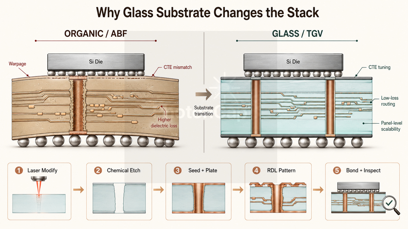
[Figure 2: Organic vs Glass substrate cross-section / TGV process flow (drilling, metallization, RDL, bonding, inspection)]
For a deeper look at the equipment and platform positions in the glass substrate value chain, see
The Glass Beneath AI Chips: The +255% YTD Equipment Stock Behind the EIC-to-CPO Packaging Shift

The packaging substrate for AI accelerators is beginning to shift from organic to glass. This transition is already underway in EIC (Electronic IC) packaging. As it extends to CPO (Co-Packaged Optics) and EPIC (Electronic-Photonic IC), glass becomes not just “a better alternative” but the most compelling platform among currently available options. This article focuses on the equipment and integrated platform positions in the glass substrate value chain, maps the current positioning of glass material and substrate makers, and examines the complementary relationship between glass packaging and Photonics-SOI demand. Key numbers: the leading equipment stock in the glass substrate cycle is up
For the full picture of why AI accelerator power density is reshaping packaging architecture, from grid to transistor across six orders of magnitude in voltage, see Nutty's article:

3. Why the Cycle Starts Now
Glass substrate R&D has been running for over a decade. Intel has had its ATTD (Assembly and Test Technology Development) team working on glass substrates since 2014 [6]. So why is 2026 the inflection point? Three triggers landed in the same quarter.
First, Intel’s production commitment. After the September 2023 announcement, the market doubted Intel’s follow-through. A rumor circulated in mid-2024 that Intel had abandoned glass substrates [7]. Then Intel reaffirmed the commitment in September 2025, and at NEPCON Japan in January 2026, it demonstrated a thick-core glass substrate combined with EMIB [8]. The package measured 78mm x 77mm, roughly 1,716mm² (2 x 858mm²) of silicon area. That is a package exceeding a single reticle limit.
Second, TSMC’s CoPoS acceleration. TSMC had been constrained by organic substrates in its CoWoS architecture. Starting in late 2025, TSMC pulled forward the CoPoS (Chip-on-Panel-on-Substrate) roadmap. The CoPoS pilot line is reportedly targeted for mid-2026 completion. Volume production expectation is 2028 to 2029 [2]. As NVIDIA Rubin/Blackwell architectures are increasingly likely to sit on CoPoS, glass demand will absorb a portion of existing organic substrate maker backlogs at some point.
Third, Absolics AMD sampling. As of January 2026, Absolics had completed major equipment installation at its Georgia Covington fab and began supplying mass-production samples to AMD [3]. Korean reporting indicates that the exclusive TGV contract with F&S Electron expired in March 2026, and Absolics is transitioning to dual sourcing [9]. This signals a shift from R&D samples to customer qualification and early commercial sampling.
These three triggers landing simultaneously led the market to frame 2026 to 2027 as the “qualification phase” and 2027 to 2028 as the start of high-volume manufacturing [10].
Two caveats. First, this cascade may not be sequential. If hyperscalers place simultaneous orders at Tier 2 and Tier 3 without waiting for lag, the sequential cascade turns into a parallel ramp. This is a key validation point in the paid cascade analysis.
Second, the P in CoPoS does not necessarily mean glass. TSMC’s official language is “large-area panel.” The initial panel could be a continuation of silicon interposer or glass substrate. Whether glass wins on cost efficiency for panel substrates, or silicon returns in a large panel format, is the single biggest fork in the cycle thesis.
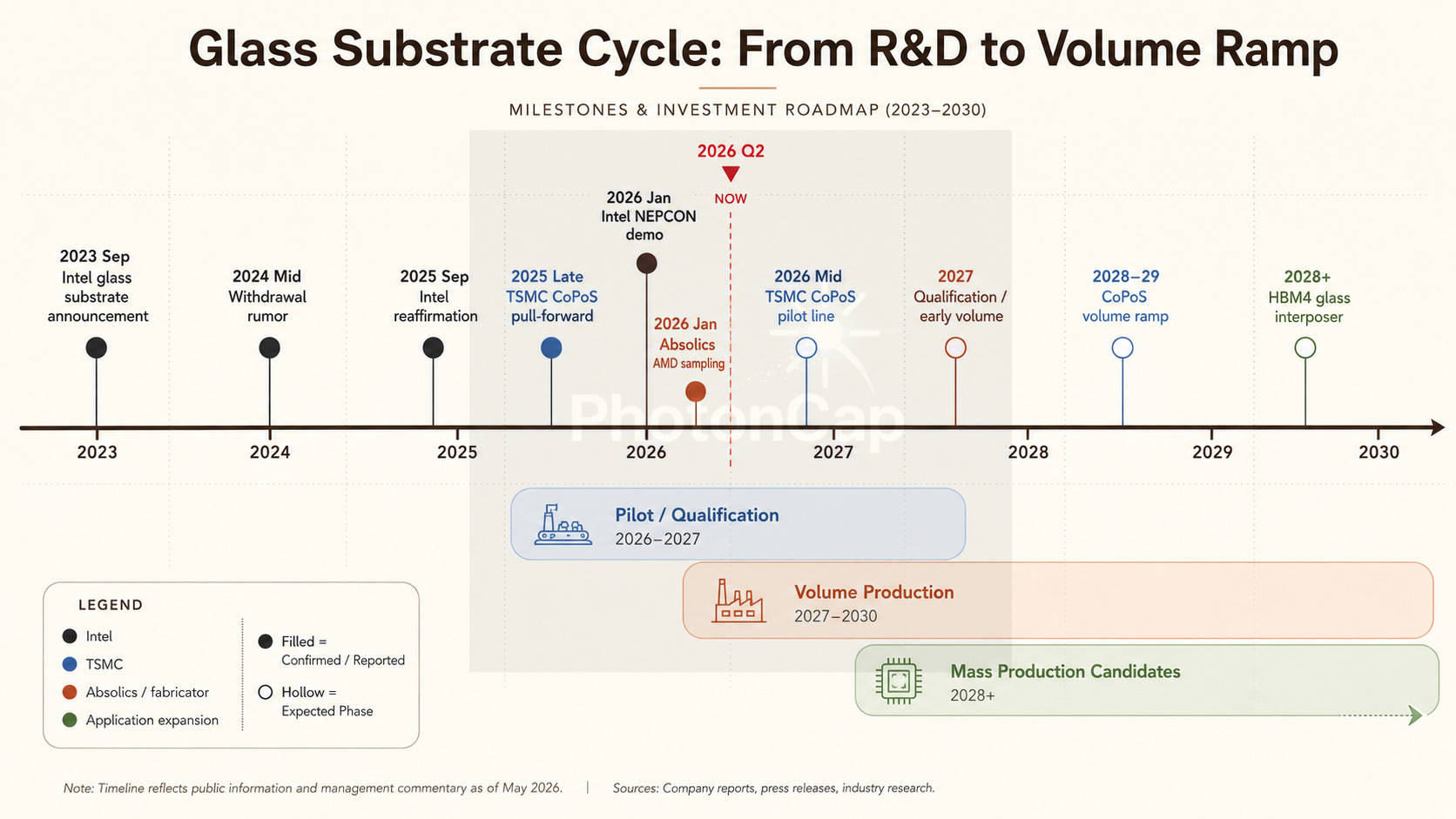
[Figure 3: Glass substrate cycle timeline / 2023 to 2030]
4. Multiple Applications on the Same Supply Chain
Looking at the glass substrate cycle through only one application, AI accelerator substrates, makes the picture too small. At least three more applications are queued on the same TGV processes, the same panel processing infrastructure, and the same glass panels.
HBM4 glass interposer. HBM currently sits on silicon interposers. For HBM4, stack height, warpage, interposer routing density, and thermal-mechanical reliability are all simultaneously critical. Glass has lower thermal conductivity than silicon, so its adoption logic is not heat spreading superiority but rather CTE tuning, flatness, low-loss routing, and panel scalability [10]. Market participants are discussing HBM4 glass interposer adoption beginning in 2028.
Co-Packaged Optics (CPO). CPO places optical transceivers within sub-millimeter distance of a switch ASIC. Glass opens the door to processing electrical RDL and optical waveguides on the same substrate, and is discussed as a platform with potential advantages in cost, panel scalability, and assembly yield relative to silicon photonics interposers [13]. CPO commercial deployment discussions are expected to accelerate from 2026 to 2027, but mainstream production of glass-based integrated electro-optical substrates may come later.
Photonic integration. Mounting both EIC (Electronic IC) and PIC (Photonic IC) on a single package is the next stage. A glass interposer carrying both EIC and PIC could bring optical fiber connectivity all the way into the substrate. Production is further out, but first commercial products are possible between 2028 and 2030 [13].
These three applications queued on the same glass supply chain have one implication. Even if the AI accelerator substrate cycle cools, the glass supply chain passes the baton to the next application. This is a multi-application supply chain cycle, not a single-application one.
This is the biggest difference from the optical semiconductor deposition cycle. That cycle’s beta was driven by a single application, optical communications, and when the application cycle cooled, the beta faded with it. Glass substrates have applications queued, which extends supply chain duration.
Key takeaway: The glass substrate supply chain is a multi-application supply-chain beta, not a single-application cycle. AI accelerator substrates are the first application. HBM4 interposer, CPO, and photonic integration are queued next.
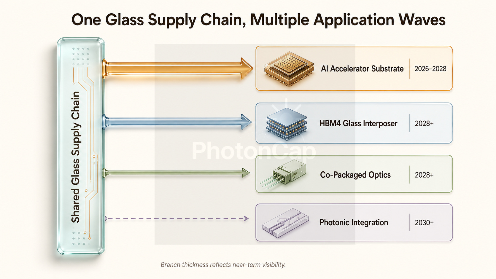
[Figure 4: Multi-application supply chain stack on glass substrate]
5. GVM Score, Cascade Sequencing, Catalyst Calendar
The market has been evaluating the glass substrate cycle using generic financial metrics: margin, valuation, P/E. But when a cycle is crossing from R&D into commercialization, generic metrics misjudge it. Alpha in the glass substrate cycle resolves across five axes: process bottleneck control, customer qualification depth, capex recovery visibility, order pipeline depth, and multi-application readiness. The evaluation dimensions are not revenue share or ASP times volume, but how far yield has progressed, how deep customer certification runs, and whether capex can be recovered.
The paid section applies three frameworks simultaneously to all 15 companies.
Framework 1: GVM Score (Glass Value-chain Maturity, 5-axis). Each company is scored 1 to 5 on five dimensions. Raw total ranges from 5 to 25. The five axes are Process Bottleneck, Customer Qualification, Capex Recovery, Order Pipeline, and Multi-App Readiness. What exactly each axis measures, how 1-point differs from 5-point, and how phase weighting shifts the ranking are covered in the paid section.
Framework 2: Cascade Sequencing (4-tier with time-lag). The glass cycle is not a single tier. Tier 1 (Material) feeds Tier 2 (Equipment) feeds Tier 3 (Fabricator) feeds Tier 4 (Adjacent/Customer), with 6 to 12 month lags at each step. Where we are now determines alpha.
Framework 3: Catalyst Calendar (catalyst event timeline). Catalyst events expected within 12 months are plotted on a timeline, identifying which company’s catalyst lands when.
Everything up to this point is visible from public information alone.
The real differentiation starts here. How each of the 15 companies scores on five axes, and how rankings shift when phase weighting is applied. Where the valuation gap sits across the four tiers. There is a GVM top-tier company that the market still prices as an organic stock rather than a glass substrate stock. And there is a mid-tier company on raw score whose ranking jumps when phase weighting is applied.
One market inefficiency stands out. A GVM top-tier company is being priced by the market purely on organic stock multiples, producing the widest price spread within its GVM cluster. Which company that is unfolds in the paid section.
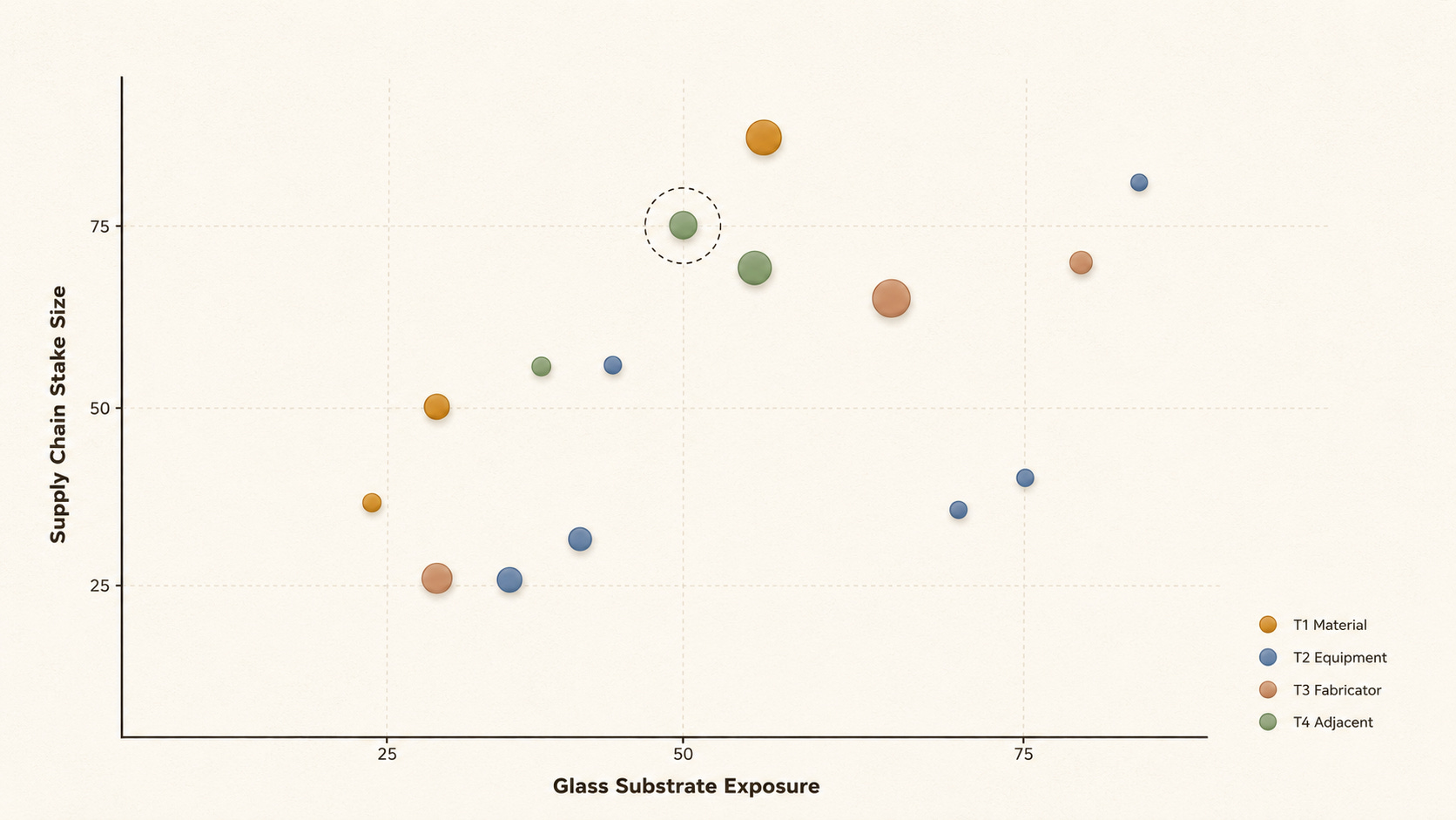
[Figure 5: Glass substrate cycle positioning matrix / Y-axis stake size, X-axis substrate exposure, no company names]