
The Glass Beneath AI Chips: The +255% YTD Equipment Stock Behind the EIC-to-CPO Packaging Shift
How Glass Substrates Are Reshaping Packaging from EIC to CPO, and the Investment Chokepoints That Matter

The packaging substrate for AI accelerators is beginning to shift from organic to glass. This transition is already underway in EIC (Electronic IC) packaging. As it extends to CPO (Co-Packaged Optics) and EPIC (Electronic-Photonic IC), glass becomes not just “a better alternative” but the most compelling platform among currently available options. This article focuses on the equipment and integrated platform positions in the glass substrate value chain, maps the current positioning of glass material and substrate makers, and examines the complementary relationship between glass packaging and Photonics-SOI demand. Key numbers: the leading equipment stock in the glass substrate cycle is up +255% YTD, while the glass core substrate market is estimated to grow from $244M in 2024 to ~$460-586M by 2030 according to Yole and QY Research estimates.
Contents
Intro: What YTD +255% Is Telling Us
Technical Context: Why Glass Is Needed (EIC, CPO, EPIC)
Three Layers of the Value Chain, One Complement, and Two Hidden Cards
Glass Substrate Majors
Watchlist + Photonics-SOI Complement
Monitoring Points + Closing
References & Sources
1. Intro: What YTD +255% Is Telling Us
LPKF Laser & Electronics (LPKFF / LPK.DE). A 50-year-old industrial laser equipment company headquartered in Garbsen, Germany. Annual revenue of €115M (FY2025), market cap roughly €481M. Its stock is up 255% year-to-date in 2026. [1][2]
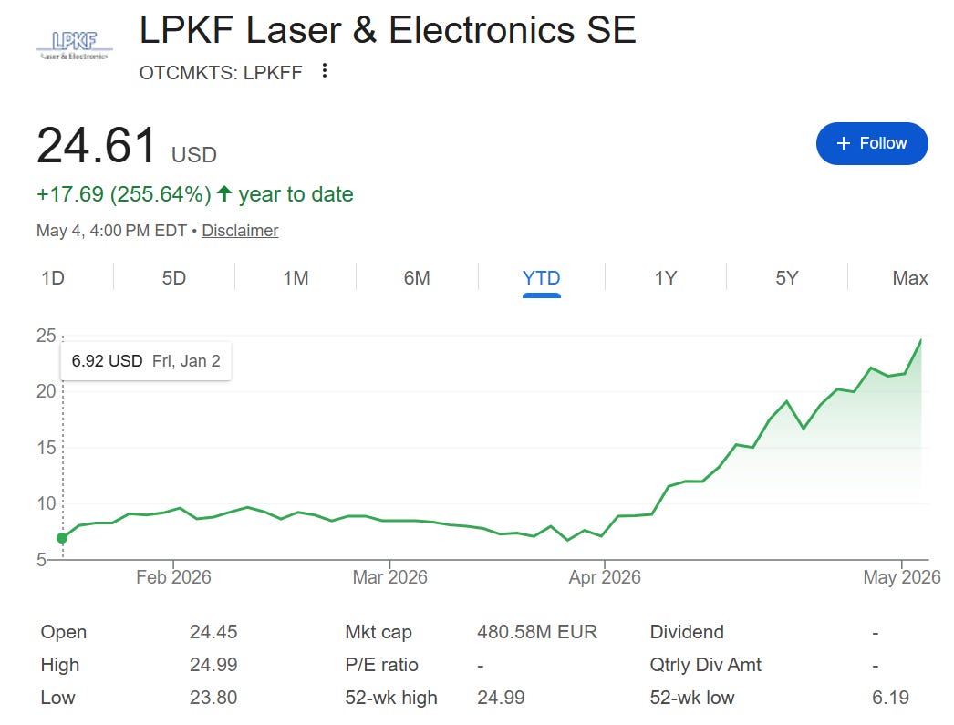
Over the same period, SMH (VanEck Semiconductor ETF) is up +42%, Applied Materials +46%, and ASML +19%. This has been a strong year for semiconductor equipment stocks. And yet a €115M-revenue German mid-cap is delivering multiples of the sector’s best names. Why?
The answer is not LPKF’s brand. It is one process LPKF controls: LIDE (Laser-Induced Deep Etching). This is the most advanced production-grade process for drilling Through Glass Vias (TGVs) in glass substrates. Other approaches exist, including CO₂ laser and laser modification plus etch. But LIDE is the most advanced commercial equipment platform capable of forming crack-free, debris-free vias at production speed, and LPKF is expanding it across the NEXAR LIDE 5000, Ablate 5000, and Bond 5000 product lines. As AI chip packaging begins shifting from organic substrates to glass, this process is becoming one of the key bottlenecks.
The thesis of this article is straightforward. Glass substrates are already needed in EIC (electronic packaging), and as the transition moves to CPO (co-packaged optics) and EPIC (electronic-photonic IC), glass’s structural advantage only grows. This article maps the equipment, material, and substrate companies sitting at the narrowest chokepoints of that transition.
So where is the most advantaged position in this transition?
To answer that, we first need to understand why glass is becoming necessary.
2. Technical Context: Why Glass Is Needed (EIC, CPO, EPIC)
2.1 Starting With EIC: Why Organic and Silicon Interposers Hit Their Limits
AI accelerator die sizes are growing. NVIDIA’s Blackwell B200 exceeded the reticle limit (~858mm²) by placing two dies in a single package, and the next generation Rubin is likely to carry even more chiplets. More dies require a larger interposer or intermediate substrate, and that is where existing materials begin to break down.
The organic substrate problem: CTE (coefficient of thermal expansion) is about 17 ppm/°C. In plain terms, for every 1°C temperature increase, the material expands by 17 millionths of its length. That sounds small, but across a 100mm package, these differences add up to microns. Silicon dies are about 2.6 ppm/°C. Bond the two together, and they expand and contract at different rates with every temperature change. At small sizes, this is manageable. At 110x110mm package sizes, warpage can reach hundreds of microns. Stack HBM 8 to 12 layers high next to an ASIC, and the substrate bows enough to crack bump joints.
The silicon interposer problem: CTE matches the silicon die, which is great. But it is expensive. Cutting interposers from 300mm wafers means high cost per area, and scaling to larger sizes is limited. The TSV (Through Silicon Via) process itself is not cheap either.
Glass solves both problems at once.
CTE: tunable from 3 to 5 ppm/°C. Composition can be adjusted to sit between silicon (2.6) and organic (17). [3]
Dielectric properties: Dk ~5, Df <0.005. Lower high-frequency signal loss than organic substrates.
Flatness: Glass surface roughness is in the single-nm range, more than an order of magnitude better than organic.
Panel-level processing: Glass can be processed on panels of 510x515mm and larger, covering 3 to 4 times the area of a 300mm wafer. That means more packages can be processed in each panel-level run.
This is why Intel officially announced glass substrates in 2023. Intel’s target is 10x interconnect density over organic, with production planned “before 2030” on its official roadmap. [4]
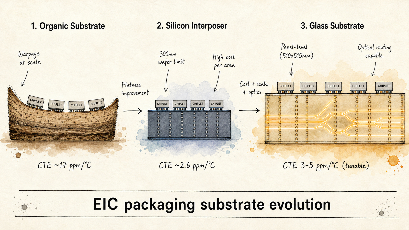
[Figure 1: EIC packaging substrate evolution: organic → silicon interposer → glass]
Key point: Glass is already recognized as a better substrate at the EIC stage because it addresses organic’s warpage and silicon interposer’s cost simultaneously. But glass’s real differentiation does not stop here.
2.2 When Light Enters the Picture, the Problem Changes: The Fiber-to-Chip Bottleneck in CPO
In EIC, only electrical signals need to pass through the substrate. In CPO (Co-Packaged Optics), optical fibers must be connected directly to photonic chips on the package substrate. That introduces an entirely different class of problem.
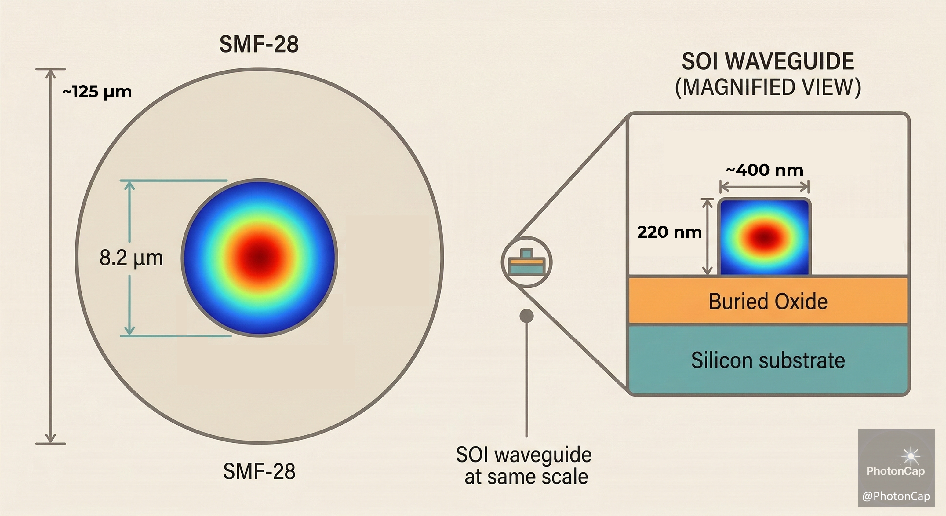
As discussed in PhotonCap PC101 Lecture 4, the hardest part of CPO packaging is the “last millimeter,” the fiber-to-chip coupling. [5] The core of this problem is not thermal expansion. It is mode field diameter (mode size) mismatch.
[PC101] Lecture 4:The Last Millimeter: Fiber-to-Chip Coupling and the CPO Packaging Bottleneck (Part 1)
![[PC101] Lecture 4:The Last Millimeter: Fiber-to-Chip Coupling and the CPO Packaging Bottleneck (Part 1)](https://substackcdn.com/image/fetch/$s_!qZxp!,w_1300,h_650,c_fill,f_webp,q_auto:good,fl_progressive:steep,g_auto/https%3A%2F%2Fsubstack-post-media.s3.amazonaws.com%2Fpublic%2Fimages%2Fa743aebb-02e3-496d-95cf-0da2962050b1_3590x2099.png)
Welcome back. This is PhotonCap.
A single-mode optical fiber (SMF-28) has a mode field diameter of about 8 to 10 µm at 1310nm. A silicon photonic chip waveguide, by contrast, has a cross-section roughly 0.5 µm wide and 0.2 µm tall. In mode area terms, that is about a 200x difference. Light coming out of the fiber is spread wide. The SiPh waveguide confines light in a tiny space. If the two are butt-coupled directly, coupling loss can reach tens of dB. The signal effectively vanishes.
This is why fiber-to-chip coupling always requires a mode size converter (spot size converter). The standard approach is to build edge couplers or grating couplers on the SiPh chip to expand the mode. But this alone has limits. Edge couplers can stretch the mode to ~3 to 4 µm, which still leaves a large gap against the fiber’s ~9 µm, and alignment tolerance stays within ±1 µm.
This is where glass enters. Ion-exchange (IOX) waveguides formed inside the glass substrate can be designed with a mode field diameter nearly matching the fiber, around 8 to 10 µm. That is why Corning’s IOX waveguide achieved <0.65 dB coupling loss against SMF-28 fiber. [6][20] The glass waveguide acts as an intermediate mode converter between fiber and PIC. The light path runs: fiber (~9 µm mode) into glass waveguide (~9 µm mode), then adiabatic taper down, then into PIC edge coupler (~3 to 4 µm mode). The mode shrinks in stages. Coupling is horizontal, through edge coupling.
Think of it this way: merging directly from an 8-lane highway (fiber) into a 1-lane alley (SiPh waveguide) creates a massive bottleneck. But routing through a 4-lane on-ramp (glass waveguide) first makes the merge smooth. In other words, glass provides an optical transition layer rather than forcing the fiber mode to collapse directly into the SiPh waveguide.
CTE (coefficient of thermal expansion) matching deserves a closer look here. Although both optical fiber and glass substrates are “glass,” they are not the same glass. Optical fiber is silica-rich glass with an extremely low CTE of ~0.5 ppm/°C, while packaging glass substrates are engineered borosilicate or aluminosilicate-type glasses with CTE typically in the 3 to 5 ppm/°C range. On CTE alone, silicon interposer (~2.6 ppm/°C) is actually closer to fiber than glass substrate is.
So where does glass’s CPO advantage come from, if not CTE? The combination, and mode size. Silicon interposers can also carry photonic waveguides. That is the logic behind silicon photonics and SiN photonic interposers. But the native silicon waveguide mode is far smaller than the fiber mode, so fiber coupling still requires additional spot-size converters, edge couplers, or other mode-transition structures. Glass IOX waveguides are different because they can be designed with mode sizes of ~8 to 10 µm, directly matching fiber. Add panel-level processing (510x515mm) and TGV electrical routing on the same substrate, and the picture changes. In an NVIDIA Spectrum-X class CPO package with 36 or more optical engines per package [19], the combination of fiber-matched waveguide mode, panel scalability, and integrated E/O routing is where glass has the clearest architectural advantage over silicon interposer.
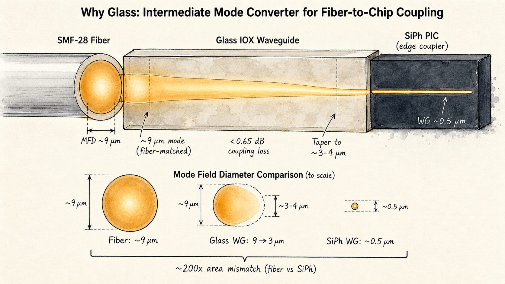
[Figure 2: Mode field diameter mismatch and glass waveguide as intermediate coupler]
Key point: The fundamental bottleneck in fiber-to-chip coupling is mode field diameter mismatch (fiber ~9 µm vs. SiPh ~0.5 µm). Silicon interposers can carry photonic waveguides, but native silicon waveguides still require mode-transition structures for efficient fiber coupling. Glass IOX waveguides provide a fiber-matched mode size while enabling panel scalability and integrated E/O routing on a single substrate.
2.3 At EPIC, Glass’s Structural Advantage Grows
At the EIC stage, glass was “a better foundation.” At the CPO stage, it was “a foundation that can safely attach fibers.” At EPIC (Electronic-Photonic Integrated Circuit), glass becomes not just a support structure but a routing platform that carries both electrical vias and optical waveguides.
Glass has a distinctive capability: ion-exchange can form optical waveguides directly inside the substrate body.
In alkali glass (containing Na), replacing sodium ions with silver (Ag) or potassium (K) ions raises the refractive index of the exchanged region. That refractive index contrast creates a waveguide that confines light. Corning’s IOX process has demonstrated propagation loss <0.1 dB/cm at 1310nm and chip coupling loss <0.65 dB. [6][20]
Why does this matter? Because a single glass substrate can do three things at once:
TGV (Through Glass Via) for vertical electrical signal routing
IOX waveguide for horizontal optical signal routing
Surface cavities for edge-coupling PICs (Photonic ICs) optically and flip-chip mounting ASICs electrically (bump bonding)
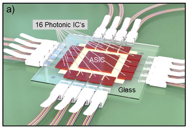
Corning’s OFC 2026 paper by Brusberg et al. demonstrated that the IOX-based GlassBridge platform can extend the glass substrate from a passive carrier to an active optical routing platform. [20] Based on PhotonCap’s analysis of the OFC 2026 presentation, the demonstrated structure placed 16 PICs and 1 ASIC on a 515x515mm glass panel, kept all electrical paths within 13mm, and achieved sub-5-minute placement time per PIC. [6]
![[OFC 2026] Part 3 of 5: Packaging: Glass Substrates to 3D Hybrid Bonding](https://substackcdn.com/image/fetch/$s_!tElU!,w_1300,h_650,c_fill,f_webp,q_auto:good,fl_progressive:steep,g_auto/https%3A%2F%2Fsubstack-post-media.s3.amazonaws.com%2Fpublic%2Fimages%2Ff9a73981-8047-4f7a-9f68-d64d56d2d650_2949x1557.png)
Alternative integration routes do exist. Polymer optical waveguides on organic substrates and SiN photonic waveguides on silicon interposers are both being explored. What differentiates glass is that the substrate itself becomes the optical routing layer while simultaneously supporting TGV-based electrical routing and large-area panel processing, all within a single platform. [21]
This is not a matter of material preference. It is a packaging architecture question. For a platform that routes electrical and optical signals at the substrate level while enabling panel-scale processing, glass is the most advanced candidate among publicly disclosed approaches.
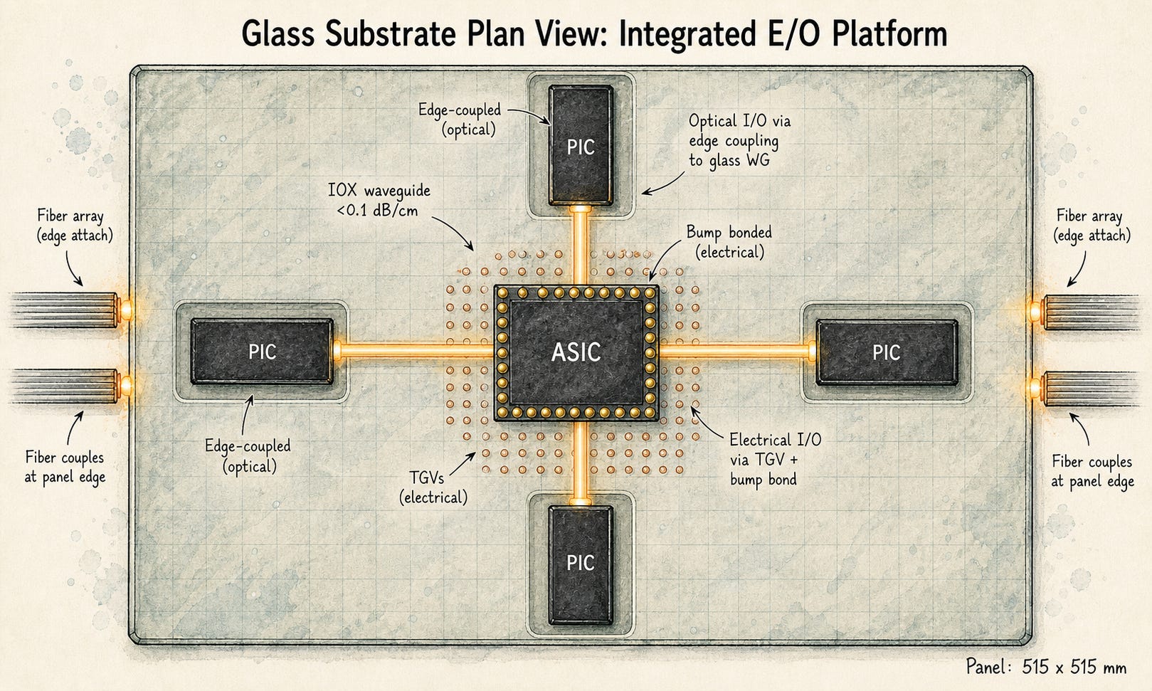
[Figure 3: Glass substrate plan view showing TGV + IOX waveguide + PIC edge coupling]
Key point: From EIC to CPO to EPIC, the structural advantage of glass compounds. At EIC, glass competes with organic and silicon. At EPIC, glass’s unique ability to integrate substrate-level optical routing becomes a clear differentiator against alternatives.
2.4 Why Now: The Timing Case
Glass substrate technology itself is not new. TGV processes appeared in academic papers by the mid-2010s. So why did it suddenly become an investment theme in 2025 and 2026?
Three things opened up on the demand side at the same time. First, NVIDIA Spectrum-X Photonics and Broadcom Bailly confirmed CPO on production roadmaps. Second, AI accelerator package sizes reached a point where organic substrate warpage becomes a real constraint. Third, glass core substrate pilot lines started spinning up simultaneously across Korea, the US, and Japan. [9]
Mass production timelines mostly target 2027, with some at 2028 to 2029. The current phase is pre-production equipment ordering and qualification. That is why the equipment companies are moving first.
Key point: Glass substrates are technically ready. Demand is pulling. Supply is following. Mass production targets are 2027 to 2029. What is moving right now is equipment and materials.
3. Three Layers of the Value Chain, One Complement, and Two Hidden Cards
Everything up to this point is visible from public sources alone.
The real differentiation starts here.
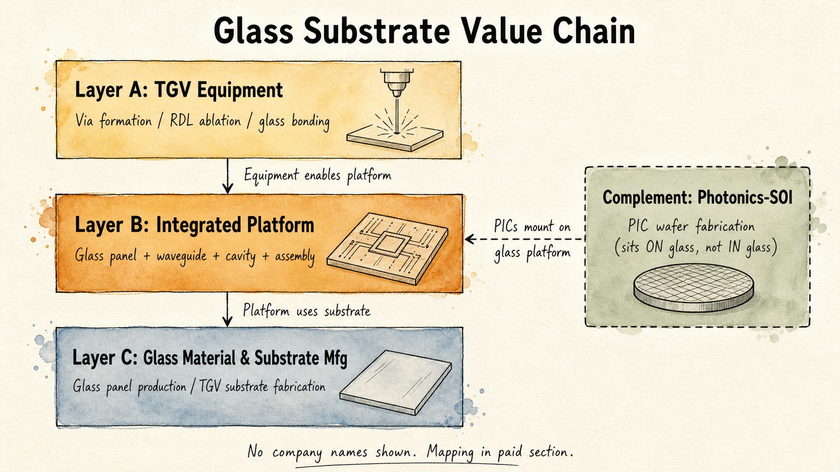
The glass substrate value chain breaks into three layers:
Layer A: The company with the most advanced TGV equipment position (equipment)
Layer B: The company embedding waveguides and building an integrated platform (integrated platform)
Layer C: Companies making the glass panels themselves (material / substrate fabrication)
Where is the most asymmetric position in this structure?
From public sources, glass substrates look like a long-term roadmap item for Intel, Samsung, and TSMC. But the real investment leverage is not in the material companies. It is in the equipment and routing platform players that control the pre-qualification bottleneck. Two hidden cards stand out.
Hidden Card 1: The Layer A (equipment) company’s patent coverage extends beyond TGV. Development of 3D waveguide formation inside glass is underway, meaning the equipment player could penetrate into integrated platform territory.
Hidden Card 2: The Layer B (integrated platform) company’s 16-PIC structure demonstrated at OFC 2026, if it reaches production, would put 4 to 8 times more PICs per panel than current CPO architectures. That changes assembly density entirely.
Layer A and Layer B offer very different risk/reward profiles within the same glass substrate theme.
[Figure 4: Glass substrate value chain, three layers, no company names mapped]
One More: A Company That Does Not Make Glass, but Grows With It
When glass packaging unlocks CPO yields, demand for PICs (Photonic ICs) increases. The starting wafer for those PICs is Photonics-SOI, and volume supply of that wafer is currently controlled by a single company. Glass substrates and Photonics-SOI are not horizontal competitors. They are vertical complements. (Detailed analysis: PhotonCap Soitec article [24])
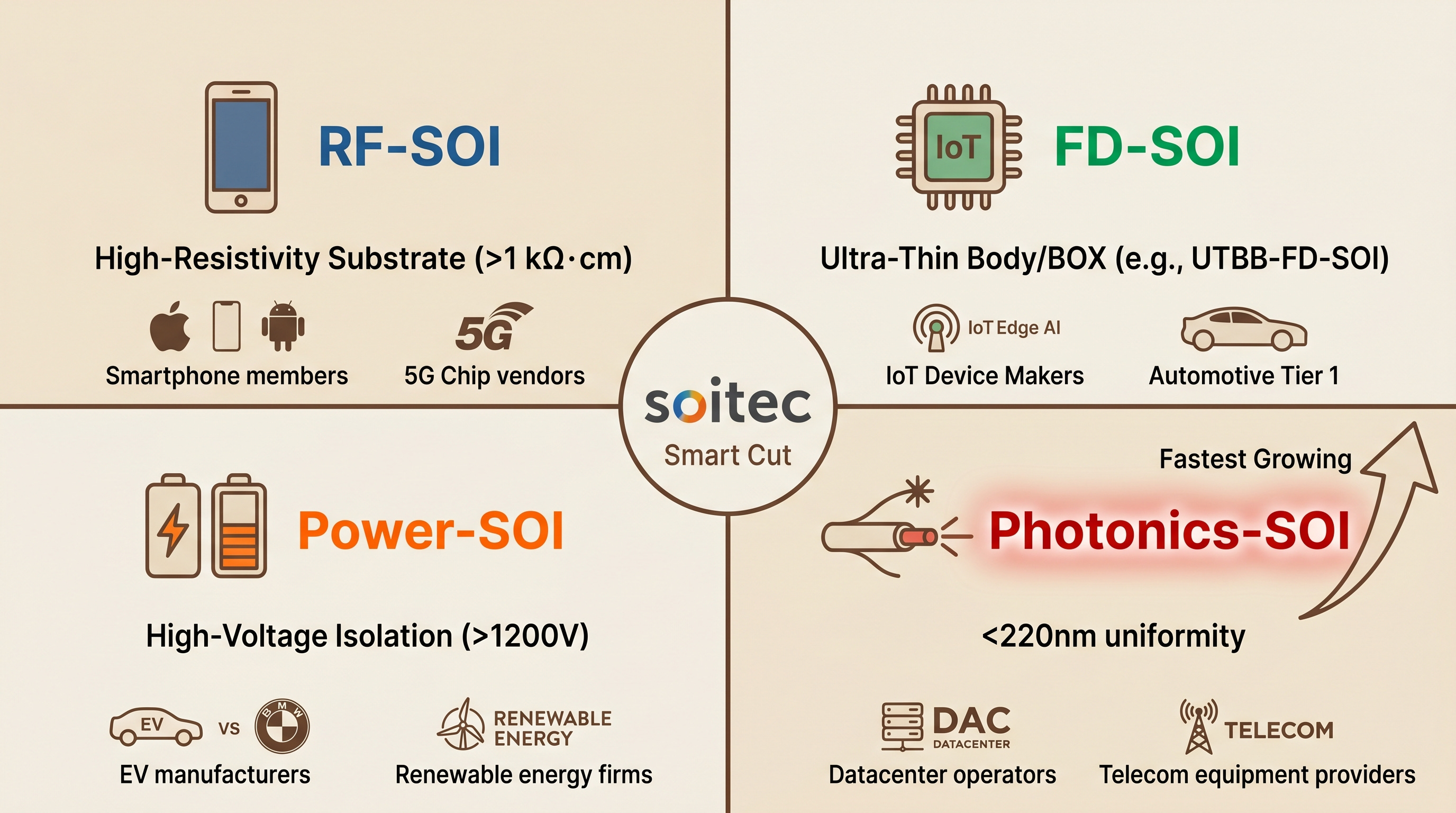
The Wafer That Used to Roll Around My Lab Is Now an AI Data Center Bottleneck: Soitec and the Investment Case for the Photonics-SOI Monopoly

As AI data centers accelerate the transition from electrical to optical interconnects, demand for SOI (Silicon-on-Insulator) wafers, the critical substrate for silicon photonics (SiPh), is growing rapidly. This article analyzes Soitec’s (EPA: SOI) technological moat (3,500+ Smart Cut patents, no competitor with meaningful Photonics-SOI volume identified from public sources), financial profile (FY2025 revenue of €891M, Photonics-SOI approaching €100M scale), and the reality behind the SiN platform threat narrative. Soitec’s stock rallied from its December 2025 low of €23 to €78 as of April 15, 2026, a YTD gain of +213%, as the market began pricing in its SiPh/CPO positioning. But the actual Photonics-SOI revenue scale-up is still in its early innings. The real test comes over the next 2 to 3 years as 1.6T/CPO ramps accelerate. Related tickers: $SOI (EPA), $SLOIF (OTC), $GFS, $TSEM
The paid section connects this complementary position to the glass substrate investment theme.
