
The 1% Loss Wall (Part 1): Where Xanadu ($XNDU) Really Stands, Through the Lens of Three Nature Papers

Xanadu Quantum Technologies (XNDU) is a Canadian company developing photonic quantum computers, listed on NASDAQ/TSX in March 2026 via SPAC merger. The deal was presented at approximately US$3.0B pre-money equity value and US$3.1B pro forma enterprise value, with roughly US$300M raised at close. In this article (Part 1), we analyze the three papers Xanadu published in Nature (Borealis 2022, Aurora 2025, GKP 2025) from a silicon photonics device perspective, tracing the progression from bulk optics to chip integration and the optical loss figures at each stage. All three papers converge on the same conclusion: “This technology works. But it is not yet fault-tolerant.” The gap comes down to one thing: optical loss in photonic devices. Part 2 covers the full component-level analysis and the PsiQuantum comparison table with investment implications.
Related tickers: XNDU, IONQ, RGTI, QBTS
Contents
Intro: Why Xanadu
Background: The IPO Story and Valuation
Borealis (2022): Quantum Advantage with a Programmable Photonic Processor
Aurora (2025): A Modular Photonic Quantum Computer Built from 35 Chips
GKP Qubits (2025): Generating Fault-Tolerant Qubits on an Integrated Photonic Chip
Closing + Part 2 Preview
References & Sources
1. Intro: Why Xanadu
In October 2019, Nature published an article titled “The quantum gold rush.”[1] It was a time when private capital was just starting to pour into quantum technology startups. By that point, 52 quantum companies worldwide had secured private funding. The article featured a man named Christian Weedbrook, running a quantum computing company called Xanadu in Toronto. He offered this comment on the quantum hype: “There is still a lot of value being created, it’s just a case of whether there is too much hype.”[1]
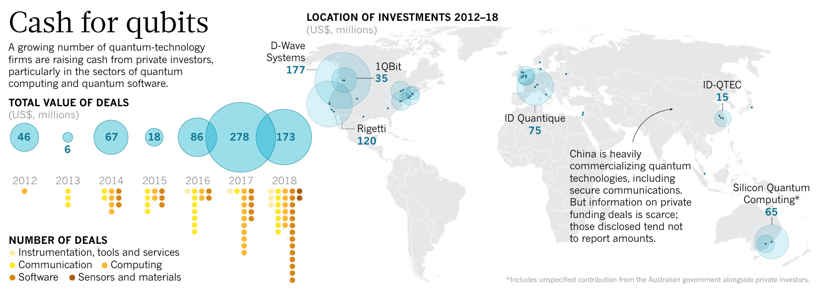
Figure 1: Nature 2019 “The quantum gold rush” article (doi:10.1038/d41586-019-02935-4) p.2, “Cash for qubits” infographic. Bubble chart showing quantum tech startup investment trends from 2012-2018. 52 companies, approximately $674M in cumulative deals.
Source: Nature (2019)
Six years later, in March 2026, Xanadu listed on NASDAQ and TSX simultaneously.[2] Ticker: XNDU. It became the world’s first pure-play photonic quantum computer company to go public. The deal closed via SPAC (Special Purpose Acquisition Company) merger with pre-money equity value of approximately US$3.0B and pro forma enterprise value of approximately US$3.1B, raising about US$300M.[3]
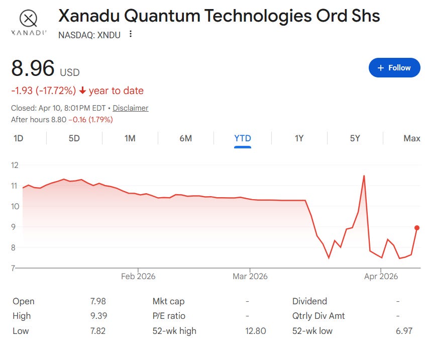
Here is one thing to note. Looking at how quantum computing companies have fared after going public, IonQ (IONQ), Rigetti (RGTI), and D-Wave (QBTS) all saw significant post-SPAC price volatility. Xanadu was no exception. SPAC deal reference price $10 → post-listing high $12.80 → low $6.97 → current $8.96 (as of April 10, 2026). Still -10.4% from listing price.[4] The listing structure includes Class A/B share distinctions, so market cap interpretations require some caution. Quantum computing stocks broadly rallied in late 2025 and corrected into 2026, but the recent single-day +17% bounce may signal that the market is starting to take another look.
There is one thing that sets Xanadu apart from other quantum companies. Three papers published in Nature, the flagship journal, in succession. Borealis in 2022, Aurora in 2025, GKP qubits in 2025. Quantum papers are plentiful, but publishing three hardware demonstration papers in Nature proper over three years is rare outside of Google Quantum AI.
The core idea of this article is straightforward. Read these three papers through the eyes of a Si-photonics engineer, and Xanadu’s current technical position and remaining challenges become very clear. We will touch on quantum mechanics along the way, but what ultimately matters for investment decisions is the loss performance of photonic devices.
2. Background: The IPO Story and Valuation
Company Overview
Xanadu Quantum Technologies was founded by Christian Weedbrook in Toronto in 2016. The goal is to build a quantum computer using photons. Unlike Google and IBM, which use superconducting qubits, or IonQ, which uses trapped ions, Xanadu takes a different approach. It uses light, specifically squeezed light at 1,550 nm, the same wavelength band used in telecom optical fiber.
Let me explain squeezed light first. Normal laser light has equal quantum uncertainty (noise) in both quadrature components of the electromagnetic field: amplitude (q) and phase (p). Squeezed light compresses the noise in one direction while expanding it in the other. Think of squeezing a balloon from one side: the other side bulges out. The total air (total noise) stays the same, but the shape changes. Due to the uncertainty principle, you cannot reduce total noise, but by encoding information on the “quiet side,” more precise quantum operations become possible. Xanadu generates this squeezed light using microring resonators on chip.
Before going public, the company raised a total of US$250M in private funding, and in 2023 received CAD$40M from Canada’s Strategic Innovation Fund.[5]
PennyLane: A Software Asset Separate from Hardware
If you view Xanadu purely as a “hardware company,” you are missing something. The company develops PennyLane, an open-source quantum programming library. Its key feature is that it is hardware-agnostic: it connects to nearly every quantum hardware backend including IonQ, Rigetti, Quantinuum, IBM, and Google, and integrates with ML frameworks like PyTorch and TensorFlow.
This is why Xanadu’s partner page features logos of competitors IonQ, Rigetti, and Quantinuum side by side. The company is positioning PennyLane as the PyTorch of the quantum software ecosystem. Other partners fall into four categories: foundries/semiconductors (GlobalFoundries, AMD, imec, Ligentec), cloud deployment channels (AWS, Google, IBM), quantum algorithm proof-of-concept customers (VW battery simulation, BMW quantum ML), and Canadian quantum research hubs (University of Toronto, NRC, IQC, Mila).
With no meaningful hardware revenue yet (2025 annual revenue was US$4.6M, mostly from SW/cloud), PennyLane’s paid services and cloud runtime sales are effectively Xanadu’s only revenue stream. Since PennyLane itself is open-source, the monetization path remains uncertain. Whether a Red Hat or Databricks-style enterprise services model is viable, or whether it merely helps slow the burn rate until hardware ships, is still an open question.
Why SPAC?
On November 3, 2025, Xanadu announced a merger with Crane Harbor Acquisition Corp., a SPAC.[3] CEO Weedbrook was candid about the background: the Series D fundraising was progressing slower than expected, and he viewed the SPAC route as a “well-worn path.”[6] IonQ, Rigetti, and D-Wave had all gone public via SPAC before.
Deal terms called for approximately US$225M from the Crane Harbor trust account plus US$275M in PIPE (Private Investment in Public Equity), targeting total gross proceeds of about US$500M.[7] The final close came in at approximately US$300M.[8] More than 90% of PIPE investment came from new investors rather than existing Xanadu shareholders.[8]
One cautionary note: when D-Wave went public via SPAC in 2022, 97% of trust account holders chose redemption, leaving just US$9M.[6] Weedbrook acknowledged this risk and mentioned that he tried to push out positive news before listing to reduce the redemption rate.[6]
Current Valuation
Pro forma enterprise value: approximately US$3.1B (SPAC deal basis)[7]
Current price: US$8.96 (as of April 10, 2026, +17.12% day-over-day)[4]
Current market cap: approximately US$2.8B on a pro forma basis (note: Class A/B share structure and fully diluted basis may affect interpretation)[4]
52-week range: US$6.97 - $12.80[4]
CEO stake: Weedbrook holds 46,432,704 Class A Multiple Voting Shares. 15.58% of total outstanding shares, 17.92% of voting power. 51.8% of Class B shares on an as-converted basis. 180-day lock-up applies (~September 2026).[16]
Revenue: US$4.6M for 2025, still early stage. Centered on PennyLane SW licenses + cloud runtime sales. No meaningful hardware revenue yet.
At $8.96 vs. the $10 listing price, it is still in the red. But it has bounced +28% from the $6.97 low. The +17% single-day move suggests short-term momentum, but the investment thesis at this point depends far more on the technology roadmap than on financials.
One governance point worth noting. On April 2, 2026, days after listing, an SEC Schedule 13D filing revealed that CEO Weedbrook holds 51.8% of Class B shares on an as-converted basis.[16] His actual outstanding share count is 15.58%, but the Class A Multiple Voting Share structure gives him controlling influence. Among quantum computing companies, it is rare for a founder to maintain this level of control through a public listing. The 180-day lock-up (expiring around September 2026) and what happens after is one variable to watch.
Project OPTIMISM
On March 11, 2026, Xanadu announced it had entered negotiations with the Canadian federal and Ontario provincial governments for up to CAD$390M (approximately US$280M) in quantum manufacturing infrastructure support.[9] The project, called OPTIMISM, aims to build domestic capabilities in:
Heterogeneous integration
Photonic integrated circuit (PIC) packaging
Wafer-level semiconductor test and measurement
Quantum module assembly
Final contract has not been signed. Due diligence and formal agreements remain.[9] The timing of this announcement, right before listing, was also strategic to reduce SPAC redemption rates.
Key takeaway: Xanadu is the world’s first pure-play photonic quantum computer company to go public via SPAC. The deal was structured at approximately US$3.1B pro forma EV. Current price is $8.96 (as of April 2026, -10% from listing price). 2025 revenue was US$4.6M, still early stage. Negotiations for CAD$390M in government manufacturing support are in progress.
Now let us look at what the technology can actually do, through the lens of three Nature papers.
3. Borealis (2022): Quantum Advantage with a Programmable Photonic Processor
In June 2022, Xanadu published its Borealis photonic processor in Nature.[10] The core claim: a photonic machine with dynamic programmability over all quantum gates demonstrated quantum computational advantage on a specific task called Gaussian Boson Sampling (GBS).
An important distinction here. Quantum computational advantage means “solving a problem faster than the best supercomputers running the best known algorithms.” But this is not general-purpose quantum computing. GBS is a task of sampling from a specific probability distribution, and it does not directly solve practical problems. An analogy: rather than acing the entire math exam, the machine solved one particular type of problem faster than any existing calculator. Google made a similar claim in 2019 using superconducting qubits (random circuit sampling), and Xanadu did it with photons.
China’s USTC had previously claimed photonic quantum advantage with Jiuzhang, but that machine had a fixed interferometer. It was a static, non-programmable structure, and was criticized for being vulnerable to classical spoofing.[10] Borealis aimed to solve both issues.
System Architecture
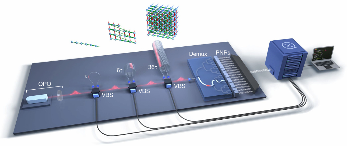
Figure 2: Borealis paper (Nature 2022, doi:10.1038/s41586-022-04725-x) p.2 Fig.1. Full optical circuit from OPO source → 3-stage fiber loops (τ, 6τ, 36τ) → VBS → 1-to-16 demux → 16-channel TES detectors.
Source: "Madsen et al., Nature (2022)"
From a Si-photonics engineer’s perspective, this system is not a chip-integrated system. It is based on bulk optics and fiber.
Let me clarify the difference between “bulk optics” and “chip integration.” This distinction is central to understanding Xanadu’s technology evolution.
Bulk optics means placing individual optical components, like lenses, mirrors, and crystals, one by one on an optical table and aligning them. Think of the complex equipment setups you see in university physics labs. Each component is fingertip to fist-sized, and the spacing between components is centimeters to meters. Precision is possible, but scaling up means filling an entire room and beyond.
Chip integration (photonic integrated circuit, PIC) puts all these optical components onto a semiconductor chip. Just as smartphones pack billions of transistors, optical components can be integrated at micrometer scale on chip. Component spacing shrinks to sub-millimeter, and hundreds to thousands of identical chips can be produced from a single wafer.
Why does this matter? A practical quantum computer requires millions of optical components.[11] Bulk optics cannot physically scale to that level. Mass production like semiconductors is required, and that means going to chips. Xanadu’s three papers over three years show exactly this journey: Borealis (bulk, 2022) → Aurora (35 chips, 2025) → GKP (custom chip, 2025). And the biggest challenge in moving from bulk to chip is optical loss. In bulk optics, light travels through air. On chip, it travels through narrow waveguides, bouncing against walls and leaking out.
Now let us walk through Fig.1 from left to right.
OPO (light source): 1,550 nm OPO (Optical Parametric Oscillator). KTP crystal pumped at 775 nm to generate squeezed light. 6 MHz repetition rate, producing 6 million pulses per second. Bulk cavity.
Three fiber loops (τ, 6τ, 36τ): This is the heart of Borealis. When a pulse travels through a loop, it gets delayed. An earlier pulse and a later pulse meet at the VBS, creating quantum interference.
τ loop: connects pulse N with N-1 (immediate neighbor) → 1D chain
6τ loop: connects pulse N with N-6 → 2D sheet
36τ loop: connects pulse N with N-36 → 3D cube
Take 216 pulses arriving in sequence and fold them in groups of 6: the result is a 3D lattice. Physically it is a single fiber, but the connectivity structure is three-dimensional. Why 1, 6, and 36? They are powers of 6 (6⁰, 6¹, 6²), which is what makes the folding work cleanly. 6×6×6 = 216 modes in a cubic lattice.
[1D] τ only: 1-2-3-4-5-6-7-8-...     (neighbor connections)

[2D] τ + 6τ:
 1 - 2 - 3 - 4 - 5 - 6            (horizontal: τ)
 |   |   |   |   |   |            (vertical: 6τ)
 7 - 8 - 9 -10 -11 -12

[3D] τ + 6τ + 36τ: stack 6 sheets, connect layers via 36τ
VBS (Variable Beam Splitter): The key component between each loop. It controls “what fraction of this pulse goes into the loop vs. straight through,” adjustable by voltage. Uses electro-optic modulators (EOM, QUBIG GmbH), and the ratio can change with every pulse. This is what makes it “programmable.” Each run specifies 1,296 real parameters, all of which are VBS settings. Jiuzhang lacks this tunability, which is why its squeezer gain (G) is fixed.
Demultiplexer (Demux): 1-to-16 binary switch tree. The OPO fires at 6 MHz, but each TES can only handle 375 kHz. TES detectors work by briefly leaving the superconducting state when a photon arrives, and the recovery time is too long for high-rate pulses. So the demux distributes pulses round-robin to 16 TES units: 6 MHz ÷ 16 = 375 kHz per detector. Restaurant analogy: 600 orders per minute coming in, one chef handles 37. Solution: 16 chefs taking turns.
TES detectors (PNRs): 16 TES (Transition Edge Sensor) based PNR (Photon Number Resolving) detectors inside a cryogenic refrigerator. 95% detection efficiency. Each detector counts “how many photons arrived” for each pulse. The measurement result across 216 pulses is an integer vector of 216 numbers, for example (3, 0, 7, 2, 5, ..., 4). Not binary. This vector is one sample.
What GBS Actually Does
One important clarification here. Borealis does not produce 0101-style binary computation.
Squeezed light passes through the interferometer (loops + VBS), and the TES detectors count photons. The result is an integer vector like (3, 0, 7, 2, ...). These vectors appear random but actually follow a specific probability distribution determined by the VBS settings. Some combinations appear frequently, others almost never.
For a classical computer to draw a “genuine” sample from this distribution, it must compute a mathematical function called the Hafnian, whose computational cost explodes exponentially with the number of modes. At 216 modes, a supercomputer would need 10⁹ years.
Borealis does not compute. It fires light and counts. Physics automatically produces a sample from that distribution in 36μs. Physics itself acts as the computer. The catch is that this “sampling” task has no practical application today. Think of a Nurburgring lap time record: the record itself is not useful for daily driving, but it proves that the engine (squeezed light) and chassis (programmable interferometer) perform under extreme conditions.
Performance Numbers
Maximum detected photon count: 219
Mean photon number: 125
Time per sample: 36 μs (Borealis) vs. 9,000 years (Fugaku supercomputer, exact method)[10]
Runtime gap vs. previous photonic quantum advantage experiments: 50 million times larger
Cross-entropy benchmark: experimental data outperformed all 5 classical spoofers (squashed, thermal, coherent, distinguishable squeezed, greedy)
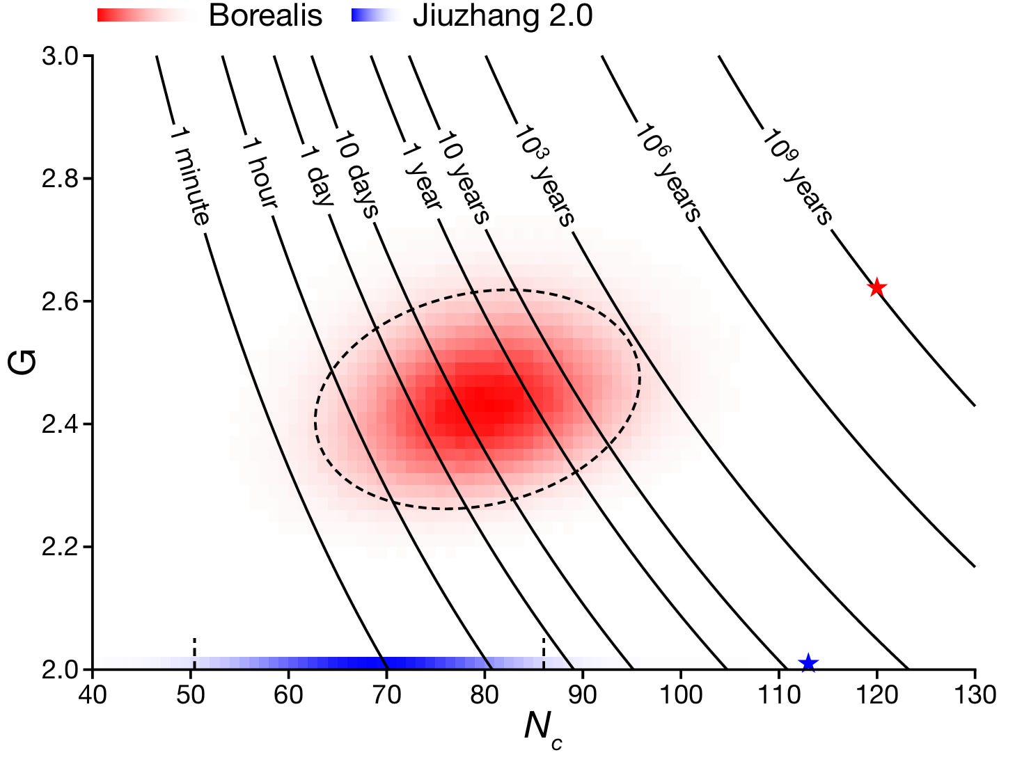
Figure 3: Borealis paper p.5 Fig.4c. X-axis: Nc (number of clicks, detected photon count), Y-axis: G (mean gain of squeezers). Diagonal contour lines show classical simulation time for each (Nc, G) combination (1 minute to 10⁹ years). Red distribution: Borealis experimental data (G is programmable), red star: Borealis maximum quantum advantage point (Nc≈112, G≈2.58). Blue distribution: Jiuzhang 2.0 (G≈2.0 fixed, not programmable), blue star: Jiuzhang maximum point (Nc≈113, G=2.0). Borealis can move along both axes, cutting diagonally across contour lines, making classical simulation millions of times harder at the same Nc.
Source: “Madsen et al., Nature (2022), Fig.4c”
Here is how to read this graph.
Axes: X-axis Nc is the number of photons detected by TES. Due to quantum mechanics, this varies with every run even under identical settings. Y-axis G is the squeezer gain, a value the experimenter sets via VBS.
Diagonal contour lines: Like contour lines on a hiking map that connect points of equal elevation, these connect points where classical simulation takes the same amount of time: 1 minute, 1 hour, 10 days, 1 year, 10³ years, 10⁶ years, 10⁹ years. Moving toward the upper right, the time increases exponentially. The contour lines are just a “map.” They contain no information about any specific machine.
Red region (Borealis): A heatmap of millions of experimental runs. Darker red means that (Nc, G) combination appeared more frequently. G was varied across multiple settings, and Nc spread probabilistically at each G. The red star (★) marks the most extreme point reached (Nc≈112, G≈2.58), landing on the 10⁹-year contour.
Blue region (Jiuzhang 2.0): Distributed only along the G=2.0 horizontal line. The interferometer is fixed, so G cannot be changed. It moves only in the Nc direction. The blue star (★) is Jiuzhang’s maximum (Nc≈113, G=2.0), ending near the 10³-year contour.
Dashed circles: Statistical confidence intervals (1σ, 2σ). “68%/95% of results fall within this boundary.”
Key comparison: Borealis and Jiuzhang have similar Nc (~112-113), but Borealis can increase G, cutting diagonally across the contour lines. At the same photon count, simulation difficulty jumps from 10³ years to 10⁹ years, a million-fold increase. On the Borealis side, sampling time is always 36μs regardless of G or Nc. The times shown on the contour lines are entirely “the classical computer’s side.” The value of “programmable” is captured in this single graph.
Significance and Limitations from a Si-Photonics Perspective
The key point: Borealis is not a chip-integrated system. The OPO is bulk KTP crystal. The interferometer is fiber loops. The EOM is an external module. The only “semiconductor-adjacent” part is the NIST-made TES detectors.
Still, several device-level numbers from this experiment are notable:
Net transmittance: approximately 33% (≈4.8 dB loss). Two-thirds of photons are lost through the interferometer path.[10] Imagine a plumbing system where you put in 100 liters and only 33 arrive at the other end. In a quantum computer, this “leaking water” is information loss, and reducing it is the central challenge of this entire article.
TES detection efficiency: 95%[10]
Squeezing parameter: mean r ≈ 1.1 (approximately 9.6 dB squeezing)[10]
Schmidt number K: 1.12 (g⁽²⁾ = 1.89). Ideal is K=1. At 1.12, the source is nearly single-mode.[10]
Phase noise: first loop 0.02 rad, second 0.03 rad, third 0.15 rad[10]
What Borealis demonstrated is a proof of concept: quantum advantage is possible with photons. But this is a bulk optical system that is difficult to scale, and it is far from fault tolerance. Fault tolerance means the ability to detect and correct errors in real time so the system operates correctly even when individual components fail. Think of it like redundant safety systems in an aircraft. If one engine fails, the plane keeps flying on the remaining engines. Similarly, if one qubit produces an error, the overall computation still proceeds correctly. This is the ultimate goal for every quantum computer. The next step was to move this onto chips.
Key takeaway: Borealis demonstrated quantum advantage with 216 modes, up to 219 photons, and a 9,000-year vs. 36μs gap against Fugaku. But it was a bulk optical system with only 33% net transmittance. Chip integration and loss reduction were the next challenges.
After Borealis proved the principle, Xanadu moved the system onto chips within three years. That machine is Aurora.
4. Aurora (2025): A Modular Photonic Quantum Computer Built from 35 Chips
Published online in January 2025 and in the February 2025 issue of Nature, the Aurora paper is Xanadu’s second Nature publication.[11] The subtitle says it all: “Scaling and networking a modular photonic quantum computer.”
Where Borealis demonstrated quantum advantage with bulk optics, Aurora is a modular system built from 35 photonic integrated circuit (PIC) chips connected by optical fiber. It fits in four server racks.
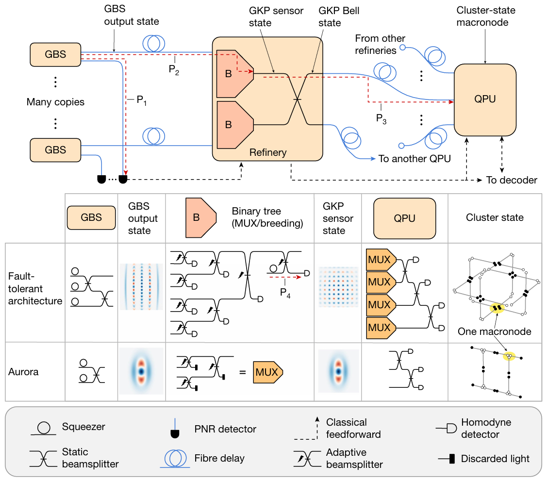
Figure 4: Aurora paper (Nature 2025, doi:10.1038/s41586-024-08406-9) p.3 Fig.1. Full 3-stage architecture: Stage 1 GBS Source (24 SiN chips) → Stage 2 Refinery (6 TFLN chips) → Stage 3 QPU (5 Si photonics chips). Fiber delay lines between stages.
Source: “Aghaee Rad et al., Nature (2025)”
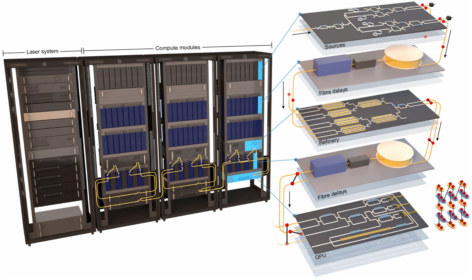
Figure 5: Aurora paper p.13 Extended Data Fig.1. Photo of Aurora system deployed in 4 server racks.
Source: “Aghaee Rad et al., Nature (2025)”
System Configuration
Aurora has a 3-stage architecture:
Stage 1: GBS Source
24 SiN (silicon nitride) chips (21 active + 3 spares)
4 squeezers per chip, 84 total
42 GBS cells generating 36 heralded non-Gaussian states
36 PNR (TES) detectors for heralding
Stage 2: Refinery
6 TFLN (Thin-Film Lithium Niobate) chips
Two 4-to-1 binary switch trees per chip (12 total)
Multiplexing selects optimal input pairs
Output: 6 entangled Bell pairs
Stage 3: QPU (Quantum Processing Unit)
5 Si photonics chips (AIM Photonics 300mm platform)
SiN waveguide inputs, transition to Si waveguides, Ge photodiode homodyne detection
12-mode homodyne measurement every clock cycle
FPGA-based real-time decoder
Phase- and polarization-stabilized fiber delay lines connect the stages.
Key Experimental Results
Cluster state generation: 12 spatial modes x 7.2 billion temporal modes = 86.4 billion modes of cluster state, continuously generated and measured over 2 hours.[11] A cluster state is like a “canvas” for quantum computing. Many qubits are entangled in a lattice structure, and computation proceeds by measuring them one by one. A larger, more uniform canvas enables more complex computations.
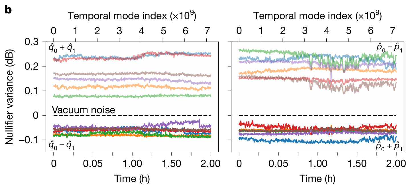
Figure 6: Aurora paper p.5 Fig.3b. X-axis: time (0-2 hours), Y-axis: nullifier variance (dB relative to vacuum noise). Time-series data showing all 12 spatial modes staying below vacuum level for the full 2 hours.
Source: “Aghaee Rad et al., Nature (2025)”
The nullifier variance stayed below vacuum noise level for the entire 2 hours. This means squeezing was maintained, and entanglement between chips persisted without interruption. Even with approximately 14 dB of optical loss across the full path.
Real-time decoding + feedforward: A distance-2 repetition code was implemented, with the FPGA decoder changing the measurement basis of the next clock cycle in real time based on previous measurement results.[11] Total signal chain latency was approximately 976 ns: 240 ns for homodyne → ADC → normalization, 672 ns for serial link latency, and 64 ns for the decoder algorithm.[11]
Three-Platform Chip Architecture
From a Si-photonics perspective, this is the most interesting part. Aurora uses three different PIC platforms simultaneously:
Role Platform Foundry Wafer Size Chip Size Source SiN Ligentec / X-Fab 200mm 8 × 5 mm Refinery TFLN HyperLight - 14.6 × 4.5 mm QPU Si photonics (SiN+Si+Ge) AIM Photonics 300mm 6.2 × 4.3 mm
Each stage demands different optical characteristics, so no single platform can be optimal. Like building a car with engine (power), transmission (control), and dashboard (measurement) each made from different materials and processes.
Source needs nonlinearity. Uses SiN’s third-order nonlinear effect (SFWM, Spontaneous Four-Wave Mixing).
Refinery needs high-speed electro-optic switching. TFLN is well suited for this.
QPU needs integrated photodiodes. Si photonics Ge PDs fill this role.
Personally, I think this three-platform architecture is Xanadu’s most distinctive feature. The tradeoff is that heterogeneous chip-fiber-chip interconnects pile up, and loss accumulates at every junction.
Fault Tolerance Threshold: The Loss Gap
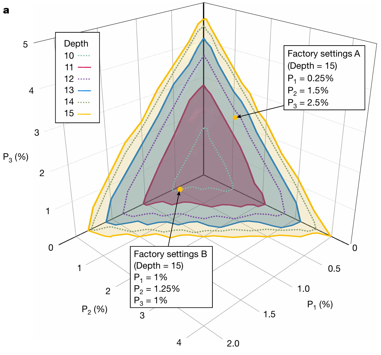
Figure 7: Aurora paper p.6 Fig.4a. 3D surface plot. X-axis: P1 loss(%), Y-axis: P2 loss(%), Z-axis: P3 loss(%). Overlapping surfaces colored by depth (10-15). Inside surface = fault tolerance possible. Factory Settings A (P1=0.25%, P2=1.5%, P3=2.5%) and B (P1=1%, P2=1.25%, P3=1%) marked as yellow target points.
Source: “Aghaee Rad et al., Nature (2025)”
This is the most important figure in the Aurora paper for investment purposes. Here is how to read it.
Three axes: P1, P2, P3 are the loss (%) of Aurora’s three optical paths. All three paths must simultaneously have low loss for fault tolerance. One good path is not enough.
Colored surfaces: Each color represents the fault tolerance boundary for a different depth (quantum circuit depth). Inside the surface = pass, outside = fail. Deeper depth means more complex computations are possible, but the loss tolerance gets tighter. The yellow surface (depth 15) is the largest. The red surface (depth 11) is smaller. Deeper depth, smaller allowed region.
Two Factory Settings points: Target operating points proposed by the paper.
A (P1=0.25%, P2=1.5%, P3=2.5%): extremely low P1, more headroom on P3
B (P1=1%, P2=1.25%, P3=1%): all three paths uniformly low
Both sit inside the depth-15 surface, meaning fault tolerance is achievable at those loss levels. These are “get loss down to here and it works” targets.
Where is Aurora today? Look at the axis ranges: P1 goes from 0 to 2%, P2 from 0 to 4%, P3 from 0 to 5%. Aurora’s current operating point is P1=56%, P2>95%. It does not even appear on the graph. It is far outside the axis range. Reducing P1 from 56% to Factory Settings B’s 1% requires a 56x improvement. To Factory Settings A’s 0.25%, it is 224x. This is what the paper authors mean when they say “20-30x improvement on a dB scale.”
Bottom line: light is leaking massively on its way from one chip to the next. Think of it as shipping packages. You send 100 from the origin, but only 44 arrive. For the quantum computer to work properly, 99 need to arrive:
P1 (squeezer → PNR): currently ~56% loss. 100 photons in, 44 arrive. Target: 99 arriving.
P2 (squeezer → refinery homodyne): P1+P2 combined currently >95% loss. Less than 5 out of 100 remain.
P3 (refinery output → QPU homodyne): target ~1-2.5% or less.
The Aurora paper authors are candid about this gap. On a dB scale, component insertion loss needs to improve by a factor of 20-30x for fault-tolerant operation.[11]
This is a very honest statement. “Our system works. We integrated all functional blocks. But performance is still far from threshold.” That is the tone. The fact that the current operating point does not even fit on the graph’s axis range tells you, more clearly than any number, where this company is today and how far it needs to go.
Key takeaway: Aurora is a scale model of a modular quantum computer connecting SiN, TFLN, and Si photonics chips over fiber. It demonstrated 86.4 billion-mode cluster state generation and real-time decoding. But the current operating point (P1=56%) does not even appear within the fault tolerance threshold graph’s axis range (P1: 0-2%). The gap is 20-30x on a dB scale.
If Aurora showed system-level feasibility, the next question is “Can you actually make fault-tolerant qubits on a photonic chip?” The third Nature paper, from June 2025, addresses that question.
5. GKP Qubits (2025): Generating Fault-Tolerant Qubits on an Integrated Photonic Chip
In June 2025, Xanadu published its third Nature paper.[12] Title: “Integrated photonic source of Gottesman-Kitaev-Preskill qubits.” Let me explain what GKP qubits are.
Why GKP Qubits Matter
GKP stands for Daniel Gottesman, Alexei Kitaev, and John Preskill, three theoretical physicists. This encoding scheme was proposed in 2001.
Here is an analogy. A conventional qubit stores information as “photon present / not present” (0 or 1). A GKP qubit stores information by stamping a comb-like pattern into the light wave itself. Regularly spaced peaks in phase space distinguish 0 from 1. If you think of it in musical terms, a conventional qubit is “note present / absent,” while a GKP qubit encodes information in a “harmonic pattern repeating at specific frequency intervals.” If the comb spacing is narrow and uniform enough, the original information can be recovered even when some noise creeps in. That is why it is called a “fault-tolerant” qubit.
There are multiple ways to encode qubits in quantum computers. GKP encoding stores qubit information in the electromagnetic field quadratures. The key advantage: gate operations can be implemented deterministically using only beamsplitters, phase shifters, and homodyne detectors.[12] No probabilistic gates like superconducting qubits require, and most operations can run at room temperature.
The catch is that GKP qubits are hard to create. Squeezed light must be heralded through nonlinear interference and photon-number detection. Here is how that works.
The GKP chip has 3 TES detectors attached for heralding. After squeezed light passes through the interferometer, these 3 TES each count how many photons arrived, and based on those counts, the system judges whether “the state produced this time is usable as a GKP qubit.” The counts from each TES are written as (n₁, n₂, n₃). For example, (3, 3, 3) means “TES 1 detected 3, TES 2 detected 3, TES 3 detected 3.”
Not all patterns are usable. If an unsuitable pattern like (2, 1, 4) comes up, that result is discarded. Out of 12.8 billion repetitions, only the cases where (3, 3, 3) appeared were selected for analysis. Success rate: 0.029%, about 30 Hz. The vast majority fail. Only a tiny fraction “pass.”
Experimental Setup
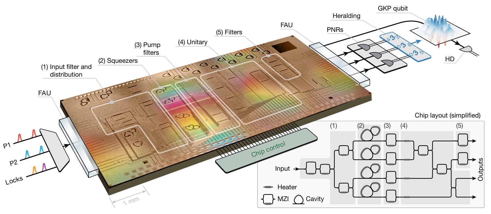
Figure 8: GKP paper (Nature 2025, doi:10.1038/s41586-025-09044-5) p.2 Fig.2. Top: 300mm SiN chip layout (4 squeezers, MZI filters, staircase interferometer). Bottom: off-chip setup (3 TES heralding + 1 balanced homodyne).
Source: “Larsen et al., Nature (2025)”
The chip was fabricated on a custom 300mm SiN wafer platform. Compared to Aurora’s source chips on Ligentec’s 200mm commercial line, the GKP chip uses a custom process optimized for low loss.[12]
On chip:
4 squeezers (photonic molecule microrings)
Asymmetric MZI filters (pump removal)
Programmable interferometer (staircase structure)
Off chip:
3 TES PNR detectors (for heralding)
1 balanced homodyne detector (for state tomography)
Operating at 200 kHz repetition rate, a total of 12.8 billion repetitions of data were collected.[12]
GKP State Measurement Results
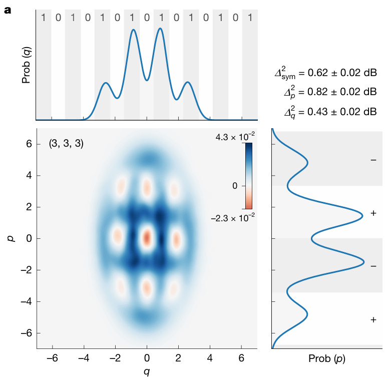
Figure 9: GKP paper p.3 Fig.3a. Wigner function 2D density plot of the state heralded by (3,3,3) PNR pattern. 3x3 grid of alternating negative (blue) and positive (red) regions.
Source: “Larsen et al., Nature (2025)”
The Wigner function of the state heralded by the (3, 3, 3) PNR pattern shows a clear 3 × 3 grid structure of negative regions in phase space.[12] This is the hallmark of a non-Gaussian state. Both q and p quadratures show at least 4 resolvable peaks, a structural requirement for fault tolerance.
Quantitative numbers:
Symmetric effective squeezing: 0.62 ± 0.02 dB[12]
p-effective squeezing: 0.82 ± 0.02 dB
q-effective squeezing: 0.43 ± 0.02 dB
Stabilizer expectation values: |⟨Ŝ_p⟩| = 0.273, |⟨Ŝ_q⟩| = 0.241
Success probability: 2.9 × 10⁻⁴ (≈30 Hz success rate)[12]
Here is the critical comparison. The Aurora paper established a fault tolerance threshold of 9.75 dB.[11] The GKP paper achieved symmetric effective squeezing of 0.62 dB. The gap is approximately 9.1 dB.
Symmetric effective squeezing is a quality score for the GKP qubit. Higher is better. 9.75 dB is the passing line: “score above this and fault tolerance is possible.” 0.62 dB is the current score. On an exam analogy, the passing grade is 97.5 out of 100, and the current score is 6.2. The reason it is so low is loss. When photons disappear en route, the GKP qubit’s comb pattern blurs, and the ability to distinguish 0 from 1 degrades. That degradation shows up as a lower squeezing score.
You might wonder: “If some photons are lost, can’t the remaining photons still work?” No. A GKP qubit stores information in the entangled state of multiple photons as a whole. If some photons disappear, the pattern breaks. Think of an orchestra where 20 violins are playing a precise chord. If 5 violins leave mid-performance, the remaining 15 do not produce “the original chord minus 5.” They produce a completely different chord. Quantum entanglement means the whole is one state. Remove part of it, and the rest changes fundamentally. In GKP encoding, the comb spacing in phase space collapses, blurring the lattice that separates 0 from 1. This is why the architecture is extremely sensitive to loss.
Can Loss Reduction Close the Gap?
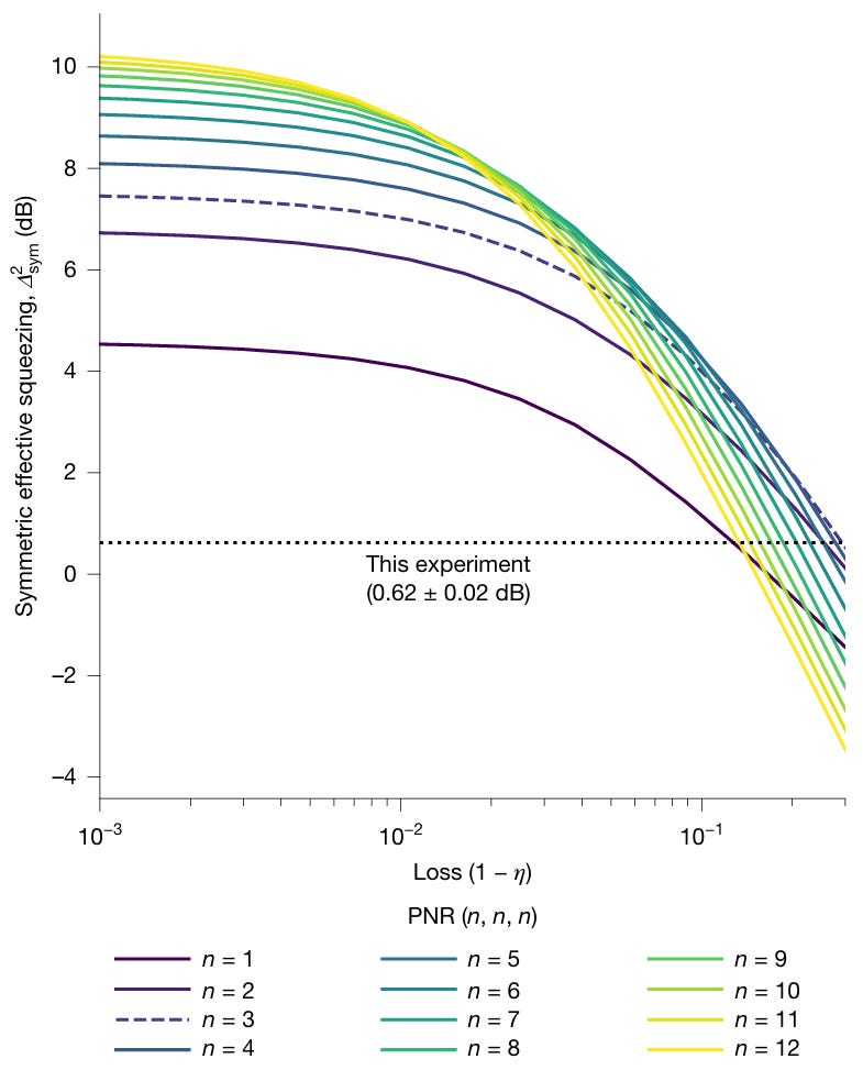
Figure 10: GKP paper p.4 Fig.4. X-axis: end-to-end transmission (0-100%), Y-axis: symmetric effective squeezing (dB). Simulation curves for various PNR patterns plus experimental data points. Horizontal dotted line: fault tolerance threshold 9.75 dB.
Source: “Larsen et al., Nature (2025)”
This graph contains the paper’s central message. Here is how to read it.
How to read the graph: The X-axis is optical loss, with smaller loss (better) toward the left. The Y-axis is GKP qubit quality (effective squeezing, dB), with higher being better. Each colored curve represents simulation results for different PNR detector photon counts (n=1, 2, 3...).
An exam score analogy: the Y-axis is the test score, the X-axis is the noise level in the exam hall. When noise (loss) is high, even a brilliant student (high n) scores poorly. As noise decreases, the more capable students score progressively higher.
Current position: The dotted horizontal line “This experiment (0.62 dB)” is the current experimental result. On the X-axis, loss is 18-22% (toward the right). At this loss level, the n=3 curve (blue dashed) gives the highest squeezing. This is why the paper chose the (3, 3, 3) pattern as optimal.[12] (3, 3, 3) is not the only valid pattern. (2,2,2), (4,4,4) and others are possible too, but after testing multiple patterns, n=3 performed best at the current loss level.
Why the curves cross: There is a critical tradeoff here. Low n is resistant to loss but has a low quality ceiling. High n has a high ceiling but is vulnerable to loss. Look at the far left of the graph (loss ≈ 0): n=1 peaks at ~4.5 dB, n=3 at ~7.5 dB, n=8 at ~10 dB. With n=3, even at zero loss, the threshold (9.75 dB) can never be reached. Crossing the threshold requires n≥8, but higher n means more photons must be detected, and when loss is high, photons disappear en route and the state degrades. Using the orchestra analogy again: a 20-violin chord (high n) is rich, but if the concert hall door (loss) is narrow, most players cannot enter and the chord itself falls apart. A 3-violin chord (n=3) is simpler, but 3 players can make it through even a narrow door.
The core message: Look at the far left of the graph (loss < 0.5%). Curves for n≥8 cross above 9.75 dB, the fault tolerance threshold from the Aurora paper.[12] No new physics is needed. Reducing loss on the same chip is enough. Reducing loss so that n=8 or higher becomes viable is the core of the roadmap.
Simulation results show that when transmission exceeds 99.5%, PNR patterns of the form (n, n, n) with n > 7 produce symmetric effective squeezing above 9.75 dB, crossing the fault tolerance threshold.[12]
Summary:
Current transmission: 78-82% (18-22% loss). Send 100 liters, 78-82 arrive.
Target transmission: >99.5% (<0.5% loss). Send 100 liters, 99.5+ arrive.
Gap: loss must be reduced to approximately 1/40th of current levels. Not impossible in principle, but requires major improvements in SiN process optimization and packaging technology.
Key takeaway: The GKP paper generated optical GKP qubit states on a custom 300mm SiN chip and confirmed a 3x3 negative grid in the Wigner function. Effective squeezing of 0.62 dB vs. a 9.75 dB threshold. The gap is large, but simulations show it can be closed by reducing loss below 0.5%.
6. Closing + Part 2 Preview
Xanadu’s three Nature papers show a single journey:
Borealis (2022): Can photons achieve quantum advantage? → Yes, on a GBS task. But with bulk optics.
Aurora (2025): Can a photonic quantum computer be built on chips and scaled? → Architecturally, yes. But loss is far from threshold.
GKP (2025): Can fault-tolerant qubits be generated on a photonic chip? → The structure is confirmed. But loss must be reduced by 1/40th.
All three converge on the same conclusion. “This technology works. But it is not yet fault-tolerant.” And the gap comes down to one thing: optical loss in photonic devices.
Current Aurora P1 path: 56% loss. GKP chip: 18-22% loss. Fault tolerance threshold: <1% loss. Loss is trending down as the platform evolves from bulk to chip, from 200mm commercial to 300mm custom process. But the gap to the target remains at tens of times.
The next question is: chip-fiber coupling, MZI switches, photodetectors, fiber delay lines. Where does each of these four components stand today, and how far is the target? And where does PsiQuantum, building photonic quantum computers with a completely different approach, stand on the same metrics?
Part 2 covers:
Full device-level analysis (A through J): 10 components from chip-fiber coupling at 0.45 dB to TES efficiency at 99.89%, each with current level, next-gen reported values, and FT targets in one table
Xanadu vs. PsiQuantum 16-row comparison table: same goal, photonic QC, but loss tolerance differs by 10x. Room-temperature QPU vs. full 2K cooling, TFLN vs. BTO, off-chip TES vs. on-chip SNSPD
Scenario-based investment implications: 2029 FT achieved / delayed / GKP approach hits a wall. What happens to XNDU, IONQ, RGTI, and foundries in each scenario
5 key risks + monitoring points
Whether Weedbrook’s 2019 warning about “too much hype” still applies today, or whether the technology accumulated since then justifies the hype, the answer is measured in dB.
References & Sources
[1] The quantum gold rush. Nature 2019.10, quantum tech startup investment analysis
[2] Toronto quantum company Xanadu set to debut on TSX, Nasdaq. Yahoo Finance 2026.3.25, listing coverage
[3] Xanadu Announces SPAC Deal to Go Public. The Quantum Insider 2025.11.3, SPAC deal announcement
[4] Xanadu Quantum (XNDU) Stock Price. Robinhood as of 2026.4.10
[5] Xanadu negotiating with Canadian government for CA$390m. Data Center Dynamics 2026.3, government support and prior investment history
[6] Xanadu reveals government funding talks as company woos SPAC investors. The Globe and Mail 2026.3, includes Weedbrook interview
[7] Crane Harbor Acquisition Corp. - Form 425. SEC Filing 2025.11.24, deal structure details
[8] Canadian quantum firm Xanadu debuts on public markets after SPAC deal. Verdict 2026.3, final proceeds
[9] Xanadu Announces Negotiations Toward Up to CAD $390 Million. GlobeNewsWire 2026.3.11, Project OPTIMISM official announcement
[10] Quantum computational advantage with a programmable photonic processor. Nature 2022.6, Borealis paper
[11] Scaling and networking a modular photonic quantum computer. Nature 2025.2, Aurora paper
[12] Integrated photonic source of Gottesman-Kitaev-Preskill qubits. Nature 2025.6, GKP qubit paper
[16] Xanadu Quantum Technologies. Schedule 13D. SEC filing 2026.4.2, CEO Weedbrook ownership disclosure. 46,432,704 Class A shares (15.58%), 51.8% of Class B on as-converted basis
Disclaimer: This article is an independent, engineering-driven technical analysis published by PhotonCap. All content is based on publicly available information and is intended for educational and informational purposes only. Nothing herein constitutes a recommendation to buy, sell, or hold any security. The author may hold positions in securities discussed and may transact at any time without notice. Readers should conduct their own due diligence before making any investment decisions.
Very technical analysis, but more approachable, than you usual ones for simple user like me.
Brilliantly written! I think for this guy in his 7th decade, after reading it several more times, I'll be up to understanding 10%! But I'm here to learn. Thank You!!