
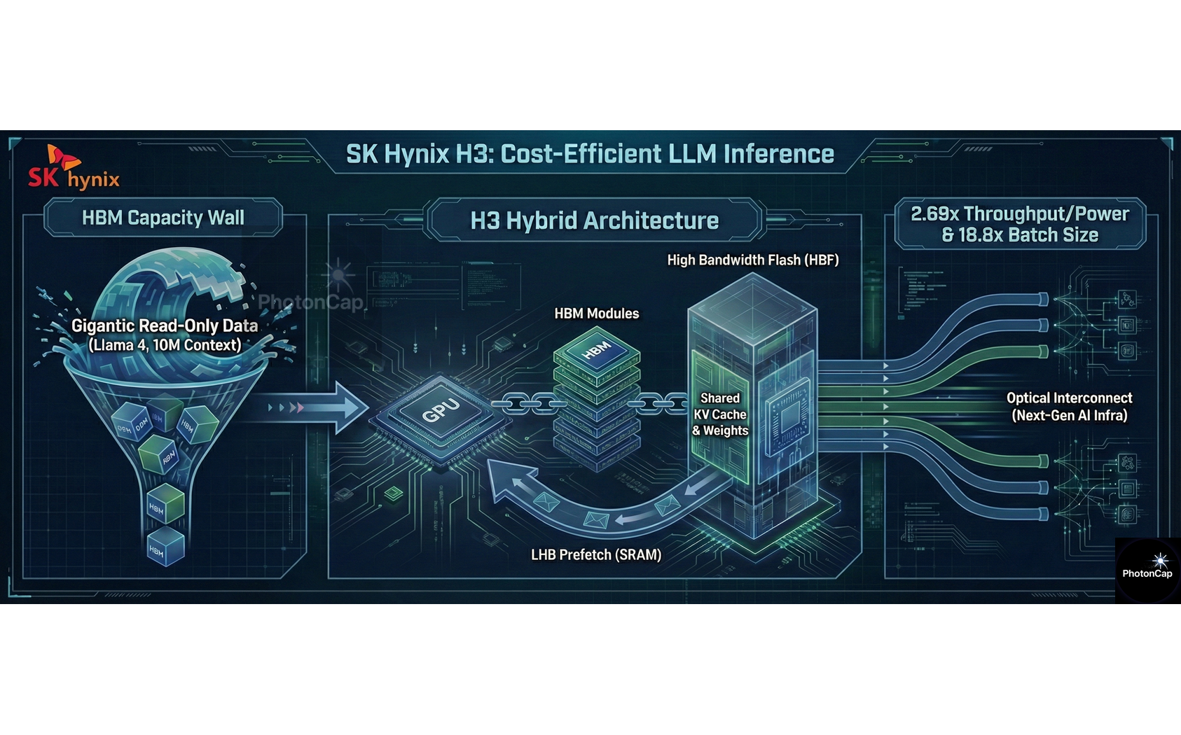
SK Hynix H³: Breaking the HBM Capacity Wall with 'HBF Hybrid’

Summary
As LLM sequence lengths surge to the 10 million (10M) token scale, the shortage of HBM capacity has become a reality. To address this, SK Hynix has proposed the H³ architecture, a hybrid solution combining HBM and High Bandwidth Flash (HBF).
Simulation results prove that this structure achieves 2.69x higher power efficiency and processes up to 18.8x larger batch sizes. A key design element involves resolving slow flash speeds using an SRAM-based Latency Hiding Buffer (LHB).
1. Context: The 10M Sequence Era & The ‘Memory Wall’
(1) The Trend: Llama 4 & 10M Context
Surging Sequence Lengths: The sequence length required for LLM inference is increasing dramatically. Llama 4 is reportedly expected to support sequence lengths up to 10 million (10M).
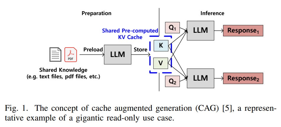
Gigantic Read Load: Processing such long sequences requires massive memory capacity, inevitably leading to Gigantic KV cache reads.
(2) The Problem: HBM Capacity Limits
Insufficient Capacity: The core issue is that HBM capacity is insufficient compared to the rapidly increasing amount of data.
The Bottleneck: Based on the Llama 3.1 405B model, the shared KV cache capacity for a 10M sequence alone reaches 5.4TB, requiring dozens of GPUs just to store the data.
Emergence of an Alternative: To overcome this HBM capacity shortfall, HBF (High Bandwidth Flash) has been proposed.
2. The Device: What is HBF (High Bandwidth Flash)?
(1) Structure & Specs
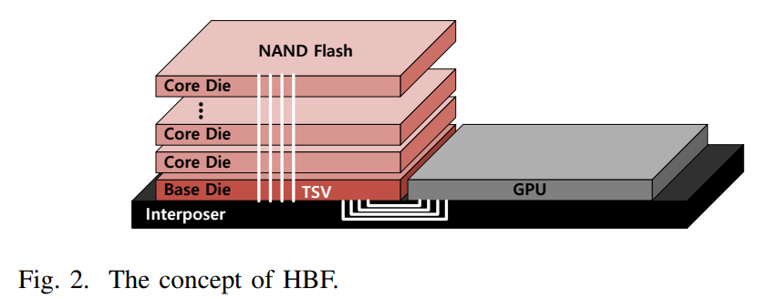
Vertical Stacking: HBF is a next-generation memory device that vertically stacks NAND flash dies and connects the base die and NAND dies using TSVs (Through Silicon Vias) to secure high bandwidth.
Target Specs: It supports bandwidth comparable to HBM, while offering significantly larger capacity than HBM.
(2) Pros & Cons (Trade-off)
Strengths: Offers up to 16x larger capacity than HBM.
Weaknesses: Suffers from longer access latency, lower write endurance, and up to 4x higher power consumption per bit compared to HBM.
3. H³ Architecture: Hardware Design & Data Placement
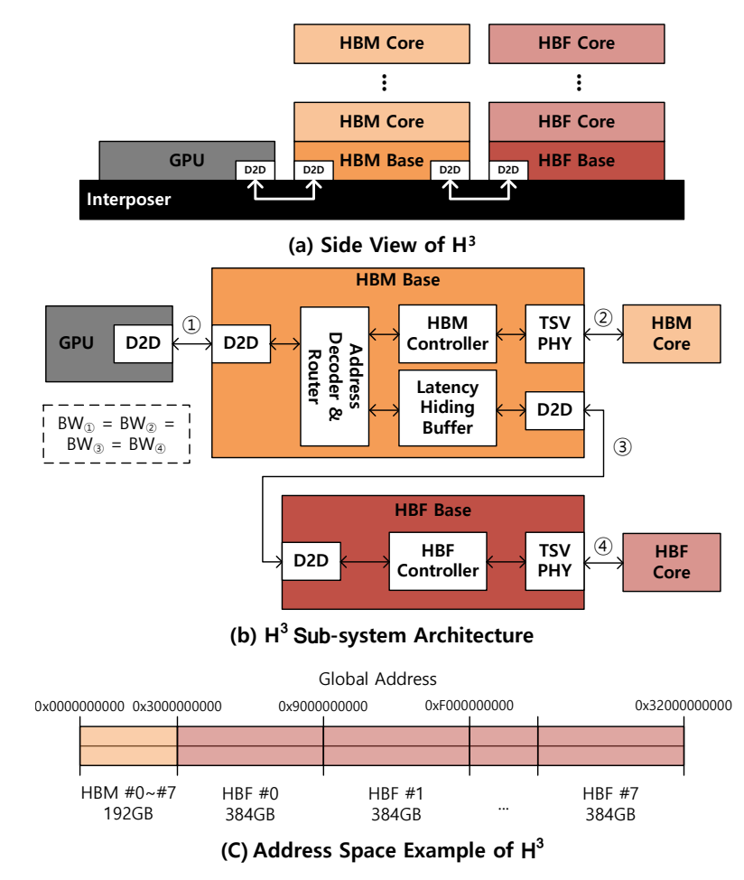
(1) Topology: Daisy-Chained Connection
Daisy-Chain Method: Due to limited physical space (Shoreline) on the GPU, HBF cannot be attached directly. Instead, HBM and HBF are connected in a series (Daisy-chained) configuration.
Connection Order: GPU ↔ HBM Base Die ↔ HBF Base Die (via D2D Interface).
Unified Address Space: From the GPU’s perspective, HBM and HBF are recognized as a single main memory with a unified address space.
(2) Data Placement Strategy
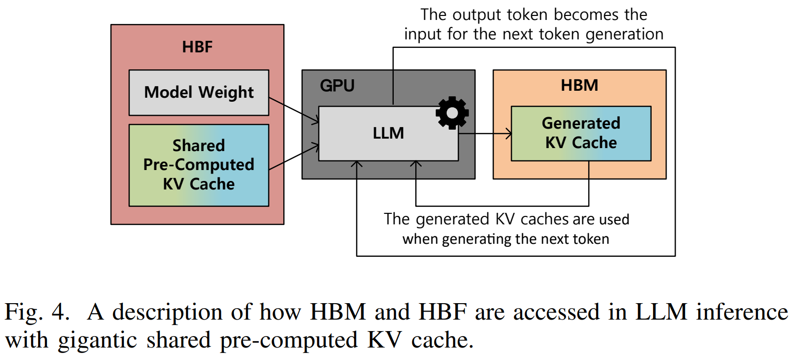
Utilizing HBF (Read-Only): The Shared pre-computed KV cache and Model Weights, which are inherently read-only, are stored in the HBF. This mitigates the issue of HBF’s low write endurance.
Utilizing HBM (Read/Write): The real-time Generated KV cache and other frequently accessed data are stored in the high-speed HBM.
4. Critical Engineering: LHB (Latency Hiding Buffer)
(1) Why LHB? Deterministic Nature
Deterministic Patterns: LLM inference processes layers sequentially, meaning the data required for the next computation is pre-determined.
Latency Hiding: Leveraging this characteristic, an LHB (Latency Hiding Buffer) is integrated into the HBM base die to compensate for the long latency of NAND flash.
(2) Feasibility Check: Can it fit on the chip?
Capacity Calculation: Assuming double buffering, the required LHB capacity formula is:
\($Capacity_{LHB} = 2 \times BW_{HBF} \times Latency_{HBF}\)Value Substitution: With an HBF bandwidth (BW_{HBF}) of 1TB/s and latency (Latency_{HBF}) of 20µs (based on SLC NAND), the required capacity is calculated to be 40MB.
Silicon Area Verification: Calculating the area for a 40MB SRAM core based on 3nm process SRAM density (0.021μm²):
\((40 \times 10^{6} \text{ bytes}) \times 8 \frac{\text{bits}}{\text{byte}} \times 0.021 \frac{\mu\text{m}^{2}}{\text{bit}} \times \frac{1 \text{ mm}^{2}}{10^{6} \mu\text{m}^{2}} = 6.72 \text{ mm}^{2}\)Final Overhead: Including a 20% overhead for additional circuitry, the total area is estimated to be 8.06mm². This is approximately 6.7% of the current HBM base die area (121mm²), which is considered an acceptable value.
5. Experimental Results: Overwhelming Efficiency & Scalability
(1) Experimental Setup
Simulation Environment: Since HBF is under development, an in-house simulator based on analytical modeling was used.
Model: Llama 3.1 405B (1M & 10M Sequence).
Hardware: NVIDIA B200 GPU + HBM3e (192GB, 8TB/s).
HBF Spec: Capacity 3TB, Bandwidth 8TB/s, Power 160W/cube (vs. HBM 40W/cube).
(2) Key Results
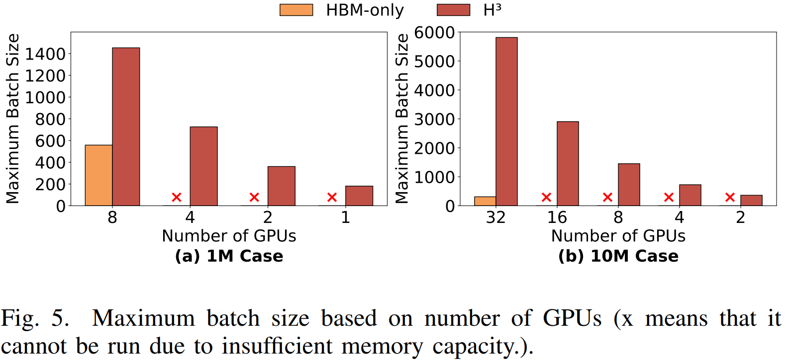
Scalability (Batch Size):
1M Case: H³ allows for batch sizes up to 2.6x larger than HBM-only.
10M Case: H³ allows for batch sizes up to 18.8x larger. (HBM-only requires 32 GPUs, whereas H³ runs on just 2 GPUs) .
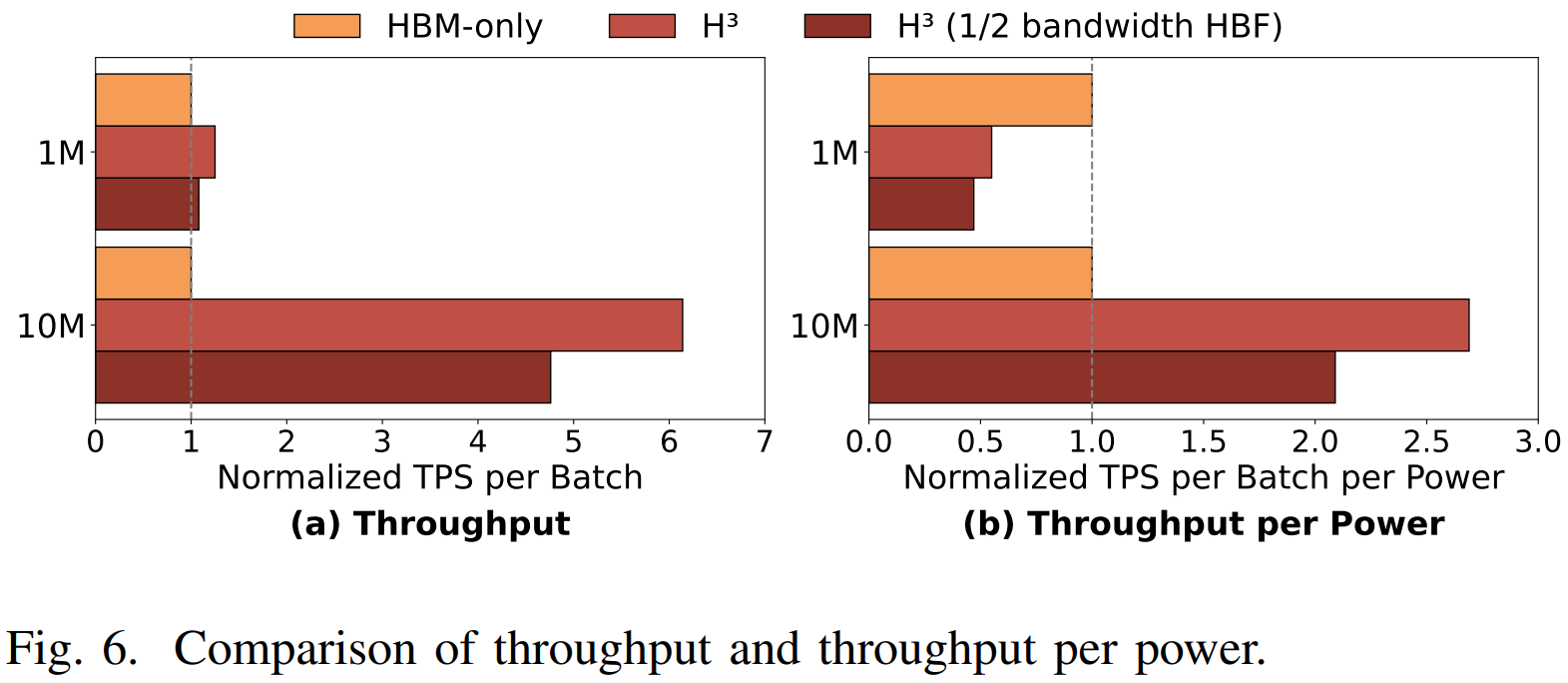
Cost Efficiency (Throughput per Power):
Throughput increased by 6.14x in the 10M case.
Despite HBF’s higher power consumption, the Throughput per Power is up to 2.69x higher.
Robustness:
Even with HBF bandwidth halved, the power efficiency in the 10M case remains 2.09x higher.
PhotonCap’s Insight
This paper strongly suggests that the H³ architecture is a cost-effective solution for LLM inference dealing with gigantic Read-Only data. While the reliance on 100% simulation and analytical modeling rather than actual silicon data is a limitation, the authors secured the legitimacy of their results by proving performance superiority even under a “worst-case scenario” (halved HBF bandwidth).
However, a critical perspective on Scale-out is necessary. The paper posits that 10M sequence processing requires at least 32 GPUs, assuming an InfiniBand-based network for connection. Yet, current InfiniBand connections for short distances within data centers still rely heavily on Copper (DAC) cables. It is at this juncture that the combination of the H³ architecture with Optics becomes technically indispensable for data center-level expansion.
First, as the H³ architecture increases the data processable per GPU to the terabyte scale, existing copper-based InfiniBand connections face physical limitations. In a scenario where multiple nodes must share or transmit terabytes of KV cache data, electrical signal-based transmission suffers from severe signal attenuation and limited bandwidth scalability as distance increases. To process this explosively grown data without bottlenecks and secure the true benefits of scale-out, the full-scale introduction of Optical technology, capable of high-bandwidth transmission free from copper’s distance constraints, must precede.
Furthermore, low-power Optical I/O is required to maintain the 2.69x power efficiency achieved by H³ at the system level. Even if power efficiency is improved at the memory tier via HBF, the total TCO (Total Cost of Ownership) improvement will be negated if high-speed copper interconnects consume excessive power during inter-node data transmission. To extend the power efficiency secured within the node to the entire data center, Optical I/O solutions with significantly lower power consumption per bit compared to electrical methods must be integrated.
Ultimately, for the future AI infrastructure to evolve into a CXL (Compute Express Link)-based Memory Pooling structure—where hybrid memory like H³ is utilized as a massive shared resource beyond the rack unit—Optical technology is essential. Moving beyond direct connect structures tied to individual GPUs, CXL over Optics technology will be the foundational support allowing low-latency access to physically distant HBF pools, completing the next-generation AI infrastructure architecture.
🔗 Reference:
M. Ha, E. Kim and H. Kim, “H³: Hybrid Architecture Using High Bandwidth Memory and High Bandwidth Flash for Cost-Efficient LLM Inference,” in IEEE Computer Architecture Letters, doi: 10.1109/LCA.2026.3660969.
HBF & Optics Insight: HBF (High Bandwidth Flash) and Optics: The Missing Link in AI Infrastructure (Author’s Article)