
Samsung's Silicon Photonics Bet: Too Late Against TSMC, GFS and Tower?
One foundry is already shipping $380M/year in SiPh. Samsung has zero. Inside the race to build the optical backbone of AI.

Samsung’s Silicon Photonics Bet: Too Late Against TSMC, GFS and Tower?
One foundry is already shipping $380M/year in SiPh. Samsung has zero. Inside the race to build the optical backbone of AI.
At OFC 2026, Samsung Foundry publicly announced its entry into the silicon photonics (SiPh) foundry market with a 300mm platform. The roadmap targets optical engines in 2027 and turnkey CPO services by 2029. This article builds on the technical analysis from Part 1 to examine the competitive landscape of the SiPh foundry market, assess whether Samsung’s vertical integration strategy (HBM + foundry + packaging + SiPh) offers genuine differentiation, and analyze the investment implications across four foundry players.
Contents
Why Samsung Entered Silicon Photonics
SiPh and CPO: Why Foundries Matter
Samsung’s Technical Position: What They Showed, What’s Missing
The Real King of SiPh Foundry Is Not Who You Think
Vertical Integration: What Do Customers Actually Want?
Investment Implications: Scenario Analysis and Monitoring Points
Closing
References & Sources
1. Why Samsung Entered Silicon Photonics
Samsung Foundry’s revenue sits at roughly one-sixth of TSMC’s (around $15-18B vs. TSMC’s $90B+ as of 2025). Competing on advanced logic nodes alone will not close that gap. On March 17, 2026, at OFC 2026 in Los Angeles, Samsung Foundry opened a new front. The company officially declared its entry into the SiPh market with two conference papers.[1][2]
Samsung’s roadmap looks like this: PIC production readiness in 2026, optical engines based on TC (thermo-compression) bonding in 2027, hybrid bonding transition in 2028, and turnkey CPO (co-packaged optics) services starting in 2029.[5]
The core message Samsung is pushing: “TSMC does not manufacture memory itself. Samsung can offer HBM, foundry, packaging, and SiPh under one roof.”[12] (TSMC does, however, integrate external HBM through its CoWoS advanced packaging.) This is the central logic behind Samsung’s SiPh strategy.
It is an appealing pitch. If you imagine the end state of an AI chip package, with GPU + HBM + optical engine inside a single package, having one company build all of it certainly simplifies the supply chain.
But this market is not an empty field. Where Samsung is trying to enter, there are players already running production lines, securing customers, and generating revenue. And the gap between them is not measured by “a few more GHz.”
This article examines Samsung’s technical position, the real competitive structure of this market, and the conditions under which Samsung’s vertical integration strategy could actually work.
2. SiPh and CPO: Why Foundries Matter
AI clusters are scaling fast. As GPU counts expand from tens of thousands to hundreds of thousands, the copper wiring connecting chip to chip is becoming the bottleneck. Power consumption keeps rising, bandwidth is hitting limits, and latency is not improving.
SiPh is the technology that sends data using light instead of electricity. If copper wiring is a two-lane road, SiPh is an eight-lane highway at half the cost. At link distances above 10 meters, power efficiency runs 5-10x better than copper. Add WDM (wavelength division multiplexing), which sends multiple channels on a single optical fiber simultaneously, and bandwidth scaling becomes straightforward.
CPO takes this one step further. Today, switch chips and optical modules are physically separated. You have probably seen pluggable transceivers at the front of a server rack. CPO puts the optical engine directly inside the switch chip package. Shorter signal paths mean lower power loss and lower latency.
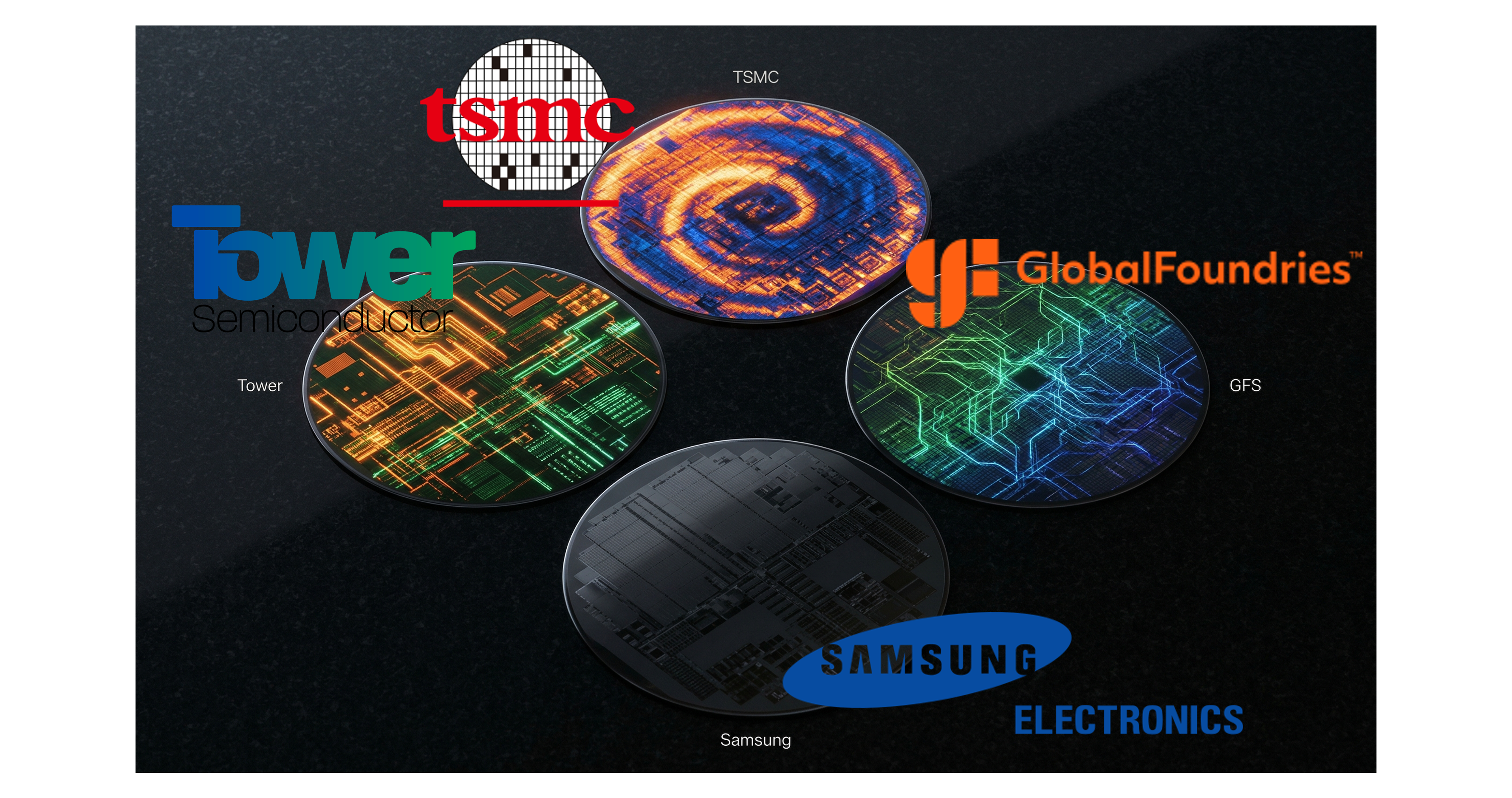
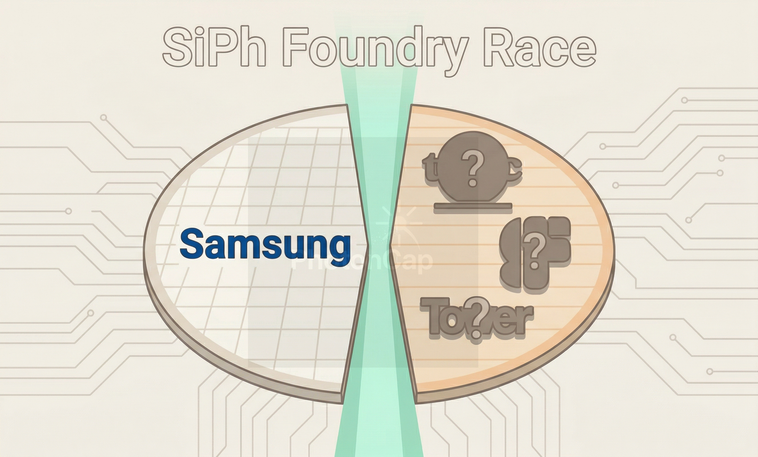
The key point here: building SiPh PICs is not the same as standard semiconductor manufacturing. Handling light requires waveguides (channels that guide light), modulators (devices that convert electrical signals to light), and photodetectors (devices that convert light back to electricity). The number of foundries in the world that can fabricate these on 300mm silicon wafers in a CMOS-compatible process can be counted on one hand. As dedicated SiPh foundries, Tower Semiconductor and GlobalFoundries lead. TSMC has entered with its COUPE platform. STMicroelectronics also started running a 300mm SiPh platform. Samsung is trying to become the fifth.
The SiPh foundry market has risen rapidly as a critical link in the AI data center interconnect supply chain. At GTC 2025, NVIDIA announced photonics-based versions of its Spectrum-X (Ethernet) and Quantum-X (InfiniBand) switches built on TSMC COUPE.[5] When the most important customer in AI infrastructure declares “we are connecting with light,” foundries follow.
The SiPh foundry market is, at its core, a race to build the factories that supply light to AI data centers.
3. Samsung’s Technical Position: What They Showed, What’s Missing
Here is a summary of Samsung’s two OFC 2026 papers. Detailed device-level analysis was covered in Part 1[3], so this section focuses on key specs and context.
What They Showed: Device Performance
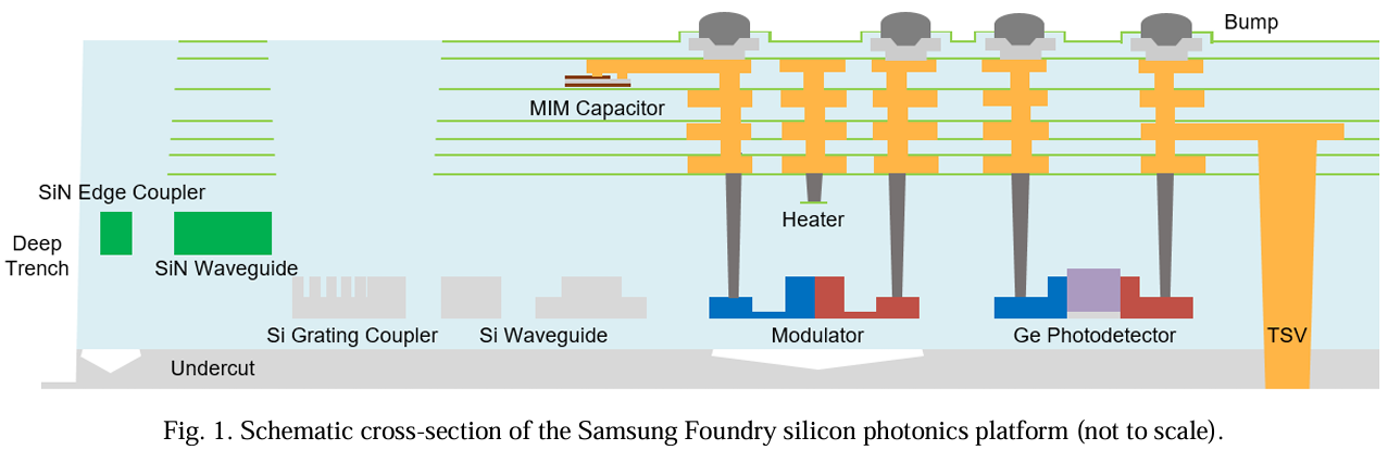
Samsung’s 300mm SiPh platform (Tu2D.3 paper) integrates Si and SiN dual waveguides, Ge photodetectors, TSVs (through-silicon vias), heaters, and MIM capacitors on an SOI (silicon-on-insulator) wafer.[1]
Key device specs:
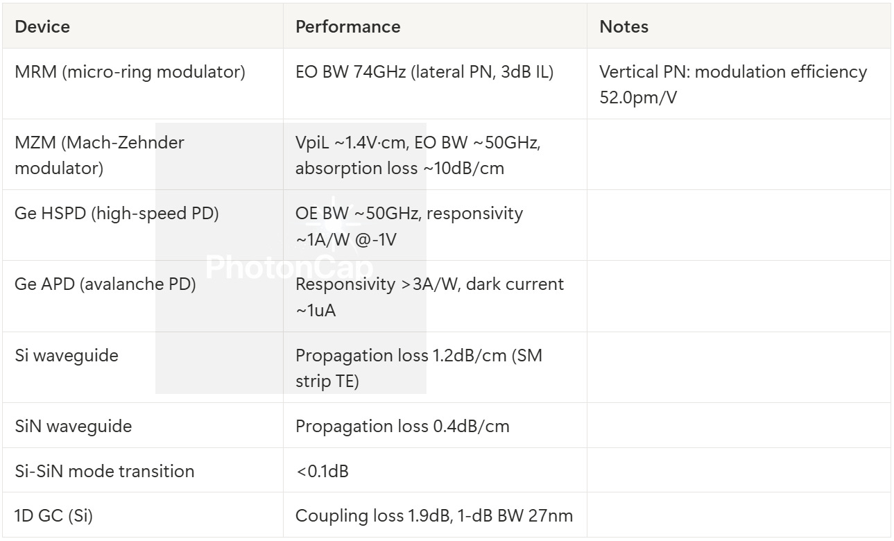
The MRA-Ge APD (microring-assisted Ge avalanche photodiode), published as a separate paper (Th3F.6), is also notable. Using a microring resonator, Samsung achieved 0.82A/W on-resonance responsivity (@-1V), avalanche gain of 7.5 (@-6.1V), and a gain-bandwidth product of 253GHz (@-6.5V) from a Ge APD with a 180nm x 400nm footprint.[2] Compared to conventional SACM APDs that require 10-15V or more, -6.1V is genuinely lower. However, as analyzed in Part 1, within a CPO package where EIC power rails run at 0.75-1.8V, a separate voltage converter is still required.[3]
The PDK is also in place: over 40 device models, DRC/LVS/PEX verification decks, temperature-dependent modeling from 25-85C, and model-hardware correlation covering MRM self-heating and optical peaking effects.[1]
imec separately measured Samsung’s modulator at 224Gbps/lane, as reported by The Elec.[12] This number aligns with 200G/lambda targets, enabling 1.6Tbps with an 8-lane configuration.
What’s Missing: System Integration and Customers
No system-level integration data. Samsung’s OFC papers are entirely device-level characterization. There is no data showing a PIC and EIC bonded together and operating as an optical engine. The 50Gbaud PAM4 eye diagram is simulated, not measured.[1] No optical link transmission experiments. No multi-lane or WDM data.
No production customers. Broadcom SiPh collaboration has been reported since March 2025[4], and Samsung has identified optical module companies like Coherent and Lumentum, along with fabless PIC design firms, as potential customers.[12] But as of OFC 2026, no specific design win has been disclosed.
No production track record. PDK 1.0 is ready, but Samsung has zero history of taking customer designs through to volume production. In the foundry business, “having a PDK” and “having validated production yield” are entirely different milestones.
One more piece of context: Samsung’s SOI wafer uses a 305nm Si layer thickness.[1] The most widely used thickness for datacom PICs is 220nm (though 300nm is used in RF photonics, and 400nm in nonlinear photonics). As noted in Part 1, this non-standard thickness introduces optical mode optimization tradeoffs and PDK compatibility questions.[3] Porting existing 220nm-based designs to Samsung’s platform may require redesign.
Samsung’s device physics are competitive. MRM 74GHz, MZM VpiL 1.4V·cm meet foundry-grade benchmarks. What is missing is system integration, production track record, and customers.
The Gap Samsung Needs to Close
The TSMC gap is the place to begin. TSMC announced COUPE (Compact Universal Photonic Engine) in 2024, completed pluggable qualification in 2025, and is targeting CoWoS-based CPO production qualification around 2026.[5] NVIDIA’s announced Spectrum-X Photonics and Quantum-X Photonics switches are planned on the COUPE platform.
There is a real technical difference as well. TSMC COUPE uses SoIC-X, a 3D stacking technology that bonds the EIC on top of the PIC using Cu-Cu hybrid bonding. Cu-Cu hybrid bonding is the “bumpless” approach: instead of solder bumps, copper pads on each die are polished flat and bonded directly at the atomic level. SoIC-X is the high-performance variant of TSMC’s 3DFabric platform, with bond pitch below 9um and a roadmap to 3um in future generations. This minimizes impedance at the electrical-optical interface.[5]
Samsung’s first optical engine in 2027 will use TC bonding, with Cu-Cu hybrid bonding arriving in 2028. Here is why that difference matters:
TC (thermo-compression) bonding: Uses solder bumps melted together under heat and pressure. Bump pitch is typically 40-100um. Connection density is limited, and signal paths are longer due to bump height.
Cu-Cu hybrid bonding: Copper pads bonded directly at the atomic level. No bumps, so pitch can shrink below 10um. Connection density is 10x or more compared to TC. Signal paths are extremely short, reducing impedance and power loss.
The analogy: TC is gluing blocks with adhesive. Cu-Cu hybrid bonding is polishing surfaces flat and welding them directly. The latter is far denser and more robust, but the process is harder to execute. TSMC is already in production with SoIC-X. Samsung will not reach this stage until 2028. The gap: one to two packaging technology generations.
In December 2025, Alchip and Ayar Labs demonstrated a COUPE-based optical connectivity solution at TSMC’s European OIP Forum.[8] The demo showed a 100Tb/s in-package optical I/O engine with UCIe interface, the industry’s first public demonstration of PIC+EIC operating on the COUPE platform. Samsung has not reached this stage yet.
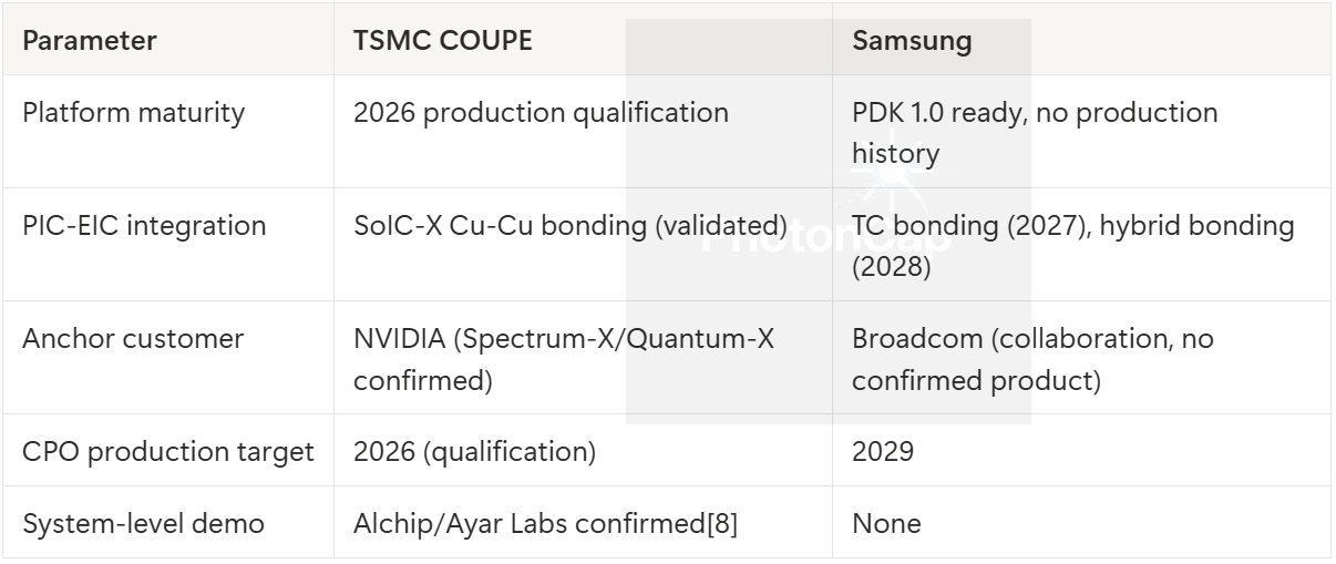
Against TSMC alone, the gap is three years. Catching TSMC head-on is not realistic for Samsung.
But there is a missing variable here. TSMC is the “most advanced” SiPh player, but it is not the “largest” SiPh foundry by revenue.
And once you understand why that other company’s position is more defensible than Samsung’s, you start to see where the real money is made in this market.
