
[PC101] Lecture 3: Traffic Control for Light: Waveguides and Passive Devices

“The devil is in the details.”
Welcome. This is PhotonCap.
In Lecture 2, we learned how to lease the massive factory known as the CMOS process. Now, it is time to dig the ‘canals’ for light to travel through within that factory, and to arrange the ‘sluice gates and puddles’ that divide and merge the flow of water.

https://substack.com/@photoncap/p-186512199
In the world of Silicon Photonics, these ‘details’ are synonymous with survival. Even without a power connection, Passive Devices—which control water (light) purely through their structure—are the foundational infrastructure occupying over 80% of the chip area. In this realm, where a margin of error of just 1nm manifests as the devil known as ‘Loss,’ we will now dive into the sophisticated design engineering of passive devices.
💡 [Mental Model] Excavating Water Channels in a Playground
Before getting into the technical explanation, let’s picture a dirt playground in our minds.
From now on, we are going to dig channels (Waveguides) into this dirt floor (Silicon Wafer) with our fingers and let water (Light) flow through them.
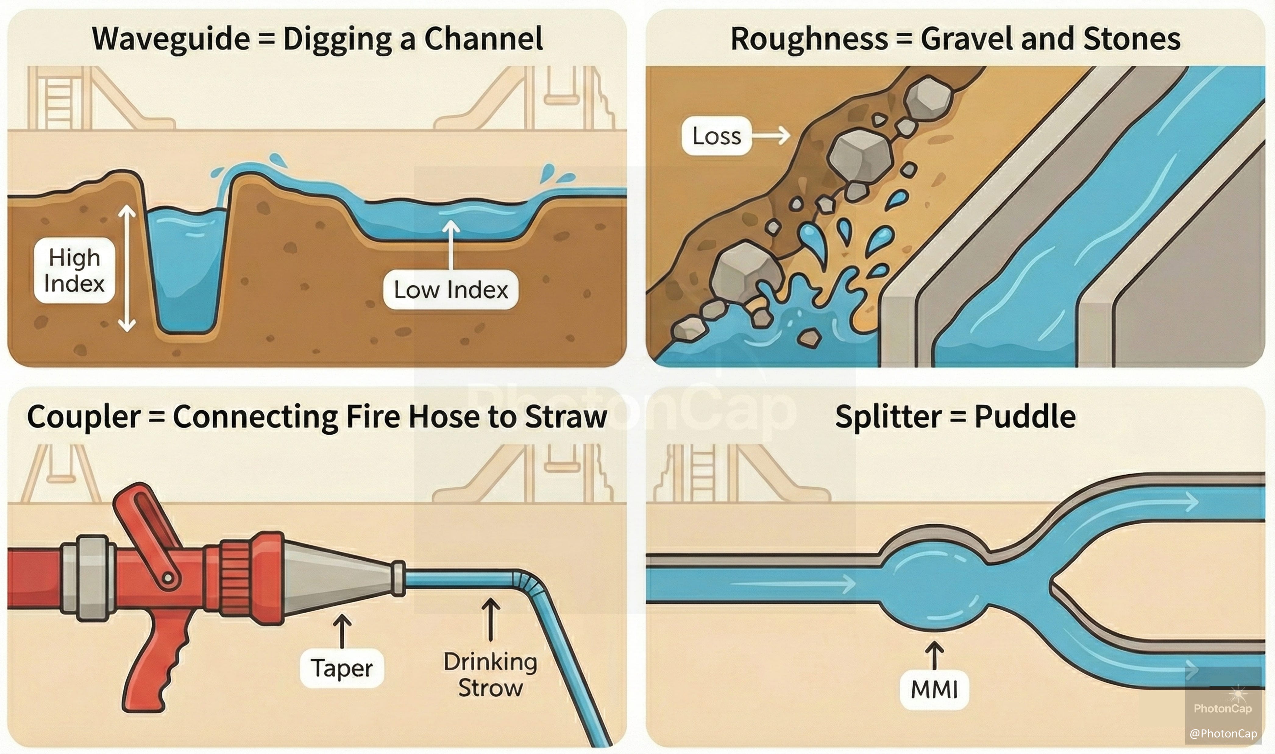
Waveguide = Digging the Channel: We dig the dirt with our fingers. If we dig deeply (High Index), the water doesn’t spill over, allowing for sharp turns. If we dig shallowly (Low Index), the water feels the rough sides less and flows comfortably with less loss, but it overflows easily.
Roughness = Pebbles and Gravel: If pebbles and rough soil stick out from the channel walls, the water hits them and splashes everywhere. This is exactly what Loss is. Like a master plasterer, we must smooth it out to send the water to the end without losing it.
Coupler = Connecting a Firehose to a Straw: The external water tank (Optical Fiber) is the size of a firehose, but the channel I dug (Chip) is only the size of a straw. If you just connect them, water will leak everywhere. Therefore, we need a funnel (Taper).
Splitter = Puddles and Two Channels: When splitting the water flow, if you force a narrow Y-shape, the soil collapses due to the water pressure. If you dig a small puddle (MMI) in the middle, the water pools briefly and then naturally divides into two paths.
1. Waveguide: The Road Where Light Travels
Just as electrons ride copper wires, light travels along roads called Silicon Waveguides.
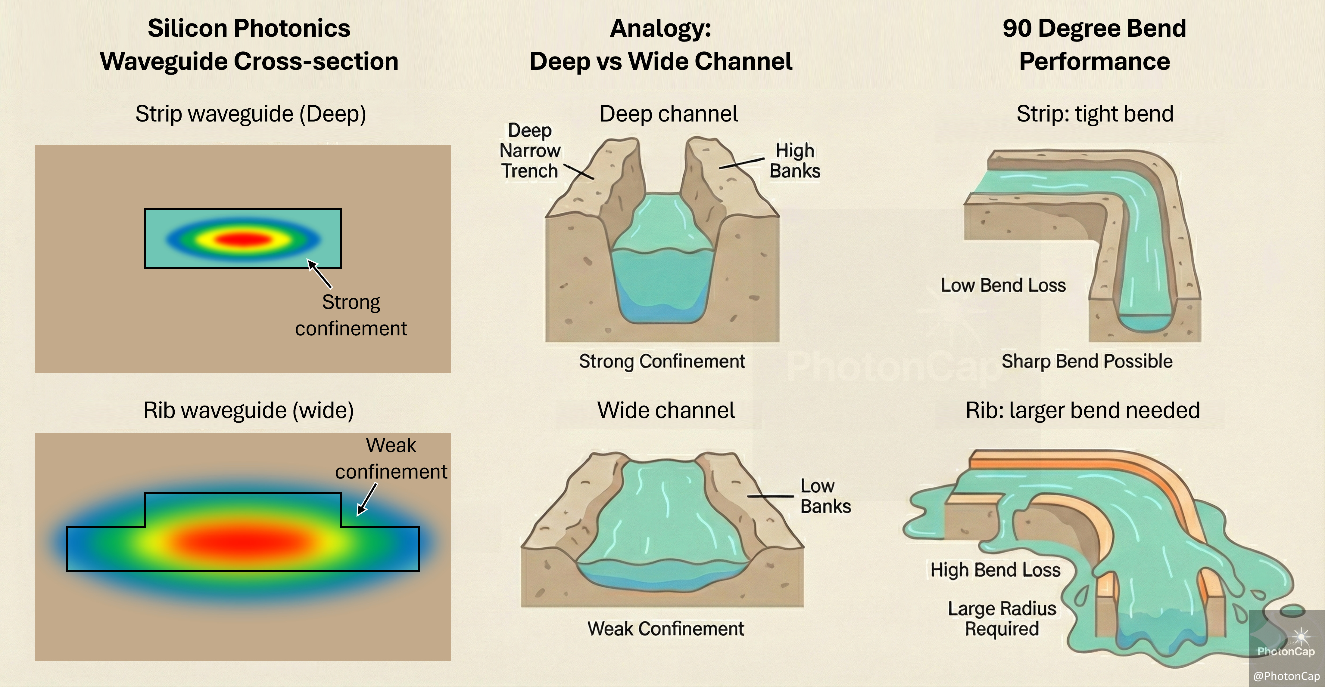
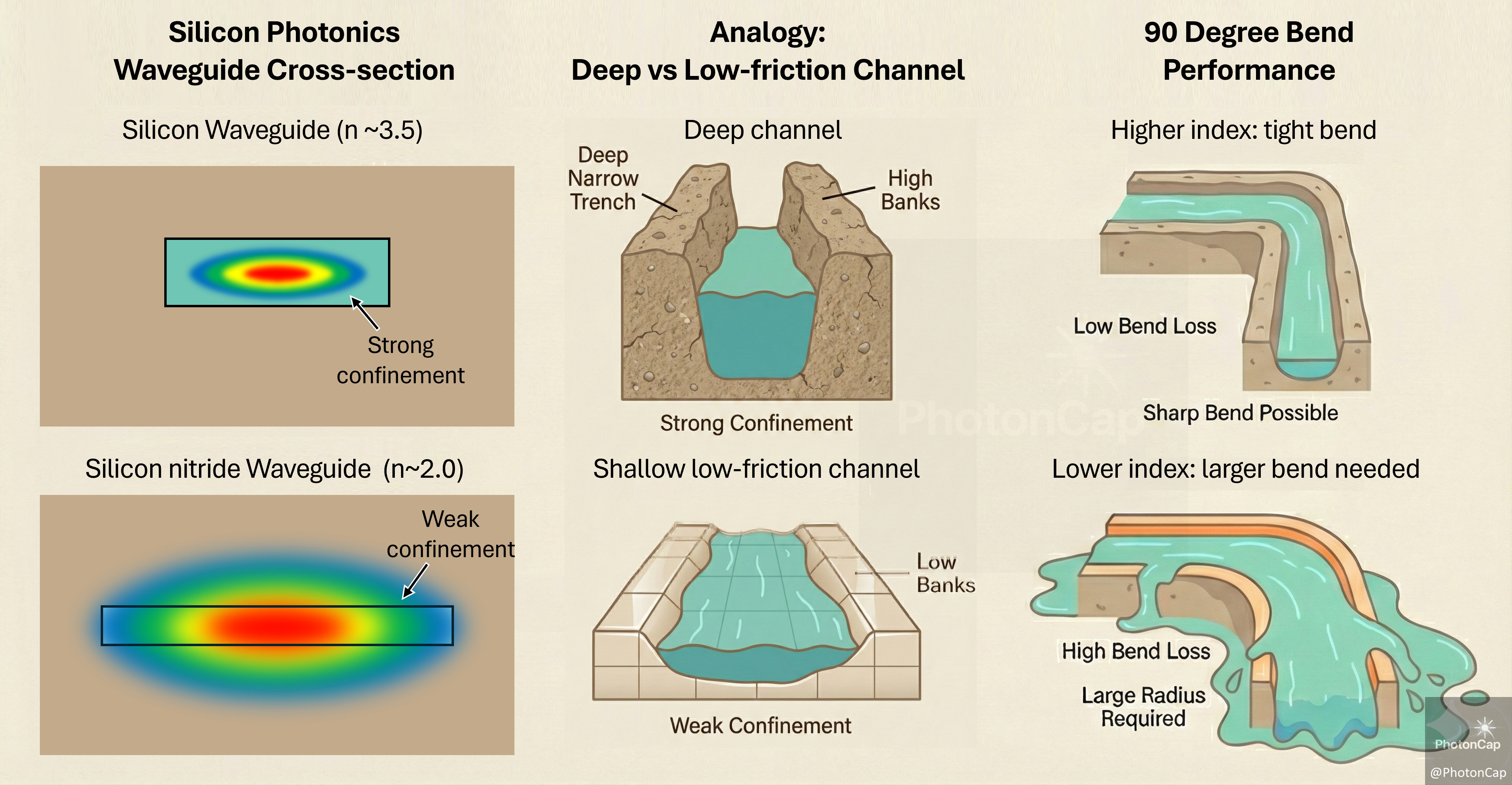
Strip Waveguide: Created by etching the silicon layer all the way to the bottom. Because it confines light strongly, it is advantageous for sharp curves (allowing for a smaller footprint).
Rib Waveguide: Created by leaving a thin layer of silicon. Because the width where light travels is wider (a wider lane), the optical loss is lower, but it requires additional process steps and masks (to define the Rib).
Propagation Loss: When laying a highway, the most important thing is the smoothness of the asphalt. The capability of a Silicon Photonics Foundry (process) and Fabless (design) company is proven by a report card measured in dB/cm. If the wall surface is rough by even 1nm, the light bounces off. Controlling this scattering loss is the core know-how of foundries and fabless companies.
💡 [Analogy: The Importance of Plastering]
Imagine fist-sized rocks embedded in the walls of a bobsled track. Every time the sled hits one, it loses speed and bounces. The foundry’s Etching process is like a plastering job that smooths these bumpy walls to be as reflective as a mirror.
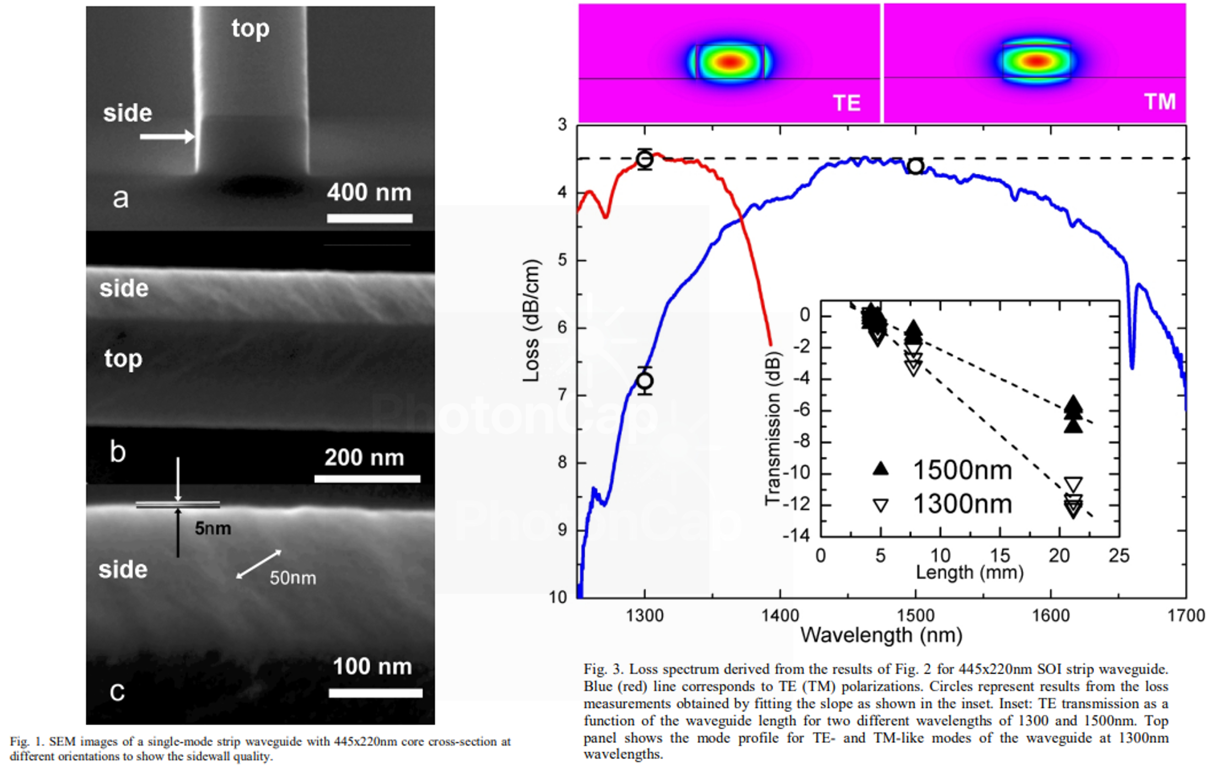
In 2004, IBM’s Dr. Vlasov and team published a paper in Optics Express proving that silicon waveguides could achieve low enough loss for commercialization, shocking the industry. Since then, every company has staked its life on “polishing the walls like mirrors.”
Silicon’s Weapon, the ‘Sharp Turn’: Conventional optical fibers leak light if you bend them. However, silicon has a large refractive index difference between the silicon defining the waveguide and the surrounding glass (SiO2), so the light is strongly confined. (To use a simple analogy, it’s hard for a frog in a deep well to jump out.) Light turns well even with a 5µm (micrometer) radius. This is the key to drastically reducing chip size (High Integration).
💡 [Analogy: Deep Canal vs. Shallow Stream]
A Strip is a channel dug deep into the ground. The banks are high, so the water doesn’t overflow, allowing for sharp turns. However, the path is narrow, so the water hits the rough walls frequently.
Conversely, a Rib is like scraping off just the top layer of soil to form a wide, shallow stream. The water feels the walls less and flows comfortably (Low Loss), but if it meets a sharp turn, it spills right over the shallow banks.
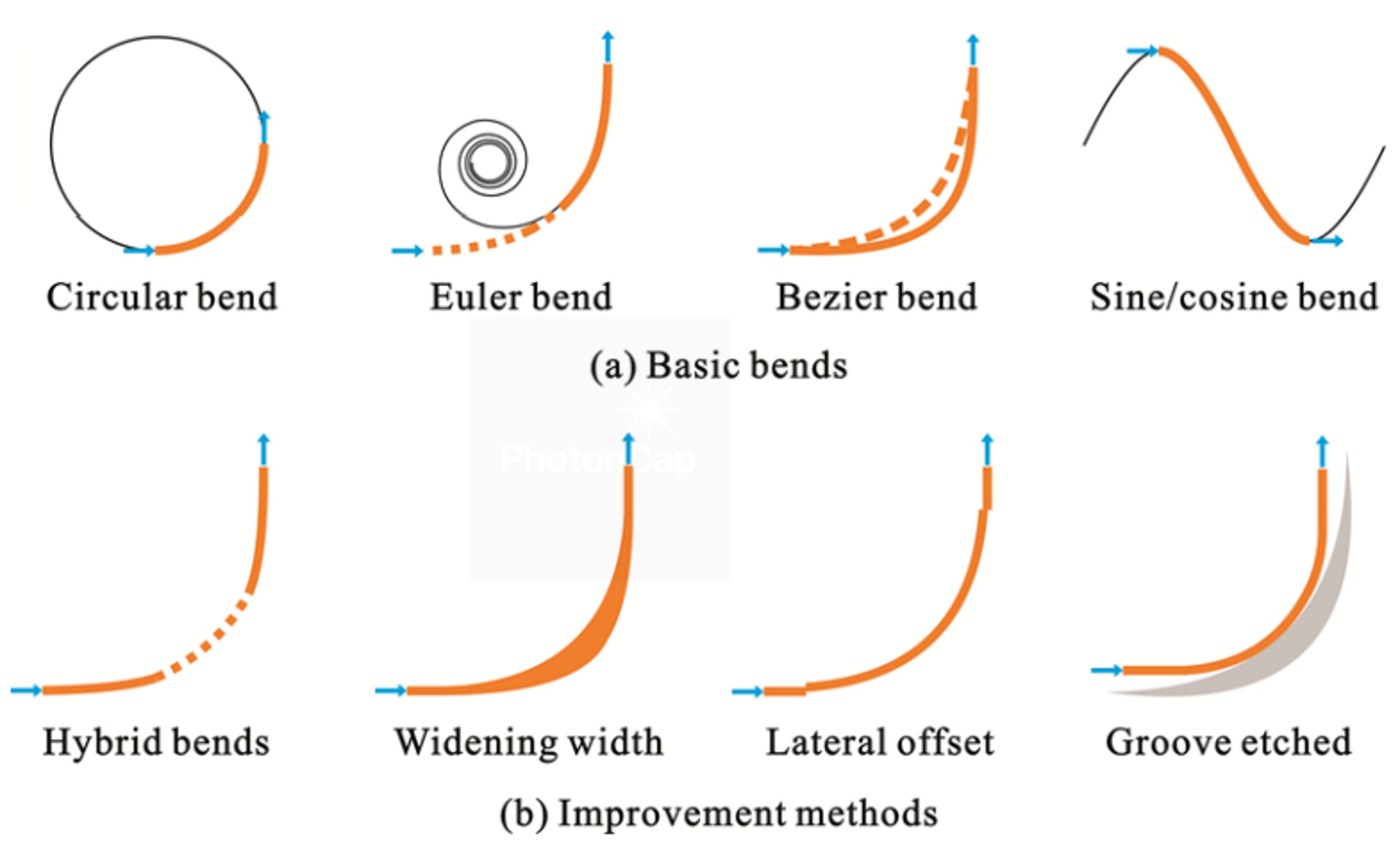
Special Bends for Low-Loss Sharp Turns: Euler Bend
While silicon waveguides allow for sharp turns due to the high refractive index difference, Mode Mismatch Loss occurs at the point where a straight waveguide meets a circular bend due to the mismatch in mode profiles. To suppress this, structures with variable curvature like the Euler Bend are adopted. An Euler bend has a Clothoid curve structure where the curvature changes linearly and gradually from the straight section (curvature 0) to the peak of the curve. This allows the light inside the waveguide to pass through smoothly without sudden mode changes that lead to high-order mode loss or scattering. This is a crucial design detail that determines the level of process optimization in a foundry’s PDK.
💡 [Analogy: Turn the Steering Wheel Slowly]
If you are driving at 100km/h on a highway and suddenly yank the steering wheel 90 degrees, the car will flip. An Euler Bend is a ‘transition curve’ that, when entering a curve from a straight line, starts turning the wheel very slowly and reaches maximum turn at the apex. It allows the water (light) to turn smoothly without being startled.
Evolving Bend Technologies
Beyond Euler bends, research is ongoing into mathematically optimized Bezier Bends, Hybrid Bends mixing different refractive indices or structures, and various techniques like adjusting waveguide width or adding offsets to reduce loss. As seen in the figure below, optimized bend structures ensure that light (Electric Field) flows stably without deviating from the center of the waveguide, even in sharp curve sections.
SiN (Silicon Nitride) Waveguide: A material gaining a lot of attention recently to reduce this propagation loss is the Silicon Nitride (SiN) waveguide. Silicon uses a high refractive index to confine light strongly, but this causes it to hit the walls frequently, resulting in high loss (about 1~2 dB/cm). In contrast, SiN, with a relatively lower refractive index, holds the light more loosely, resulting in drastically lower loss (under 0.1 dB/cm, more than 10x the efficiency of silicon).
However, because it holds light loosely, light can leak out, meaning loss can be high on curved roads rather than straight ones. Therefore, sharp turns are difficult, and a large curvature radius is required (10µm-20µm radius or more).
💡 [Analogy: Tiled Water Channel]
If Silicon is a bumpy dirt floor, SiN is a shallow yet smooth tiled floor. So even if you dig shallow and wide, the water flows very well. This creates an effect similar to the Rib structure explained in Silicon, but creates a wide, shallow stream without the “scraping” effect. The water flows very comfortably, but if it meets a sharp turn, it pours over the shallow banks.
Recently, foundries are stacking these two roads into two layers (Hybrid), establishing a ‘Hybrid Road Network’ where sharp turns and light control are handled by high-refractive-index Silicon, and low-loss straight driving is handled by low-refractive-index SiN. Or, they are designing/processing primarily with SiN. (see 2.2. Evanescent coupling)
💡 [Analogy: 2-Story Highway]
Si (1st Floor): A narrow, winding alleyway. You can get right to the front door of the house (device), but it’s congested and slow.
SiN (2nd Floor): An open highway. You can drive far without traffic lights and without loss.
So, recent chips run long distances on the 2nd floor (SiN) and use a hybrid interchange to come down to the 1st floor (Si) near the destination.
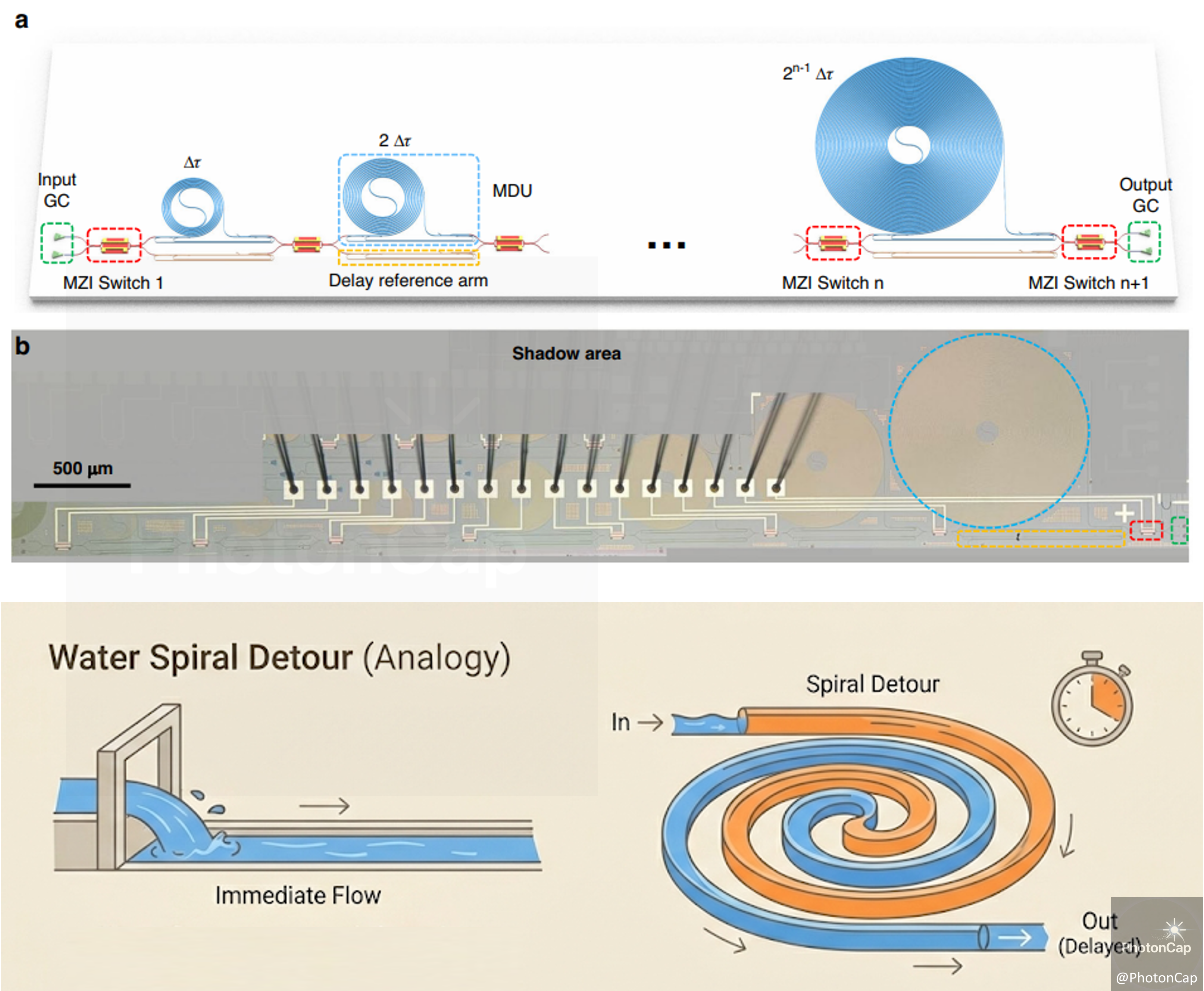
Parking Lot to Briefly Hold Light: Optical Delay Line
There is a technology made possible by ultra-low-loss waveguides like SiN. It is ‘Optical Memory’ or a ‘Delay Line’. Waveguides are wound tightly in a spiral shape for several meters on the chip. While light travels through this long road, its arrival time is delayed, which is used to change the order of signals or create a buffering effect.
💡 [Analogy: Spiral Detour for Water]
Sometimes it’s problematic if water pours out as soon as the floodgate opens. You want to hold the water for a moment, but water cannot stop (stagnate).
In this case, instead of a straight channel, we make a very long ‘Spiral Detour Channel’ that loops around like a track field. The water keeps flowing without stopping, but because it’s going around in circles, its arrival at the destination is delayed.
[Key Company]
ASML (Drawing): Must draw the edges of the waveguide as smoothly as if cut with a knife. (LER Control)
Lam Research & AMAT (Carving): This is the battleground. Standard semiconductor processes (Bosch) leave ripple patterns on the walls. Dedicated photonics recipes must be used to carve it like a mirror.
Ligentec (Switzerland, Private): The absolute powerhouse of SiN waveguides. Usually, SiN waveguides are made thin, but this company makes them Thick (Thick SiN) to lower loss extremely and withstand High Power. A company never left out when discussing “Low Loss Platforms.”
2. Couplers: The New Bridges of Light
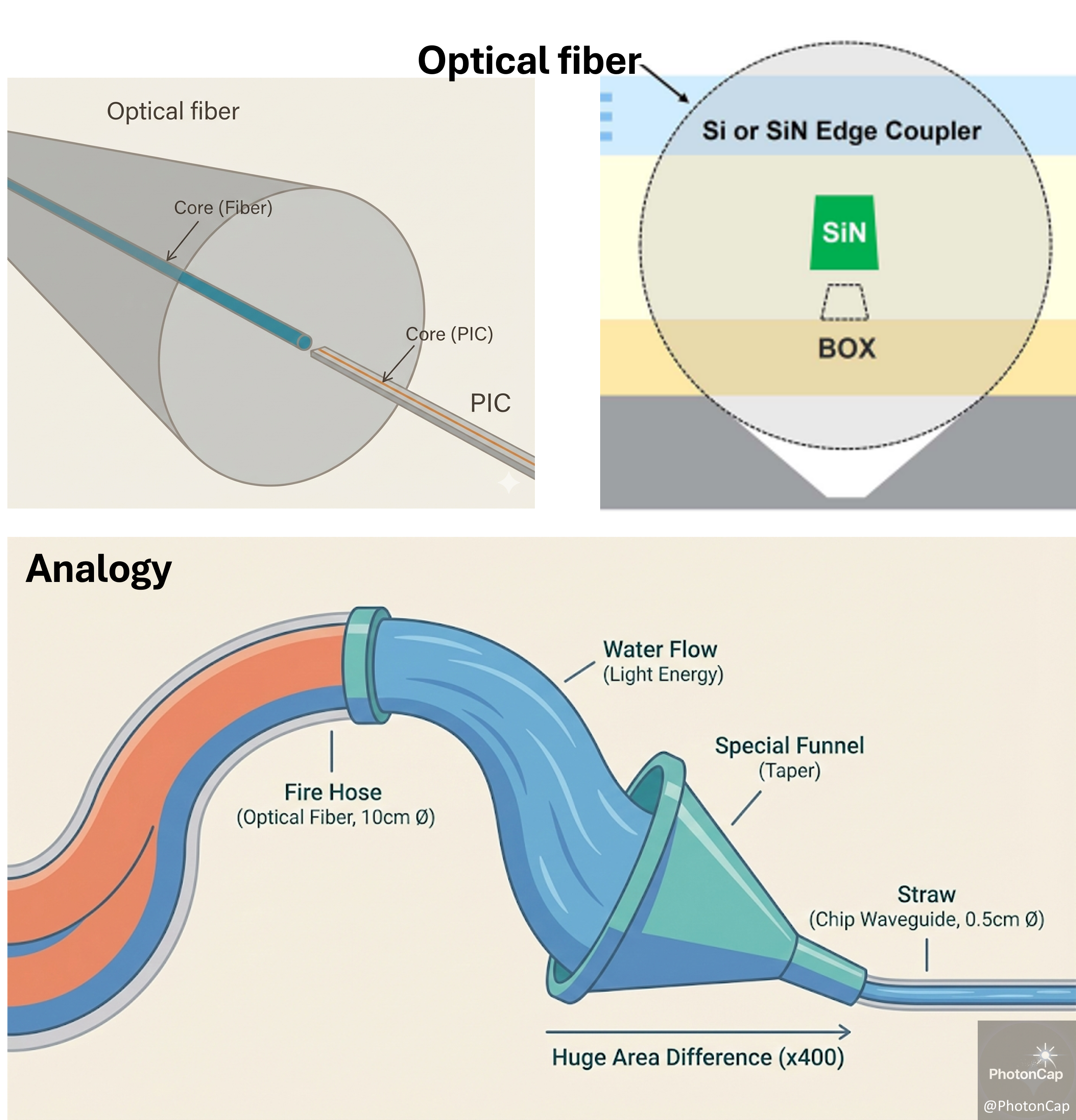
This is the gateway that forces the light from the massive Optical Fiber outside the chip into the tiny paths inside the chip. It also acts as a necessary ‘bridge’ when connecting chip to chip. In fact, while an optical fiber itself is very small (hair-thickness), compared to the light in the waveguide of a much smaller PIC chip, the optical fiber is truly massive.
💡 [Analogy: Plugging a Firehose into a Straw]
You have to put a stream of water from a 10cm diameter firehose (Fiber) pouring out at full force into a 0.5cm diameter tiny straw (Chip Waveguide) without spilling a single drop. It’s not just a 20x difference in diameter. If you calculate by the ‘area’ water passes through, the difference is far more massive. The cross-sectional area of the firehose is 400 times larger than the straw. In other words, you are trying to cram the massive water energy filling the hose cross-section into a hole 400 times smaller all at once. If you just put them together, water would splash everywhere, right? That’s why a ‘Special Funnel (Taper)’ that is as wide as the firehose at the entrance and narrows to the size of the straw at the end is absolutely necessary.
Couplers are also the core of passive devices. This is Optical I/O, the heart of packaging—one of the biggest bottlenecks in Silicon Photonics. We will discuss this in detail in Chapter 4, but for this Chapter, we will only summarize simple concepts.
2.1. Light is a Wave
Electrons struggle to cross a broken wire. However, light is both a particle and a wave. Therefore, it can cross to a certain level even if structures are not connected, and free-space communication is also possible.
To exchange light between a fiber and a chip, the beam size must be matched.
Sub-wavelength structures: Even if structures smaller than the wavelength of light are separated, light can jump between them.
Because of this, light signals can be transmitted across physically unconnected spaces through various light structures such as Edge couplers and Grating couplers.
Grating Coupler (Vertical): Allows for shooting light directly onto the wafer surface for testing without a dicing process, making mass production/testing/measurement speed overwhelming. However, narrow bandwidth and the loss of more than half the light leaking out are disadvantages.
Edge Coupler (Horizontal/SSC): Places the optical fiber right up against the side of the chip. Loss is negligible and performance is excellent, but packaging is extremely difficult and expensive. (This is the packaging direction high-performance AI chips like NVIDIA and Broadcom are aiming for.)
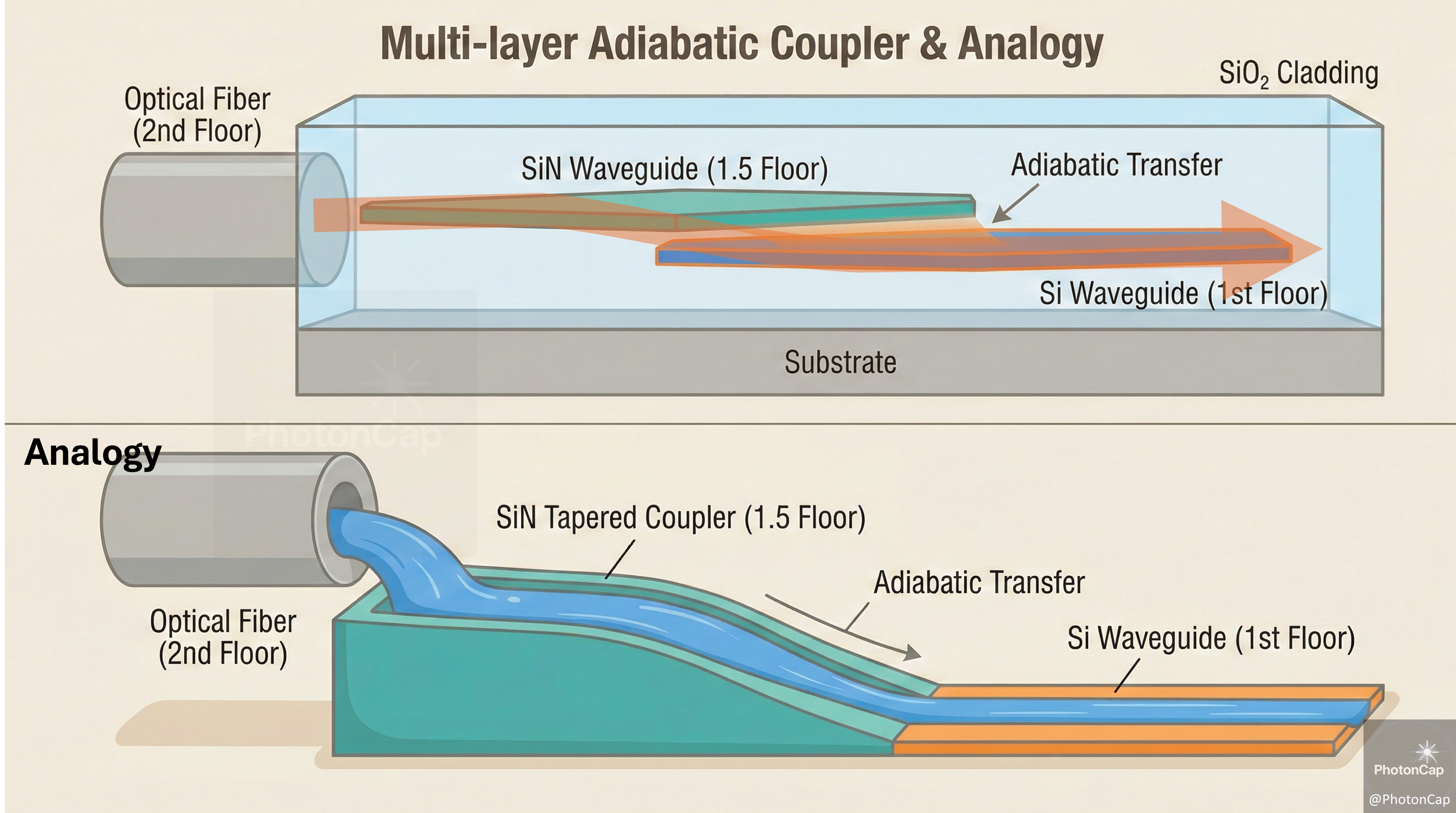
2.2. Evanescent Coupling
What GF (GlobalFoundries) / TSMC are attempting: SiN Stepping Stones
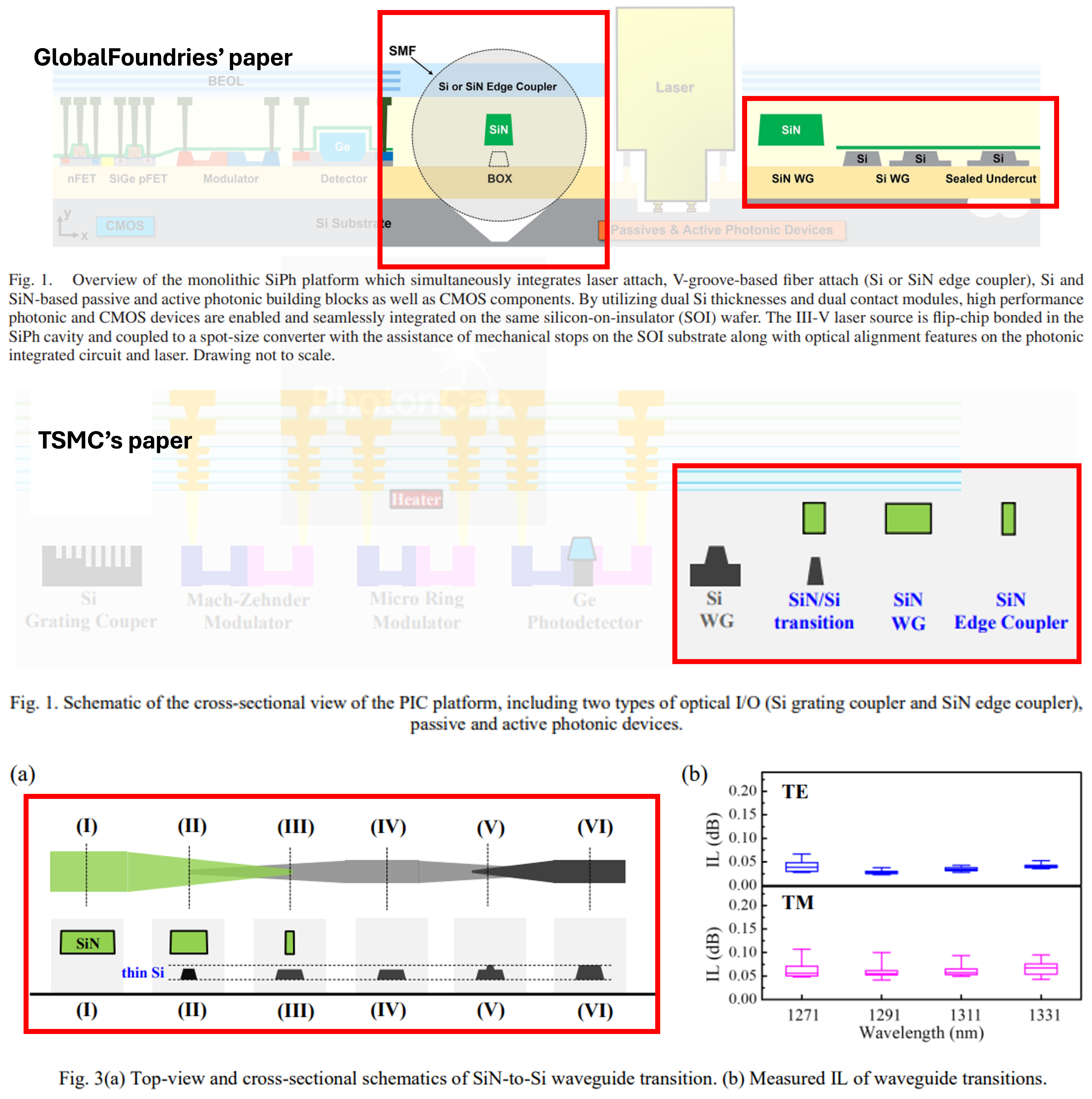
Recent foundries (GF Fotonix (top), TSMC (bottom), etc.) stack an intermediate layer called SiN (Nitride). By placing stepping stones in the order of [Optical Fiber (Large)] → [SiN Layer (Medium)] → [Silicon Layer (Small)], the light slides down smoothly without being startled. The foundry that implements this well with low loss wins the packaging war.
💡 [Analogy: Taking the Slide]
If you drop water directly from the 2nd floor (Fiber) to the 1st floor (Silicon), it all splashes. If you place a 1.5-floor platform (SiN) in the middle and connect them with a gentle slide (Adiabatic Taper), you can send the water down smoothly without spilling a drop.
2.3. PWB (Photonic Wire Bonding)
There is an innovative technology that has recently emerged outside of Silicon Photonics. It solves the complaint that “aligning optical fibers to chips is too hard (Align issue).”
Concept: Creating bridges of light with a 3D printer. Even if the chip and optical fiber are slightly crooked, it connects them with a Polymer material.
Advantage: Eliminates the need for precise alignment, drastically lowering packaging speed and cost.
Key Players: Germany’s Vanguard Automation, and Korea’s Lessengers — collaborating with POET — are standing out in this field.
First proposed by Prof. Koos’s team at KIT in Germany in 2012 (Optics Express), this technology is now being commercialized through Vanguard Automation and becoming a game changer in packaging.
3. Splitters, Resonators: Confluence Roads and Traffic Lights
These are the most basic building blocks that split, merge, and filter light.
Y-branch, MMI & DC: Devices that split light 1:2 or merge it.
Y-branch is intuitive.
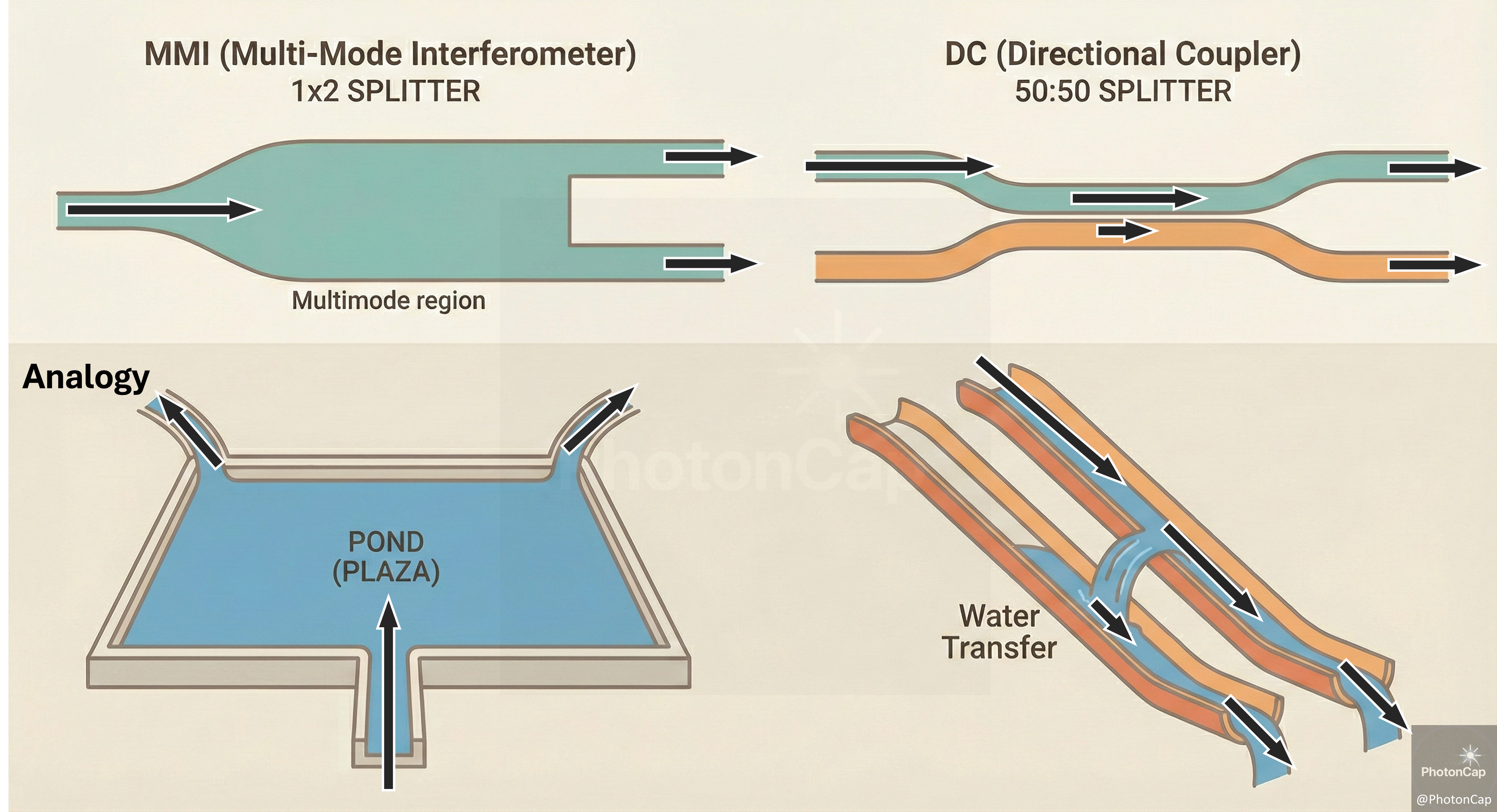
MMI (Multi-Mode Interferometer) is much more robust against process errors than a simple Y-shape, so it is preferred in actual mass-production chips. However, it has the constraint that it is difficult to perfectly support a wide bandwidth in the wavelength domain.
DC (Directional Coupler) is a tool that slowly transfers light from one arm to the opposite arm. Here, the two roads for light are separated by a very small distance. Through the wave nature of light, it is slowly transferred from one road to the other. Depending on the coupling length, the ratio can be changed to various values like 50:50, 0:100 (or 100:0), etc.
💡 [Analogy: Puddle Plaza (MMI)]
Digging a narrow Y-junction is difficult. Instead, we make a small square puddle (Plaza) in the middle. We let the water enter the puddle, slosh around for a bit, and then naturally overflow into two exits. Even if the canal is dug slightly crookedly, the water divides itself well.
MZI (Mach-Zehnder Interferometer): An advanced version of the DC. As a passive device, the MZI is a filter that passes only specific wavelengths. It uses the ‘minute time difference’ or ‘phase difference’ created when splitting light into two paths and recombining them to change the properties of the light. This is the core principle of the Modulator. (This will be covered in a later Modulator chapter.)
[Bridge to Active] When Passive Devices Meet Heat: What happens if you lay a metal Heater on one arm of an MZI? If you apply heat to change the refractive index, you can change the path of light from left to right in real-time. This is the principle of the Optical Switch.
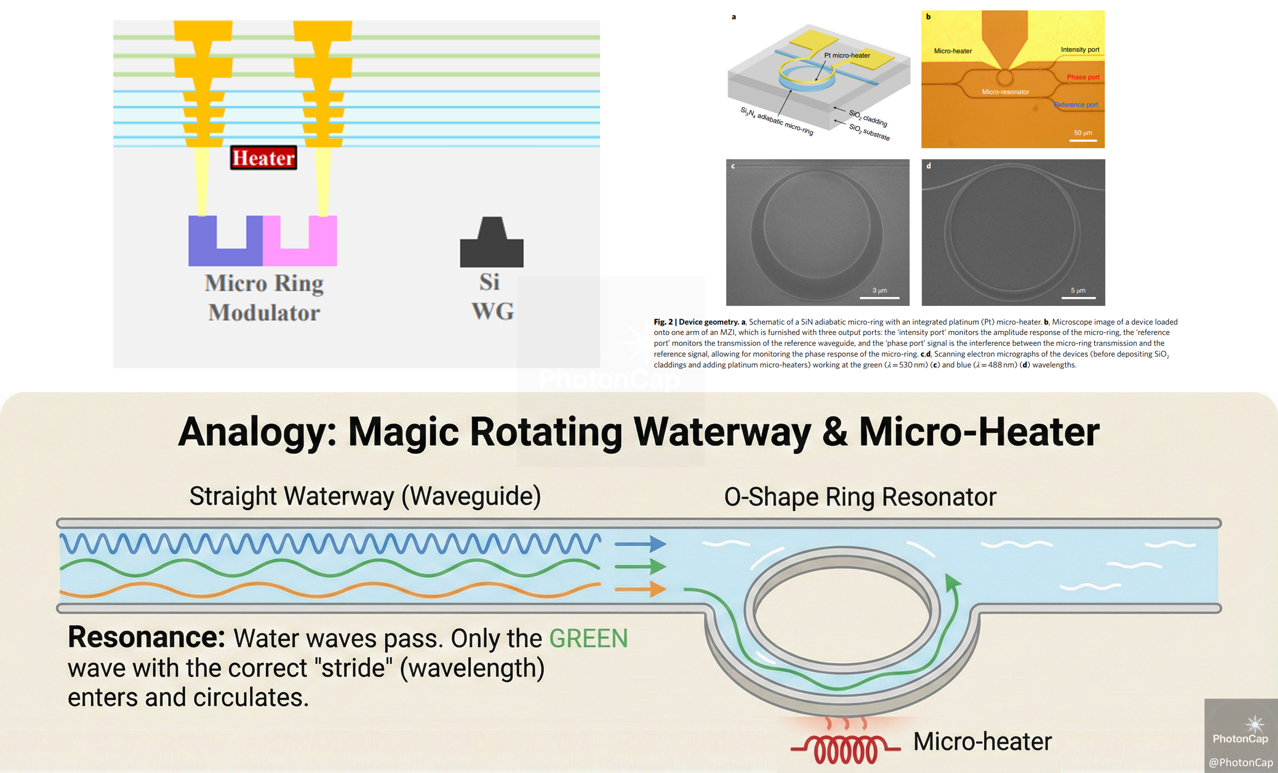
Ring Resonator: A small waveguide in the shape of a ring. It makes light of a specific wavelength spin around and around to trap or filter it.
Resonance Condition: 2πRn_eff = mλ. Resonance occurs only when the optical path length—the physical circumference (2π*R) multiplied by the effective index (n_eff )—is an integer multiple (m) of the wavelength (λ).
Although the structure itself is a passive device requiring no electricity, it is extremely sensitive to temperature changes, so an auxiliary device called a ‘Heater’ always follows it.
Silicon’s refractive index changes with temperature. Just someone blowing hot breath nearby can shift the wavelength the ring responds to.
This is a device that most Interconnect companies like Nvidia/Lightmatter/Ayar Labs/Xscape Photonics focus on.
💡 [Analogy: The Magic Roundabout and Floor Heating]
Resonance: Ripples flow past a straight canal. Usually, they just pass by, but ripples with a ‘specific stride length (wavelength)’ get sucked into the roundabout entrance and spin around. (This is magic that only happens when the ripple’s stride and the roundabout’s circumference match exactly.)
Sensitivity: The problem is the weather (temperature). When it gets cold, the dirt floor contracts, and the circumference of the roundabout shrinks slightly. Then, the ‘stride’ from before no longer fits, and the ripples cannot enter.
Heater: That’s why we install a boiler (Micro-heater) under the roundabout floor. Whether the weather is cold or hot, we maintain a constant floor temperature, or intentionally heat it up to slightly expand or shrink the circumference of the water channel, picking out only the ripples we want.
[Big Tech Move] TSMC’s COUPE (Compact Universal Photonic Engine) This is the platform name TSMC put forward recently (2024-2025) as it declared its full-scale entry into the Silicon Photonics market. The core is ‘3D Stacking’. It is a technology that stacks an electronic chip (EIC) vertically right on top of a chip with passive devices (waveguides, rings). The strategy is to compensate for the thermal/control weaknesses of ring resonators with TSMC’s packaging capabilities.
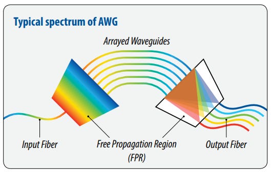
AWG (Arrayed Waveguide Grating): Spreads light of various wavelengths like a prism to separate or combine them. It is the key weapon Intel uses to implement Multi-wavelength (WDM) technology in data center chips.

Bragg Grating: Creates washboard-like irregularities inside the waveguide. It is a mirror and filter that reflects or passes only specific wavelengths.
4. Polarization and Crossing: The Shape of Light and Intersections
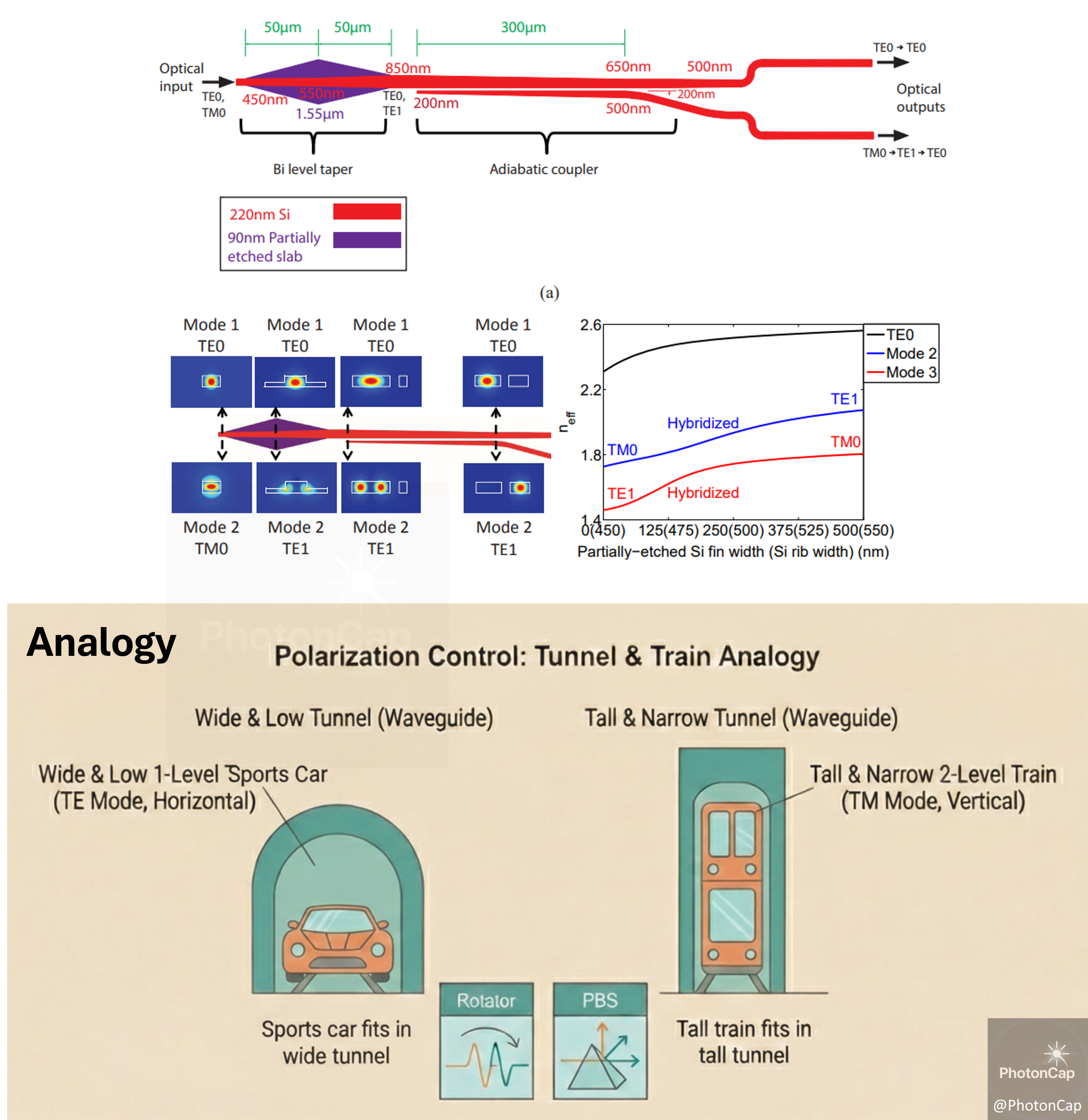
Polarization Control: Light has a direction in which it oscillates (Polarization). Usually called TE mode and TM mode, simply put, it’s the difference between oscillating vertically or horizontally. If this direction gets twisted while traveling, the signal dies inside the chip. (If the chip design is optimized for a specific polarization, it cannot support the other.) PBS (Polarization Beam Splitter) and Rotator are placed where needed in the chip to correct this.
💡 [Analogy: Tunnels and Vehicles]
It’s easy to understand if you compare the Polarization of light to the relationship between vehicles on a road and tunnels.
TE Mode (Flat Sports Car): Fits perfectly in a tunnel that is wide horizontally and low. Represents light that spreads wide left-to-right; optimized to pass through waveguides with low height.
TM Mode (Tall Double-Decker Bus): Fits perfectly in a tunnel that is narrow vertically and high. Represents light standing tall up-and-down; advantageous when passing through waveguides that are narrow and have high ceilings.
Core Control Elements:
Rotator: A device that turns a sports car on its side or lays a bus down flat. In other words, it physically twists the angle of the vehicle to match the tunnel shape.
PBS (Polarization Beam Splitter): Like a checkpoint at the tunnel entrance that designates “Low sports cars only!” or “Tall buses only!” and sorts out only the matching vehicles.
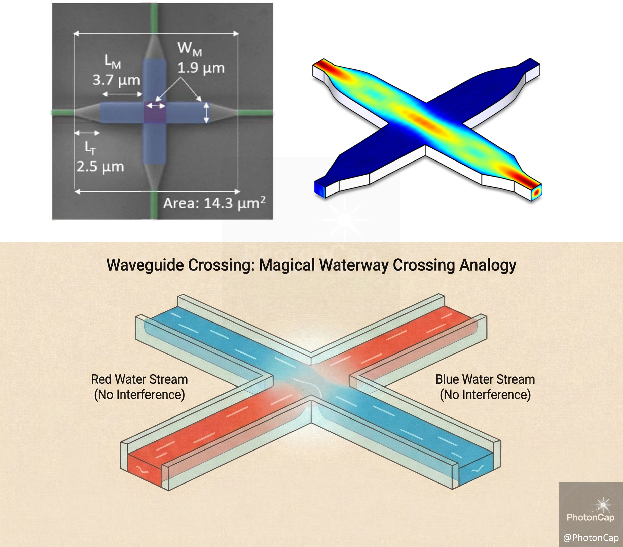
Waveguide Crossing: A 3D intersection design technology that allows paths of light to cross without interference. This technology must be good to use chip area efficiently.
💡 [Analogy: Grade-Separated Interchange]
Two water channels meet in a cross (+). In a normal channel, the water would mix here, creating whirlpools and chaos. But a light crossing is like a magical grade-separated interchange. Water flowing horizontally and water flowing vertically ignore each other’s existence and pass through like ghosts.
Actually, since light does not exchange mass or charge, it has the property of going its own way without interfering with each other even if passing through the same space. However, to ensure water doesn’t leak into the side roads in the middle of the intersection (Crosstalk), the core design know-how is precisely designing the entrance and exit so the water stream doesn’t scatter and shoots straight into the opposite channel.
5. PhotonCap’s Insight
Ultimately, passive devices are the ‘infrastructure’ that determines the efficiency of light, and the 0.1dB of loss saved here becomes the true Economic Moat that decides millions of dollars in electricity bills for data centers.
Moat of the PDK (Process Design Kit): Even with blueprints, if the passive device library matching the foundry’s characteristics is poor, the chip won’t work. Saying “We possess a verified passive device PDK” is the barrier to entry for a company.
1dB of loss is millions of dollars in power costs (OPEX): If you lose light in passive devices (Waveguide, Coupler, etc.) (Loss), you have to increase the output of the Laser Source or use unnecessary amplification (EDFA). In this case, heat generation inevitably increases. The greatest enemy of AI data centers is ‘Heat’. The technology to reduce passive device loss by 1dB or 0.1dB is the key to saving hyperscalers (customers) electricity bills.
Technology determining Packaging Costs (CAPEX): More than 50% of the price of a Silicon Photonics chip comes from packaging (assembly). If you have to attach optical fibers to chips one by one with expensive precision equipment (Active Alignment), mass production at a low cost is impossible.
Area Efficiency (Footprint): Reducing the size of passive devices is increasing the number of chips produced from a single wafer. This is directly linked to cost competitiveness.

Next Battlefield: Beyond Silicon to Glass (Glass Substrate/Waveguide):
Why are Intel, Corning, Samsung Electro-Mechanics, and Absolics Inc. (SKC) concentrating on ‘Glass Substrates’ recently? It’s not simply because they are hard. Glass is a ‘Top-tier Waveguide Material’ with extremely low propagation loss because the surface is much smoother than silicon, and at the same time, coupling loss with glass optical fibers is low.
The narrow alleyways inside the chip are handled by high-integration ‘Silicon Waveguides’, but the outer highways connecting chip to chip are handled by low-loss ‘Glass Waveguides’. In other words, the realm of passive devices is expanding from inside the chip to the external packaging area.
[Key Company]
Corning (GLW), Samsung Electro-Mechanics, Absolics (subsidiary of SKC)
For a detailed explanation of Glass Substrates, please refer to the article below.

6. References
Chrostowski, L., & Hochberg, M. (2015). Silicon Photonics Design. Cambridge University Press. (Chapters 3, 4)
Waveguide (IBM): Yurii A. Vlasov and Sharee J. McNab, “Losses in single-mode silicon-on-insulator strip waveguides and bends,” Opt. Express 12, 1622-1631 (2004)
Bend: Lichao Zhang, Jiamin Chen, Weichao Ma, Guangyuan Chen, Ruoming Li, Wangzhe Li, Junming An, Jiashun Zhang, Yue Wang, Guangyang Gou, Chunxiu Liu, Zhimei Qi, and Ning Xue, “Low-loss, ultracompact n-adjustable waveguide bends for photonic integrated circuits,” Opt. Express 31, 2792-2806 (2023)
Delay line: Hong, S., Zhang, L., Wu, J. et al. Multimode-enabled silicon photonic delay lines: break the delay-density limit. Light Sci Appl 14, 145 (2025)
SiN-Si (GFS): Y. Bian et al., “3D Integrated Laser Attach Technology on a 300-mm Monolithic CMOS Silicon Photonics Platform,” in IEEE Journal of Selected Topics in Quantum Electronics, vol. 29, no. 3: Photon. Elec. Co-Inte. and Adv. Trans. Print., pp. 1-19, May-June 2023,
SiN-Si (TSMC): H. Lu, C. Tang, C. Chen, B. Tan, W. Liu, H. Chiang, S. Tsai, T. Hsieh, W. Mao, W. Lo, S. Su, Y. Chen, H. Hsu, F. Tsui, E. Chen, C. Chu, V. Shih, and S. Huang, “Low-loss High-uniformity Silicon Nitride Optical Building Blocks Integrated on Silicon Photonics Platform,” in Optical Fiber Communication Conference (OFC) 2025, Technical Digest Series (Optica Publishing Group, 2025), paper Th1G.2.
Ring resonator: Liang, G., Huang, H., Mohanty, A. et al. Robust, efficient, micrometre-scale phase modulators at visible wavelengths. Nat. Photon. 15, 908–913 (2021).
AWG (SENKO): https://www.senko.com/wp-content/uploads/2021/09/Arrayed-Waveguide-Grating.pdf
Polarization: Wesley D. Sacher, Tymon Barwicz, Benjamin J. F. Taylor, and Joyce K. S. Poon, “Polarization rotator-splitters in standard active silicon photonics platforms,” Opt. Express 22, 3777-3786 (2014)
Crossing: Mack Johnson, Mark G. Thompson, and Döndü Sahin, “Low-loss, low-crosstalk waveguide crossing for scalable integrated silicon photonics applications,” Opt. Express 28, 12498-12507 (2020)
Crossing: https://optics.ansys.com/hc/en-us/articles/360042800433-Waveguide-crossing
Packaging: Weninger, D., Serna, S., Ranno, L. et al. Advances in waveguide to waveguide couplers for 3D integrated photonic packaging. Light Sci Appl 15, 17 (2026).
Glass substrate (Intel): https://www.intc.com/news-events/press-releases/detail/1647/intel-unveils-industry-leading-glass-substrates-to-meet
Glass substrate (Corning): Brusberg, Lars, et al. “Glass substrate for co-packaged optics.” IMAPSource Proceedings 2022.1 (2023): 000236-000241.
Great article! Thank you.