
[PC101] Lecture 2: Standing on the Shoulders of Giants — CMOS Process Leverage and Economic Moat

“If I have seen further it is by standing on the shoulders of giants”
Hello, this is PhotonCap.
If Lecture 1 explored “Why” Silicon Photonics is necessary, today’s story is about “How“ to make it, and more importantly, how to make it “Cost-efficiently.” This is the moment where “Capital Efficiency,” the core investment thesis of Silicon Photonics, truly explodes.
Isaac Newton said, “If I have seen further it is by standing on the shoulders of giants.” Silicon Photonics did not start from scratch either. It stands on the shoulders of the giant known as the ‘CMOS Semiconductor Process,’ built by humanity over the last 50 years with trillions of dollars in investment. By riding on this legacy, it has been able to open the path to commercialization so rapidly.
Today, connecting textbook principles (Silicon Photonics Design, Lukas Chrostowski) with real-world industry dynamics, we will uncover how we draw paths of light on a canvas of silicon and why this creates a formidable economic moat.
1. Paving the Highway of Light: Conductor vs. Mode
Sending signals inside a semiconductor chip follows completely different rules for Electrons and Photons (Light).
The Freedom of Electrons: Electrons simply need a ‘Conductor.’ Whether it’s a household wire, a PCB board, or nanometer-scale metal interconnects inside a chip, electrons will flow as long as there is a continuous metal path, even if it has bends and curves, relatively speaking compared to light.
The Pickiness of Photons: However, light cannot pass through metal, and in empty space, it tends to spread out in all directions (diffraction). To send light to a desired location, a simple path is not enough; a ‘Stable Mode’ must be formed that allows light to maintain its wave form while passing through.
To confine these tricky ‘optical modes’ within a fingernail-sized chip and transport them without loss, we use specialized platform materials.
(1) The Start of the Standard: SOI (Silicon-On-Insulator)
This is the current standard for Silicon Photonics and the starting point for all designs. We use a special wafer consisting of “Silicon (Si) - Oxide (SiO2) - Silicon” instead of a standard wafer.
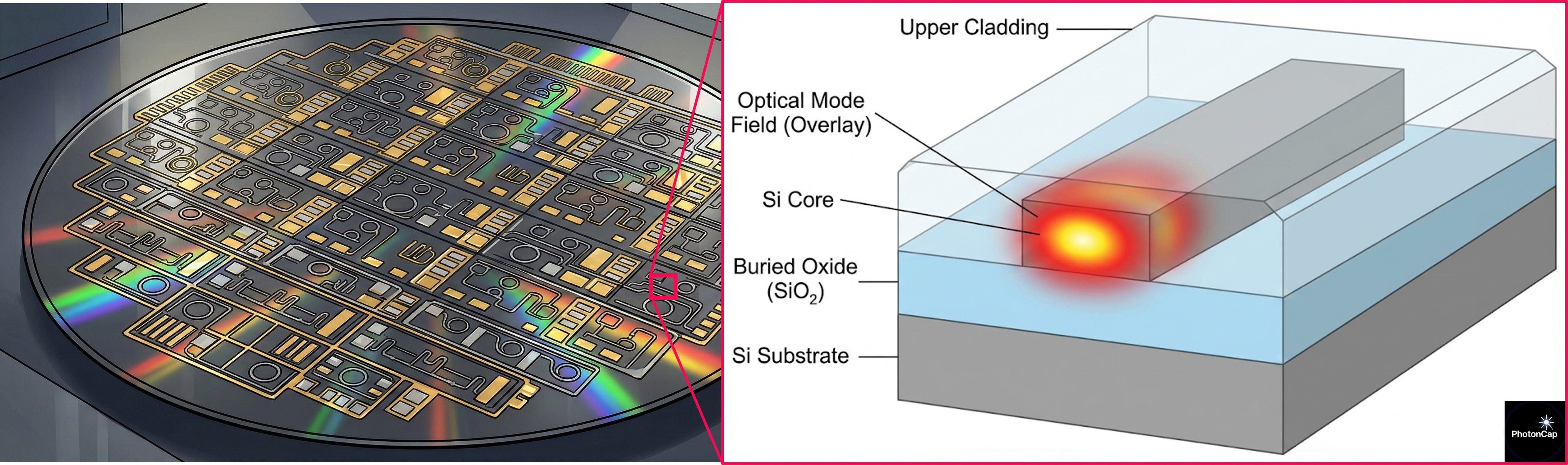
Overwhelming Refractive Index Difference (High Index Contrast): Traditional optical fibers have a refractive index difference of less than 1%, so their ability to confine light is weak. This necessitates a large volume. In contrast, SOI has a large difference between Silicon (~3.45) and Oxide (~1.44).
Extreme Miniaturization: Thanks to this powerful confinement, light does not bounce out even when bent at 90 degrees on a micrometer (µm) scale. This is the secret to shrinking a table-sized optical system onto a fingernail-sized chip.
(2) The New Trend: Silicon Nitride (SiN)
Recently, the Silicon Nitride (SiN) platform has emerged to complement the limitations of Silicon (Si). This is a material investors must know.
SiN is a common material originally used as an insulating film in semiconductor processes, but optically, it becomes an excellent ‘pathway for light’ that substitutes silicon. (Refractive Index ~2.0)
Low Loss: It has significantly lower light loss than silicon, making it advantageous for long-distance transmission or precise filter fabrication.
High Power Handling: Silicon has a fatal flaw where it absorbs light if the laser power is increased (Two-Photon Absorption), but SiN can withstand very strong lasers. Therefore, it is essential for chips used in Quantum Computing and LiDAR.
Thermal Stability: Unlike silicon, which is sensitive to temperature changes, SiN is insensitive to heat, making control easier.
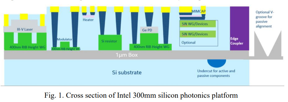
Hybrid Integration: Recently, Intel and GlobalFoundries have adopted a ‘Multi-layer’ process that stacks a Silicon (Si) layer and a Silicon Nitride (SiN) layer on a single chip like an apartment building, capturing the advantages of both materials.
(3) The Final Puzzle Pieces: InP and TFLN
There are things Silicon cannot do alone. For this, ‘mercenary materials’ are deployed.
Indium Phosphide (InP) - The Heart of Light: Silicon cannot emit light on its own. The prevailing technology involves directly attaching (Bonding) InP, which emits light when current flows, onto silicon to give the chip a heart.
Thin-Film Lithium Niobate (TFLN) - The King of Speed: A key material opening the 1.6T era. It possesses the property of instantly changing its refractive index when voltage is applied (Pockels Effect). Startups like HyperLight (platform) are leading the technology, and it is being adopted as a next-generation material by commercial module manufacturers.
(4) Others
BTO (Barium Titanate): It has a powerful weapon of being “CMOS Compatible.” Recently (Jan 2026), Veeco and imec secured mass production technology to directly deposit BTO on 300mm wafers, opening the way to create high-performance modulators without separate bonding.
EO Polymer: Theoretically the fastest. Lightwave Logic ($LWLG) successfully demonstrated single-channel 200Gbps (transmission speed) in 2024, proving the technical reality to open the 1.6T era. If thermal stability issues are perfectly resolved, it has a destructive potential in the pipeline.
Plasmonics: A technology that drastically reduces device size using metal nanostructures, being pioneered by Polariton Technologies.
2. The Nanometer Chisel: Lithography and Etching
Now that the canvas (SOI) is ready, we must draw the picture. This is where CMOS Process Leverage shines.
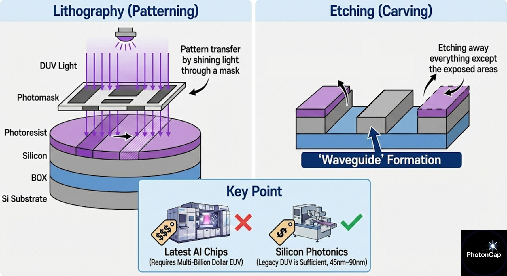
Drawing (Lithography): Patterns are transferred by shooting DUV (Deep Ultraviolet) light sources through a mask.
Carving (Etching): The areas hit by light are kept (or removed depending on resist type), and the rest is etched away to create a ‘Waveguide.’
💡 Wait a moment: Why does Silicon Photonics use ‘Legacy Equipment’? Semiconductor investors are usually enthusiastic about fine processes like 3nm or 5nm. However, Silicon Photonics is sufficient with DUV lithography using 193nm (ArF) or 248nm (KrF) wavelengths.
Wavelength vs. Node: DUV equipment shoots wavelengths in the 100nm~300nm band, but through technical correction, it can draw fine circuits (process nodes) at the 45nm~90nm level.
Mode Size: The ‘path of light (waveguide)’ we want to create inside the chip is usually around 400~500nm wide. Due to the physical size of the light wave itself, there is no need (and it is impossible) to shrink it to the 3nm level like a CPU.
Core: EUV equipment for the latest AI chips costs up to $350M per unit, and building an advanced fab equipped with them costs over $20B. In contrast, Silicon Photonics uses longer wavelengths of light, allowing the use of fully depreciated legacy DUV equipment to create world-class performance chips.
DUV: Deep Ultraviolet light, 100 nm - 300 nm wavelength. 248nm (KrF), 193nm (ArF)
3. [Textbook Insight] From Physics to Systems
Prof. Lukas Chrostowski defines the development stage of Silicon Photonics in his book as “A transition from Device-centric to System-centric.” Process technology alone is not enough. An ‘ecosystem to efficiently design and verify’ chips is needed.
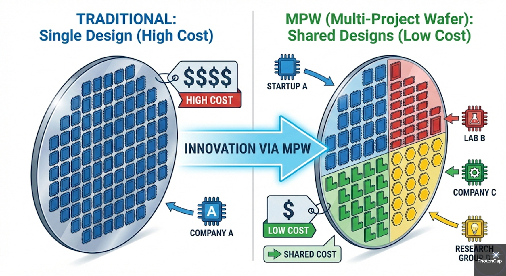
(1) MPW Service: The Catalyst of Innovation (A History of MPW)
In the past, to make a single chip, one had to buy an entire wafer, making the cost immense. However, the advent of MPW (Multi-Project Wafer) service started a revolution.
Concept: Like ‘Carpooling,’ it is a method where designs from multiple companies are loaded onto sections of a single wafer.
History: Organizations like ePIXfab in Europe, IME in Singapore, and OpSIS pioneered this ecosystem, and currently, imec, AIM Photonics, and others are continuing the legacy. Thanks to this, startups could verify prototypes at a low cost of tens of thousands of dollars, creating the soil for the current explosive fabless ecosystem.
(2) Electronic-Photonic Co-design
A point often overlooked is that a Photonic IC (PIC) alone can do nothing. To control light, collaboration with an Electrical IC (EIC) is essential.
Brain and Muscle (DSP & Analog): EIC is largely divided into two parts.
DSP (Digital): Acts as the ‘brain’ that mathematically calculates and removes signal noise. It is a 100% digital realm.
SerDes & Driver (Analog): Acts as the ‘muscle’ and ‘pathway’ that receives commands from the brain to actually transmit and receive light. This part is the pinnacle of ultra-high-speed analog technology.
Co-design: In the past, these were made separately, but now DSP (Digital) - SerDes (Analog) - PIC (Photonic Device) must be organically connected within a single package. This is why tools like Synopsys and Cadence, which enable this complex Heterogeneous design, are essential goods in the ecosystem.
[Deep Dive] The Final Gateway to Light (The Analog Gateway) “Silicon Photonics is a Light technology, so why is Analog electrical technology important?” Borrowing the insight of field expert (NuttyCLD), it is because data must run on an analog highway right until the moment it turns into light.
Highway Analogy: “The cargo (data) running on the highway and the control tower (DSP) are digital, but what paves that highway and withstands the physical speed is 100% analog technology.”
Investment Implication: Therefore, to break the bottleneck of AI data centers, both high-performance DSP IP (Marvell, Broadcom) and extreme Analog design capabilities (SerDes) are required. Companies that cover both these areas are the ones with true moats.
*Source:

4. [Simulation] Seeing Light in Advance: The Virtual Lab
“We designed it, but how do we know how the invisible light will move?” Baking a wafer takes months and hundreds of thousands of dollars. Therefore, ‘Multi-level Simulation’ that perfectly predicts the behavior of light in a computer before baking the chip is essential.
Lukas Chrostowski emphasizes in his book (Chapter 2) that “Silicon Photonics design is a process of integrating simulation tools of various levels.” Because fabrication is expensive and time-consuming, failing in advance within a computer is mandatory.
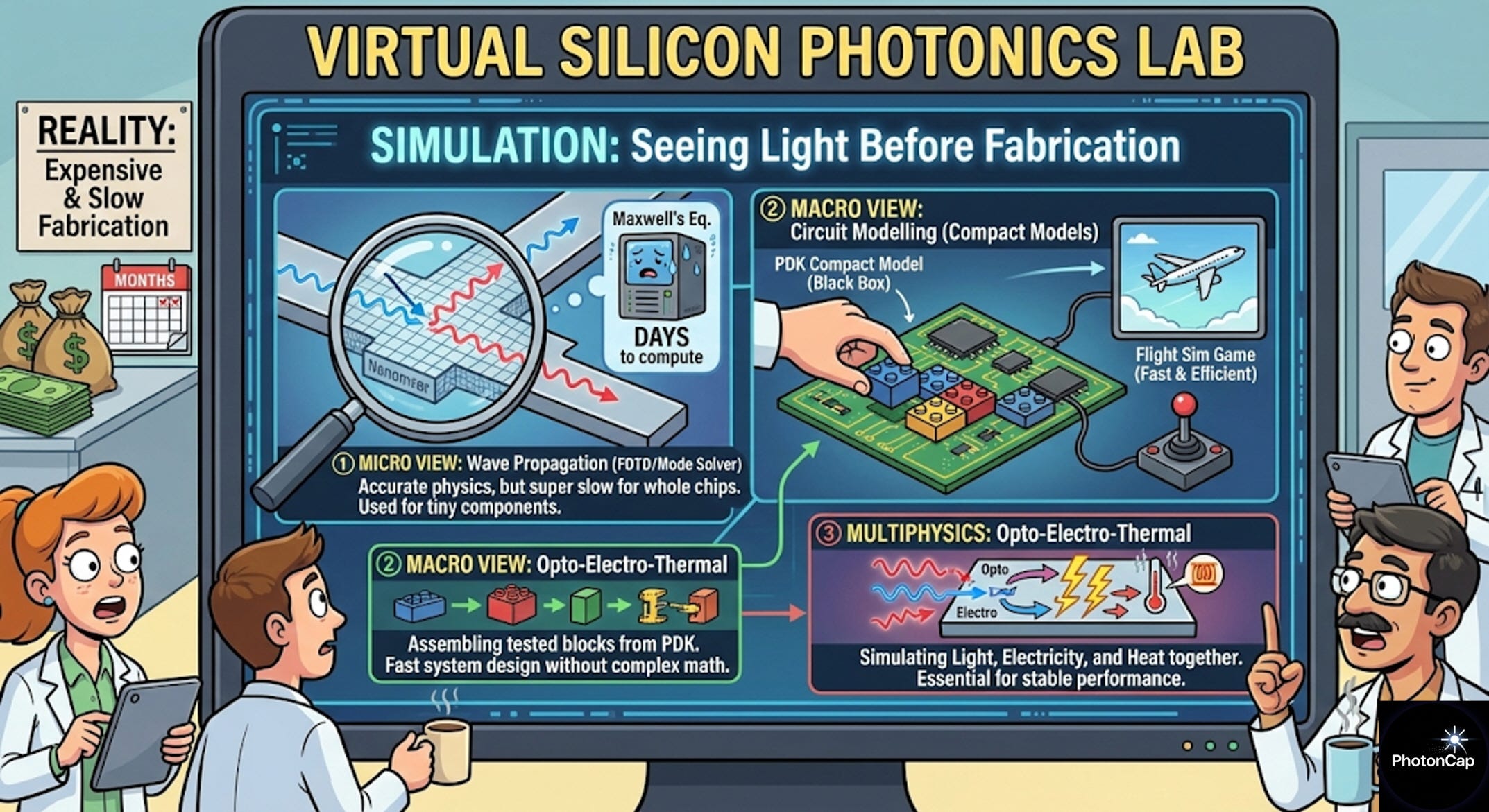
(1) Micro Perspective: Predicting Light Behavior (Wave Propagation)
The stage of calculating how light refracts and interferes within nanometer-scale structures.
Mode Solver: The most basic stage, checking what shape (Mode) light distributes into when confined in the cross-section of a waveguide.
FDTD (Finite-Difference Time-Domain):
Concept: A method of solving Maxwell’s Equations directly on a space-time Grid.
Characteristics: It shows the entire process of light refraction and scattering most accurately. However, the computational load is massive, so simulating an entire chip would take days even with a supercomputer. Thus, it is mainly used for designing very small core component units.
Efficient Alternatives (BPM, EME): Because FDTD is too slow, specialized algorithms are used according to the situation, such as BPM (Beam Propagation Method) which assumes light travels in only one direction, or EME (Eigenmode Expansion) which is advantageous for analyzing long structures.
(2) Macro Perspective: Assembling the Circuit (Photonic Circuit Modelling)
Running FDTD for a complex chip containing thousands of components would take years.
Circuit Simulation (Modelling): Speed and Efficiency.
Concept: FDTD cannot be used when designing the entire system. Instead, ‘Compact Models’ are used.
Analogy: It’s like using a supercomputer (FDTD) to analyze airplane wing aerodynamics, but using a lighter model (Circuit Model) for a flight simulation game.
Investment Point: PDKs (Process Design Kits) provided by foundries (TSMC, GF, etc.) contain already verified Compact Models. Designers can quickly design huge systems by assembling (Interconnect) these blocks without knowing complex formulas.
Compact Model: So, each component is simplified like a ‘black box’ to calculate only input and output values. It validates the performance of the entire system quickly, like assembling Lego blocks.
(3) Multiphysics: Light, Electricity, and Heat (Optoelectronic & Thermal)
Silicon Photonics does not deal only with light. Electricity and heat act in combination.
Electrical Modelling (Microwave Modelling): Simulates electrode design and impedance matching to process 100Gbps class high-speed signals.
Thermal Modelling: Silicon is very sensitive to temperature. A change of just 1 degree shifts the wavelength of light. Therefore, predicting the heat distribution inside the chip and designing a Heater to compensate for it is essential.
(4) Market Landscape: Tool Wars and EPDA
This complex simulation market has recently been reshuffled by large M&As.
Synopsys ($SNPS): Completed the acquisition of Ansys (the biggest fish in the industry) in 2025, becoming the strongest player holding both design (Synopsys) and physical analysis (Ansys/Lumerical). It sold its existing optical division (RSoft) to resolve antitrust issues.
Keysight ($KEYS): Entered the design market by acquiring Synopsys Optical Solutions Group (=Code V, RSoft, etc.). Adding ‘Simulation (Software)’ to existing ‘Measurement Equipment (Hardware),’ it has become a total solution company covering the entire Design-Verify-Test process. (The details of optical device testing will be covered in a separate [PC101] lecture, but the ‘importance of actual hardware verification’ is consistent with general semiconductors.)

Cadence ($CDNS): While competitors bought tools, it solidified its status as a ‘Design Platform (Virtuoso).’ No matter what simulator is used, the chip drawing (Layout) must eventually be drawn on Cadence.
FlexCompute (Tidy3D): A tool noticed by field engineers. It is a ‘Game Changer’ that finishes FDTD tasks, which used to take days, in minutes through cloud-based GPU acceleration.
COMSOL: The “Standard of Multiphysics.” It is still unique for solving complex problems where not only light but also heat (Thermal), stress (Stress), and electricity (Electrical) are intertwined.
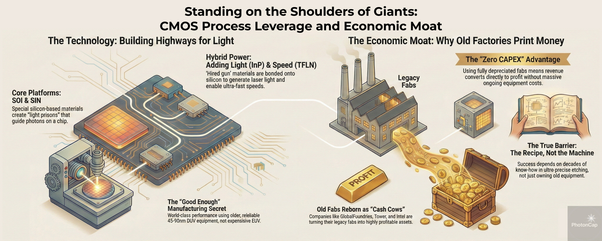
5. Economic Moat: Capital Efficiency
This is the powerful Economic Moat that Silicon Photonics possesses.
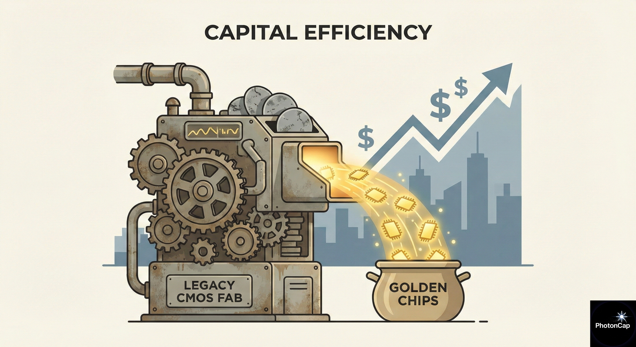
(1) Zero CAPEX Magic: A Fully Depreciated Cash Machine
Equipment costs (depreciation) account for 30~50% of semiconductor manufacturing costs.
Cost Advantage: While competitors pour 20 trillion KRW (approx. $20B) to build a single new 3nm process fab and write off trillions in depreciation costs annually, Silicon Photonics companies print chips with ‘Fully Depreciated’ equipment that achieved ROI 10 years ago.
Profitability: It is a structure where revenue leads directly to operating profit without the burden of fixed costs. This is why legacy foundries (GlobalFoundries, Tower) are betting their lives on Silicon Photonics.
(2) Golden Yield: 20 Years of Maturation
In semiconductors, ‘Yield’ is money.
Risk Free: The latest fine processes take astronomical money and time just to stabilize initial yield. However, the 45nm~90nm process is a technology humanity has perfectly mastered over the last 20 years by printing billions of wafers.
Stability: There are almost no process troubles (Defects), and when a wafer is inserted, golden good products pour out as expected. This is a huge attraction point for Data Center customers who prioritize supply chain stability.
(3) The ‘Looks Easy’ Trap: The Recipe is the Moat (The Technical Barrier)
The most common misunderstanding by investors is, “Since they use old equipment, won’t China catch up quickly?” However, this is not a problem of ‘Equipment’ but a problem of ‘Recipe.’
Sidewall Roughness: Electrons pass through well even if the circuit walls are a bit rough, but light scatters and the signal disappears if the wall is rough by even 1nm. Extreme Etching know-how is required to carve out surfaces smoother than the latest processes while using old equipment.
Heterogeneous Integration: Packaging technology that attaches lasers (InP) or combines heterogeneous materials on silicon is an area of ‘Tacit Knowledge’ accumulated over decades that cannot be solved simply by buying equipment. This is the true moat held by Intel and Tower Semiconductor.
6. [Real World] The Renaissance of Legacy Fabs
“I get that it’s efficient in theory, but does it actually make money?” Let’s check how old equipment keeps running without stopping, and how factories with finished depreciation are reborn as ‘Geese laying Golden Eggs.’
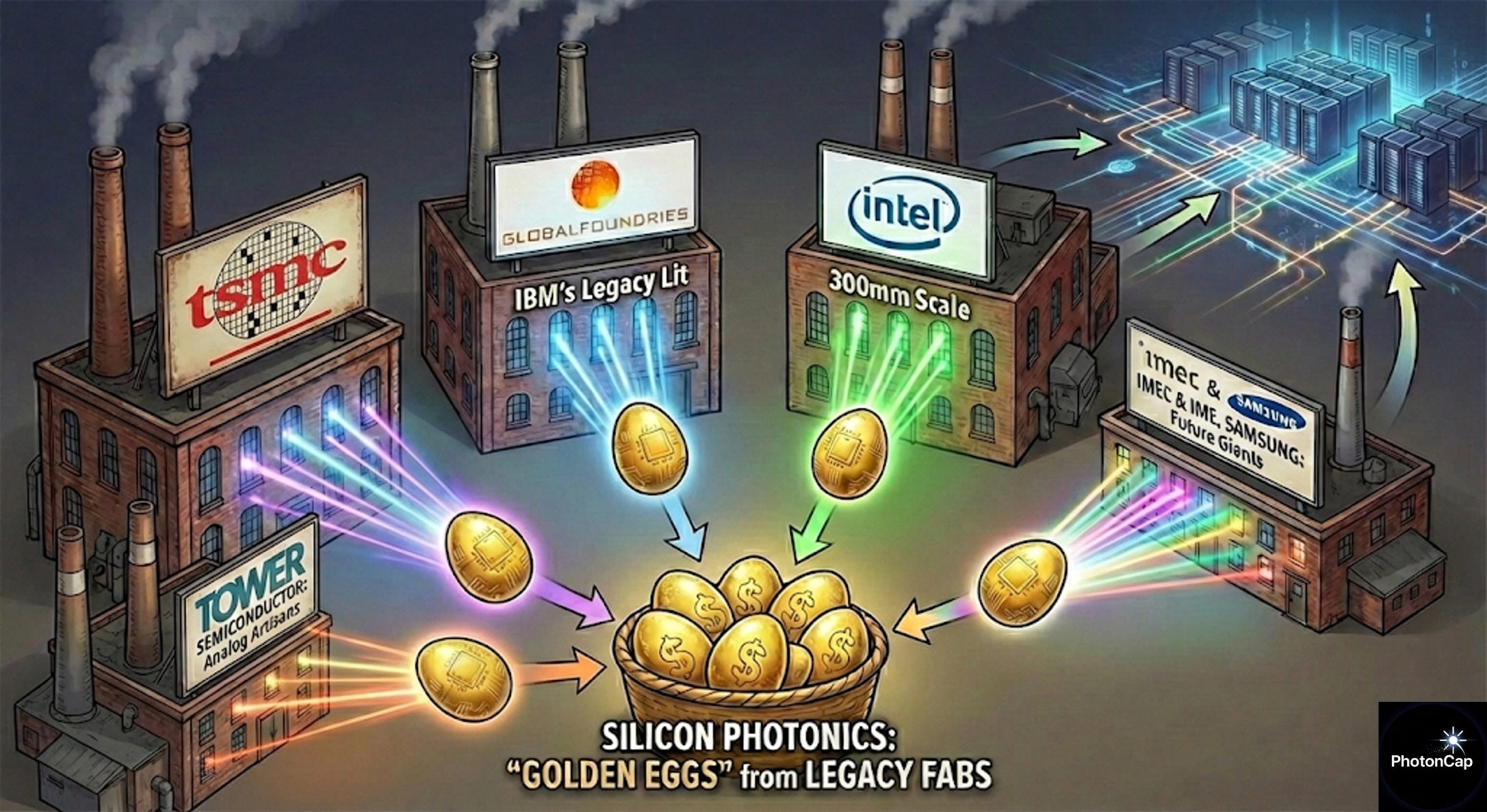
(1) TSMC ($TSM): Exquisite Harmony of 65nm and 3D Packaging
Location: Taiwan Hsinchu & Taichung (Advanced Backend Fab)
Strategy: Utilizing COUPE (Compact Universal Photonic Engine), it is the textbook example of ‘Hybrid.’ The electrical chip (EIC) controlling light uses the cheap, fully depreciated 65nm process, but when stacking it on the optical chip (PIC), it uses cutting-edge SoIC-X (Hybrid Bonding) technology. It shows the extreme of ‘Smart Capital Efficiency’ by maximizing performance with packaging while utilizing legacy equipment.
Performance: Aiming for mass production in 2026, it has secured massive clients like NVIDIA (Vera Rubin) and Broadcom. It reigns as a new predator in the CPO ecosystem as a ‘One-Stop Platform’ that reduces total system power consumption by over 70%.
(2) Tower Semiconductor ($TSEM): The Luxury Workshop of Analog Artisans
Location: USA California Newport Beach (Fab 3), Japan TPSCo, Italy Agrate
Strategy: This 200mm (8-inch) Fab built in 2002 was originally a place making wireless communication chips (RF). Tower combined its specialty SiGe (Silicon Germanium) technology here to complete a unique Silicon Photonics platform called ‘PH18.’ Tower also unveiled a 300mm Silicon Photonics process offering, expanding mass production options.
Performance: Collaborating with Innolight, chips for 400G/800G optical modules currently entering AI data centers are being mass-produced in this ‘old factory.’ It is a representative example showing the world’s best high-speed signal processing capability without the latest advanced processes.
(3) GlobalFoundries ($GFS): Turning IBM’s Legacy into Light
Location: USA New York Malta (Fab 8) & Singapore
Strategy: It acquired the legendary lines that used to print IBM CPUs and transformed them into a major Silicon Photonics foundry. In particular, the ‘90WG (90nm)’ and ‘45SPCLO (45nm)’ processes have become standard platforms most sought after by fabless companies worldwide. It is especially strengthening solutions that handle packaging in a turnkey manner in conjunction with the Singapore Fab.
Performance: Recently, through the ‘Monolithic Process’ that puts optical devices and electronic devices all into one chip, it overcomes the limits of legacy processes with technology and boasts an overwhelming market share.
(4) Intel ($INTC): Economies of Scale with 300mm Wafers
Location: USA New Mexico & Oregon Fabs
Strategy: Intel’s greatest strength is its ‘Hybrid Laser-on-wafer’ technology. While competitors used 200mm wafers, it achieved economies of scale by deploying 300mm fabs used for CPUs. Recently, by selling its transceiver division to Jabil ($JBL), Intel has shifted its strategy to focus on the inherent technology and reliability of the chip (PIC) itself.
Performance: While others were frantic about the 3nm fine process competition, Intel pushed manufacturing proficiency to the limit on its fully depreciated 300mm lines. As a result, it set a record of shipping over 8 million PICs and 32 million integrated lasers. Notably, in the reliability sector, the biggest challenge of Silicon Photonics, it recorded a Laser FIT (Failures In Time) of less than 0.1, a figure that overwhelmingly exceeds the reliability standards accepted in the industry.
(5) [Potential Game Changers] Research Institutes and Awakened Giants
Besides the traditional powerhouses, there are R&D hubs and a new giant that must be watched.
imec (Belgium) & IME (Singapore): Midwives of the Ecosystem
Role: They are not general companies seeking profit but ‘Top-tier Research Institutions’ formed by alliances of nations and companies. Even Intel or Samsung go here when they hit a wall.
Strategy: Before commercial fabs run, imec (iSiPP platform) and IME develop the most leading process recipes and set standards. They are the hidden heroes who nurtured the global fabless ecosystem by providing initial MPW services, especially to startups.
Samsung Electronics: The Counterattack of the Memory Empire
Movement: Although quieter than Intel in Silicon Photonics so far, it recently signaled its role as a packaging solution provider by submitting a related paper to the 2026 OFC (Optical Fiber Communication Conference).
Strategy (Advanced Packaging): Samsung’s weapon is not simple optical device manufacturing. It is the ‘Turn-key Packaging (I-Cube, X-Cube)’ capability combining Memory (HBM) and Foundry.
Outlook: Even if the optical device uses a legacy process, in the battle of ‘How to put it into one package (Co-packaging) with the latest AI accelerators and HBM,’ Samsung is the ‘Game Changer’ with the strongest potential.
7. PhotonCap’s Insight
“Who is mining gold with an old pickaxe?”
First, the ‘Legacy Fabs’ held by GlobalFoundries or Tower should be re-evaluated as the most efficient ‘Cash Cows’ in the Silicon Photonics era.
The power of software is also strong, not just hardware. Thanks to the complex difficulty of having to design (Co-design) electrons and photons simultaneously, Synopsys and Cadence, who monopolize this simulation environment, are the true winners collecting tolls in the ecosystem. Also, the moats of Soitec and Shin-Etsu, who hold the SOI wafers that are the starting point of all processes, remain solid.
Finally, the ‘absolute necessity’ we must pay attention to is Test and Measurement. Because no matter which foundry or platform wins, the manufactured chip must prove its performance. In particular, FormFactor ($FORM), the leader in wafer-level testing, and Keysight ($KEYS), the standard for measurement instruments, are the safest investment destinations that can generate profit regardless of the outcome of the platform competition. Among them, FormFactor’s CM300xi-SiPh is considered a unique equipment in the industry that automates nanometer-level optical alignment. This equipment is the core key that allowed Silicon Photonics to move beyond lab prototypes into the era of mass production based on 300mm wafers, and the technological reality that allowed FormFactor to monopolize the entrance to this market.
8. References
Chrostowski, L., & Hochberg, M. (2015). Silicon Photonics Design. Cambridge University Press. (Chapters 1.1, 1.2, 1.5)
🏭 Process & Foundry
TSMC:

TSMC & NVIDIA: https://developer.nvidia.com/blog/a-new-era-in-data-center-networking-with-nvidia-silicon-photonics-based-network-switching/
Tower: https://towersemi.com/technology/rf-and-hpa/silicon-photonics-rf/
Intel: https://www.intel.com/content/www/us/en/research/integrated-photonics.html
Intel: https://newsroom.intel.com/artificial-intelligence/intel-unveils-first-integrated-optical-io-chiplet
Intel: Li, Kejia, et al. “Intel 300mm Heterogeneously Integrated Silicon Photonics Technology: A Review of Recent Progress.” Optical Fiber Communication Conference. Optica Publishing Group, 2025.
Intel & Jabil: https://optics.org/news/14/11/3
GlobalFoundries: https://gf.com/blog/next-gen-gf-fotonix-redefining-flexibility-bandwidth-upgrades-full-turnkey-support/
imec IC-link (Si/SiN): https://www.imeciclink.com/en/asic-fabrication/si
🧪 Next-Gen Materials
imec & Veeco (BTO): https://www.imec-int.com/en/press/veeco-and-imec-develop-300mm-compatible-process-enable-integration-barium-titanate-silicon
Lightwave Logic (Polymer): https://www.prnewswire.com/news-releases/lightwave-logic-demonstrates-world-class-200gbps-heterogeneous-polymersilicon-photonic-modulator-results-302097749.html
💻 Design & EPDA
Cadence & Ansys: https://optics.ansys.com/hc/en-us/articles/4417886316819-Cadence-Interoperability-Overview
Synopsys & Ansys: https://investor.synopsys.com/news/news-details/2025/Synopsys-Completes-Acquisition-of-Ansys/default.aspx
🔬 Test & Measurement
FormFactor (CM300xi-SiPh): https://www.formfactor.com/product/probe-systems/300-mm-systems/cm300xi-siph/
🚀 Insights & Evidence
Samsung Electronics @OFC 2026:


UC Berkeley (Foundry Cost Analysis): https://www2.eecs.berkeley.edu/Pubs/TechRpts/2021/EECS-2021-205.pdf
Intel(R) Pentium(R) 4 Processor on 90 nm Process Datasheet: https://www.intel.com/content/dam/support/us/en/documents/processors/pentium4/sb/30056103.pdf
Texas Instrument Blog (45- to 130-nanometer): https://www.ti.com/about-ti/newsroom/company-blog/the-importance-of-ensuring-supply-for-foundational-semiconductor-chips.html
🔗 [PC101] Previous Lecture
[KOR]
제1강: 왜 지금 ‘실리콘 포토닉스’인가?
)
[ENG]
Lecture 1: Why ‘Silicon Photonics’ Now?
Great read. Recently did a deep dive on Ansys too. Very exciting company: https://manuelwalz.substack.com/p/synopsys-snps-vs-dassault-systemes?r=73hd6l