
[PC101] Lecture 1: Why 'Silicon Photonics' Now? (The Next Fabless Revolution)

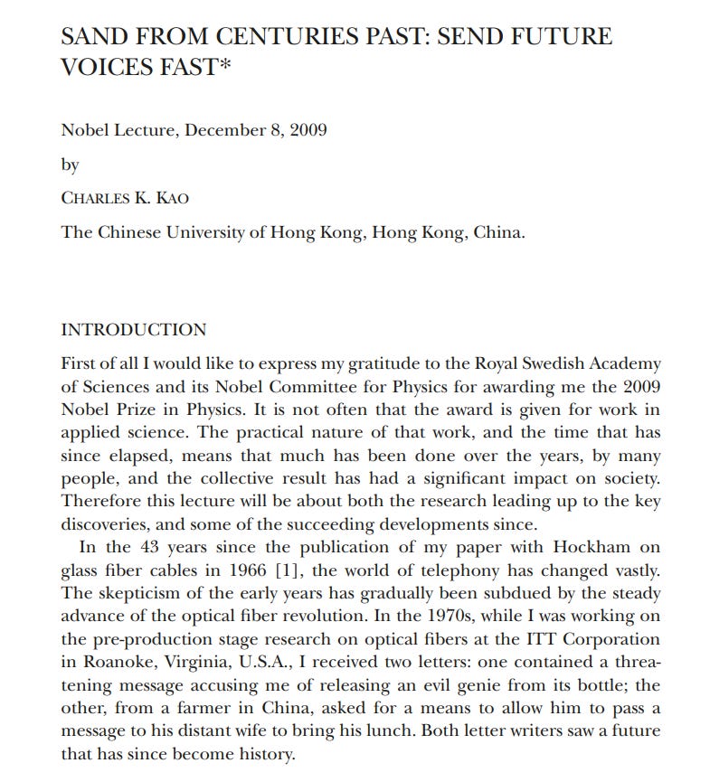
“Sand from Centuries Past: Send Future Voices Fast”
This was the title presented by Professor Charles K. Kao, the ‘Father of Fiber Optics,’ during his Nobel Prize acceptance lecture in 2009. His insight that ordinary ‘sand (glass)’—present for millennia—would become an information superhighway carrying light completely transformed humanity’s communication history. And now, in 2026, we stand at another monumental turning point: shifting that path of light beyond glass fibers onto silicon chips.
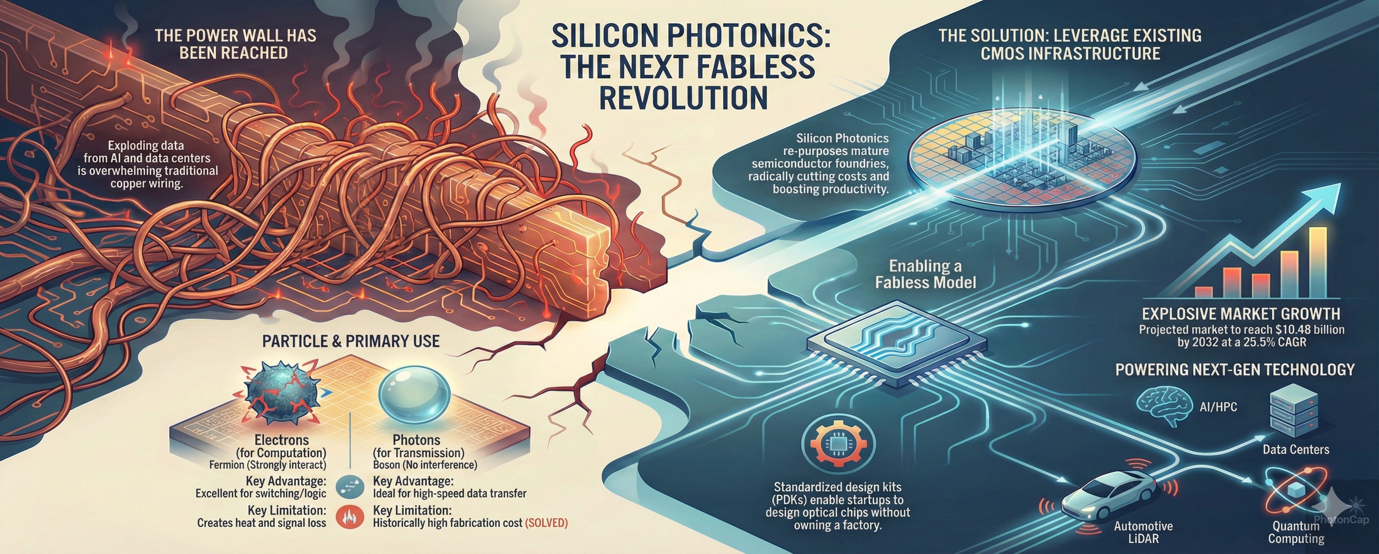
With the explosive growth of generative AI and data center traffic, existing ‘electron’-based semiconductors have hit the physical limit known as the ‘Power Wall’. Copper wires heat up and signals distort the faster data is sent.
The semiconductor industry is now experiencing a ‘Second Fabless Revolution’ comparable to the 1980s VLSI (Very Large Scale Integration) revolution. At the heart of this is the technology known as ‘Silicon Photonics’. In Lecture 1, we explore why this technology demands attention now, identifying the macro-level shifts and key players investors should watch.
1. The Scream of Copper Wires: The Limits of Electrons (The Power Wall)
The computing systems we use rely on ‘electrons’ traveling through copper wires to transmit information. However, as data transmission volumes have grown exponentially, this method has reached a critical point.
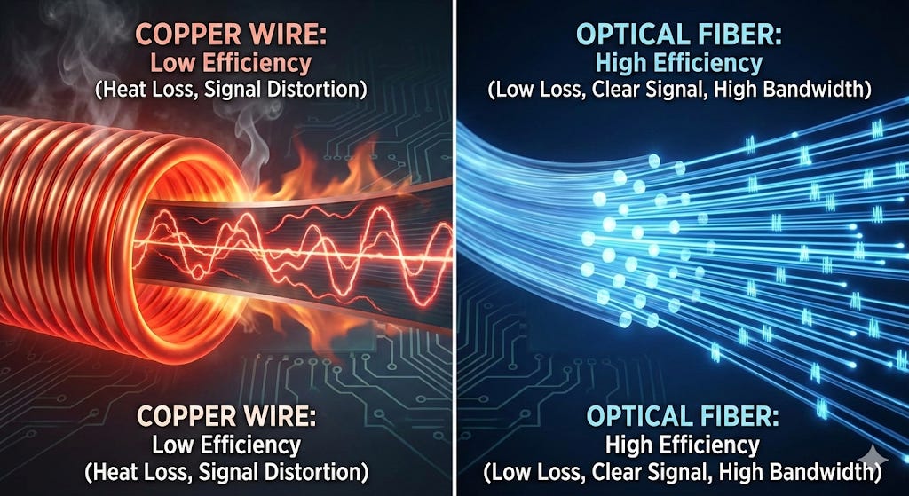
Bandwidth and Heat Bottlenecks: Electrons possess Fermion properties—they interfere with and repel each other—making them advantageous for computation (switching) but disadvantageous for transmission (interconnect). To transmit data at high speeds through copper wires requires massive amounts of power, which directly leads to signal attenuation and enormous heat generation. Currently, a significant portion of power in AI data centers is consumed not by computation, but by ‘data movement’ and cooling it.
The Rise of Photons: Conversely, photons—particles of light—possess the property of not interfering with each other (Bosons). This enables WDM (Wavelength Division Multiplexing), which carries multiple wavelengths (colors) of light simultaneously over a single channel, allowing much faster travel over much greater distances without energy loss.
The industry’s conclusion is now clear: the structural shift where “computing is handled by electrons, and transmission by light” is no longer a choice but a necessity for survival.
2. The Second Fabless Revolution: “Chips Made Without Being a Physicist”
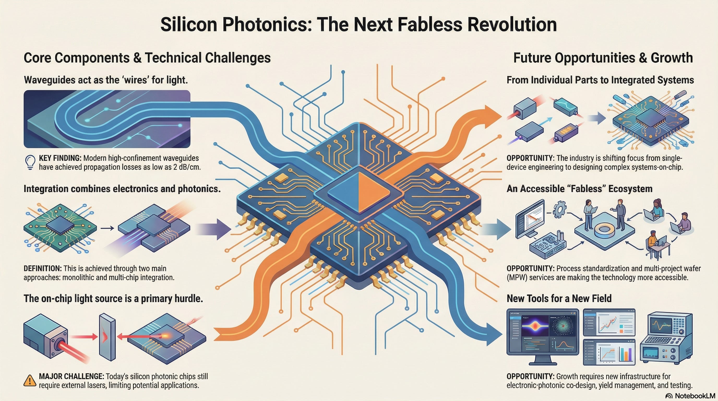
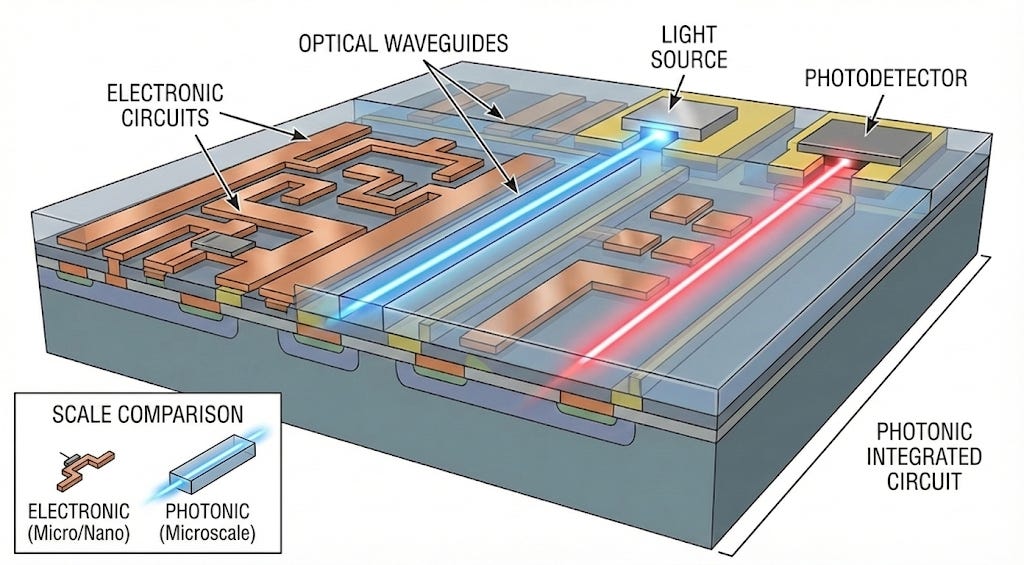
Design Paradigm Shift: “From Device Physics to System Architecture” While past optical design was the domain of ‘device physics’—grappling with nanometer-scale structures and solving Maxwell’s equations—silicon photonics has now entered a stage of high-level abstraction.
Information Hiding of Physical Complexity: The PDK (Process Design Kit) provided by foundries now goes beyond simple device libraries, integrating with verified compact models. Designers focus on system metrics like bandwidth, power consumption, and latency when designing ‘photonic fabrics,’ rather than grappling with the underlying complex physical phenomena.
The Completion of EPDA (Electronic-Photonic Design Automation): With the full integration of electronic semiconductor (EDA) tools and optical design tools, photonic semiconductor design is now part of a standardized engineering workflow, not specialized research.
The Era of System Architects: Just as NVIDIA once dominated the market by focusing on GPU architecture, this signals the dawn of an era where system design companies defining ‘how to solve computing bottlenecks using light’ take the lead, rather than firms excelling at making individual components.
3. Economic Moat: Standing on the Shoulders of Giants (Leveraging the CMOS Infrastructure)
From an investment perspective, silicon photonics’ strongest appeal is its ‘capital efficiency’.
Reusing CMOS Processes: Existing optical communication devices required dedicated factories for expensive III-V compound semiconductors like indium phosphide (InP). Silicon photonics, however, leverages the CMOS production lines already established and refined over decades by Intel, TSMC, and GlobalFoundries.
Rediscovering the Value of Legacy Processes: Light’s wavelength (1.31µm and 1.55µm for optical communications) is significantly larger than electrons. Therefore, there is no need for ultra-fine 3nm or 5nm processes costing billions of dollars. Even with depreciated legacy equipment at the 65nm to 130nm level, world-class optical chips can be mass-produced.
This represents a massive economic moat, enabling the avoidance of new fab construction costs while securing overwhelming yield and price competitiveness. In practice, Tower Semiconductor leverages Intel’s depreciated 65nm process (Fab 11X) to produce high-performance chips. This model of ‘recycling’ existing assets without billions of dollars in new CAPEX is the essence of silicon photonics’ cost competitiveness.
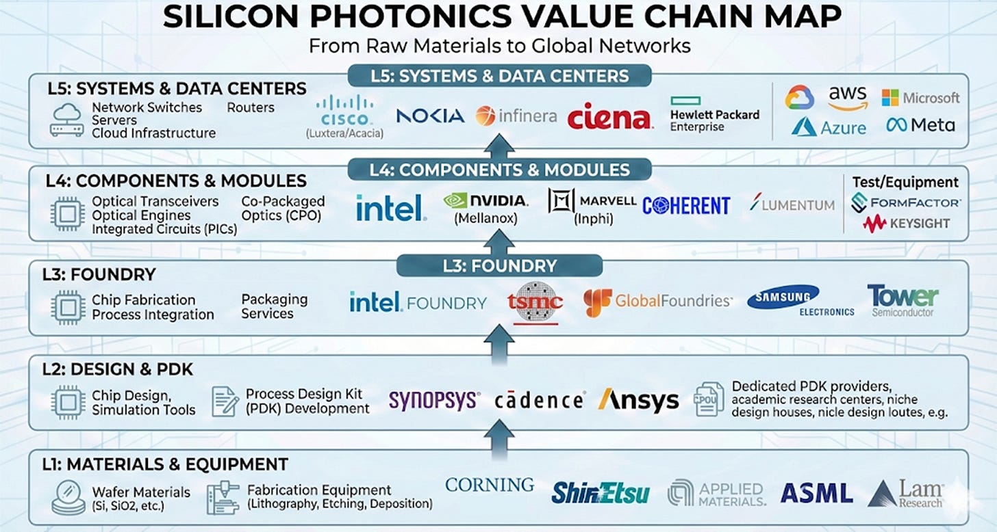
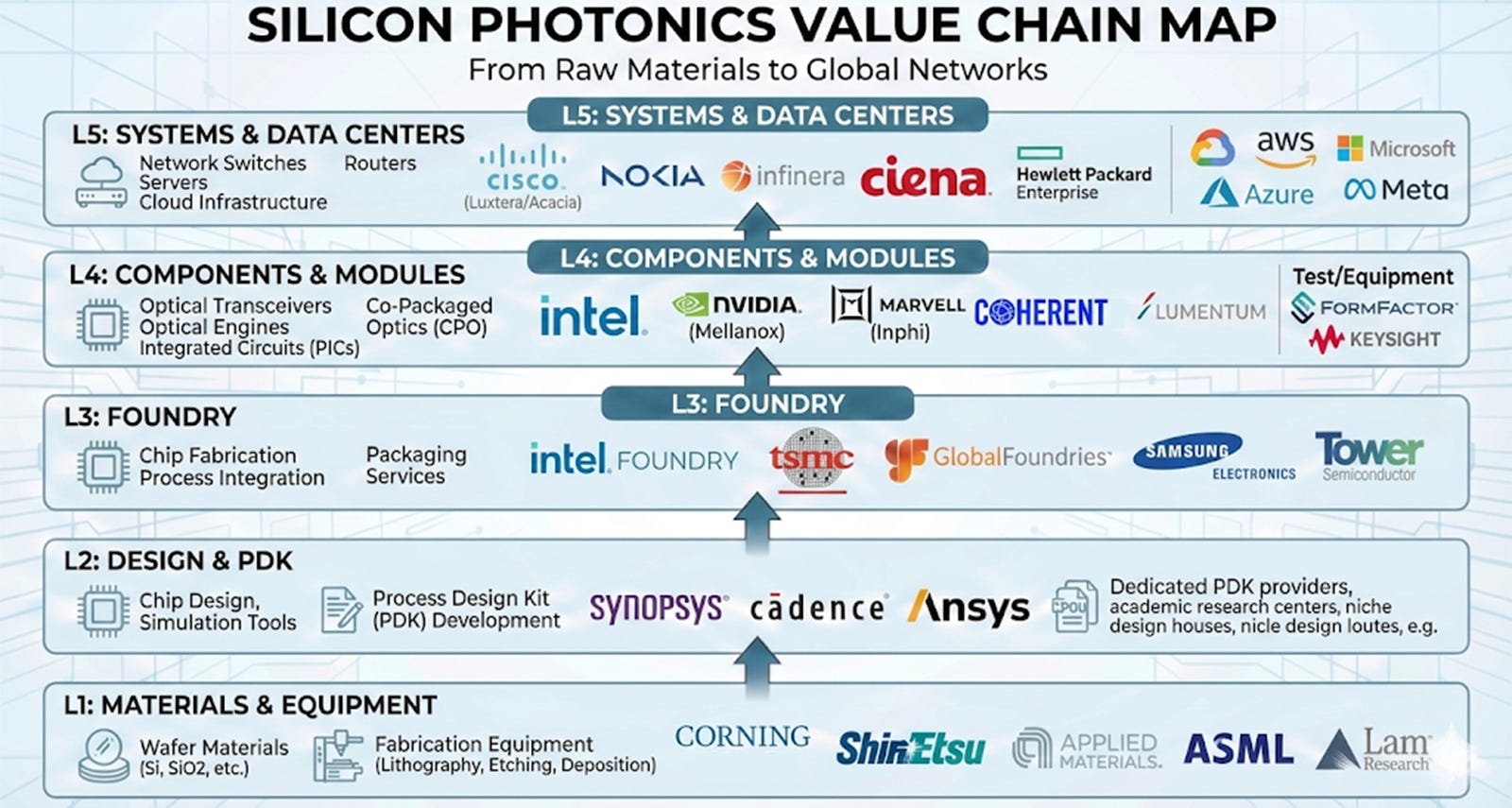
4. Expanding Ecosystem: Who Leads the Market?
Until the 2010s, conservative forecasts dominated, viewing the silicon photonics market as merely a ‘distant future technology’ or a ‘niche market’. It was a time when large-scale investment was hesitant due to technical challenges and unclear economic viability.
However, the massive wave of the AI revolution changed everything. As of 2026, silicon photonics has completely transcended the stage of being merely a ‘research project’. It has rapidly emerged as essential core infrastructure for AI data centers to handle explosive data traffic, propelling the market into a powerful inflection point where it has bottomed out and is now surging upward.
According to recent market research (Verified Market Research, etc.), the silicon photonics market is projected to grow at an astonishing compound annual growth rate (CAGR) of 25.5% until 2032, reaching revenues exceeding approximately $10.5 billion. As the market matures, players in each sector—design, foundry, testing, materials—are differentiating themselves more precisely, forming a vast industrial ecosystem.
① Design and Foundry: “The Brain and Heart of the Fabless Revolution”
The Brains (EDA/Design): Ansys, which owns Lumerical—the standard in optical simulation—recently merged with EDA giant Synopsys ($SNPS), giving birth to a massive platform integrating electronic and photonic design into a single workflow. Cadence ($CDNS) is also aggressively integrating optical PDKs into its tools. This has ushered in an era where designers can assemble chips like Lego blocks without needing deep knowledge of complex physical laws.
The Foundry: TSMC ($TSM) is strengthening its foundry leadership, now encompassing optical chip packaging, spearheaded by its COUPE technology. GlobalFoundries ($GFS) and Tower Semiconductor ($TSEM) are transforming depreciated legacy processes into dedicated silicon photonics lines, securing overwhelming profitability.
② Platform and Chip Leaders: “The Dominant Players in CPO and Next-Generation Interconnects”
Intel ($INTC): A pioneer that has led the market for over 20 years since announcing the world’s first gigahertz-class modulator in 2004. Its ‘hybrid silicon laser’ technology, which directly bonds indium phosphide (InP) lasers onto silicon wafers, is the global benchmark for light source integration and currently dominates the 800G/1.6T transceiver market.
Nvidia ($NVDA) & Broadcom ($AVGO): To resolve bottlenecks within AI servers, they are positioning Co-Packaged Optics (CPO) as a core element of their next-generation roadmap. Broadcom is actively supplying solutions to big tech companies like Google with its ‘Bailly’ platform, which integrates optical engines into ‘Tomahawk’ switches. Nvidia has built its next-generation interconnect roadmap by transplanting Mellanox’s technological capabilities to directly connect GPUs with optical links.
Marvell ($MRVL): The PAM4 DSP technology from ‘Inphi’, acquired for $10 billion, is Marvell’s core weapon. DSP, which corrects light signal distortion, serves as the essential ‘brain’ of high-speed networks. Recently absorbing Celestial AI technology, Marvell has emerged as a leader in ‘photonics fabric’ architecture, optically connecting memory and computation.
③ Light Sources & System Integration: “The Infrastructure Giants”
Coherent ($COHR) & Lumentum ($LITE): These are the absolute leaders in the external light source (ELS) market, supplying the light that is the ‘heart’ of silicon photonics. However, their true strength lies in their vertical integration, spanning from optical materials like indium phosphide (InP) to finished modules. They are the reliable suppliers of lasers for silicon photonics chips.
Nokia ($NOK): By completing its acquisition of Infinera in 2025, it became a tech titan possessing both silicon photonics technology and a global telecommunications infrastructure sales network. It now competes with Cisco for supremacy in the next-generation optical network market.
Cisco ($CSCO): By acquiring Luxtera, a pioneer in silicon photonics mass production, and Acacia, known for coherent technology, Cisco has long demonstrated the power of ‘internalized optical technology’.
④ Testing and Packaging: “Gatekeepers of Commercial Yield”
FormFactor ($FORM): Silicon photonics requires measuring ‘light’ at the wafer stage, making testing extremely difficult. FormFactor recently acquired Keystone Photonics, solidifying its optical testing leadership and holding the key to securing mass production yields.
Corning ($GLW ): Provides precision packaging solutions connecting chips and optical fibers, responsible for the physical data transmission pathway.
5. PhotonCap’s Insight
Investors must look beyond simply ‘who makes the chips’ and instead focus on ‘who most efficiently transitions existing infrastructure to silicon photonics’.
First, companies like Coherent and Lumentum enjoy a monopoly position supplying the ‘light (laser)’—the heart of silicon photonics. Additionally, giants like Nokia, which recently acquired Infinera, are aggressively moving to absorb technology-driven companies to control entire systems. Their vast customer networks and patent portfolios form a formidable moat that startups cannot easily breach.
Particularly noteworthy are test equipment companies like FormFactor. Silicon photonics is a technology where ‘verification and packaging’ are far more challenging than design. The ability to accurately measure light loss at the wafer level and secure yield is the final hurdle for silicon photonics to leap from the lab to commercial success. It’s crucial to remember that “those selling jeans and pickaxes (test/equipment)” can offer a safer and more reliable revenue model than “those mining the gold (fabless companies).”
Finally, keep an eye on small but powerful companies dreaming of disruptive innovation. Players like POET Technologies (not shown in the Value Chain Map), aiming for a packaging cost revolution with optical interposer platforms, and Aeluma, seeking to transform manufacturing processes by growing lasers directly on silicon wafers, are accelerating silicon photonics’ ‘golden age for commercialization’. These two companies are noteworthy for their innovations in ‘packaging/platform’ and ‘materials/growth’ aspects, respectively. Additionally, companies like Ayar Labs, which offer solutions connecting chips with light, should also be examined.
6. References
• Charles K. Kao Nobel Prize lecture https://www.nobelprize.org/prizes/physics/2009/kao/lecture/
• Chrostowski, L., & Hochberg, M. (2015). Silicon Photonics Design. Cambridge University Press. (Chapters 1.1, 1.2, 1.5)
• Liu, A., Jones, R., Liao, L.et al.A high-speed silicon optical modulator based on a metal–oxide–semiconductor capacitor.Nature427**, 615–618 (2004). https://doi.org/10.1038/nature02310
• Verified Market Research. “Silicon Photonics Market Size and Forecast”. https://www.globenewswire.com/news-release/2026/01/13/3217445/0/en/Silicon-Photonics-Market-is-expected-to-generate-a-revenue-of-USD-10-48-Billion-by-2032-Globally-at-25-50-CAGR-Verified-Market-Research.html
• YOLE Group. “Silicon photonics drives ultra high bandwidth boosts, scaling AI networks as the market jumps from $278M in 2024 to $2.7B by 2030, a 46% CAGR.” https://www.yolegroup.com/product/report/silicon-photonics-2025---focus-on-soi-sin-and-lnoi-platforms/
A great article, thank you! I just wanted to mention Halma plc. They have a subsidiary called Avo Photonics buried within the business that is working with a hyperscaler and has been for over 10 years. Their business is growing rapidly.
https://rogerbreuer.substack.com/p/halma-plc-from-tea-plantations-to?r=1qxcim
Wow, I literally grew up looking up to Charles Kao, the only Hong Konger who won a Nobel Prize to date. He was lionized in Hong Kong and British media.