
P = I²R: The One-Line Equation Shaping AI Infrastructure and Vicor's ($VICR) VPD
Why the architecture that lost the H100 socket could win the CPO era
Note. As mentioned in an earlier X post, I first came across $VICR in November 2025 thanks to @butchertrader, studied and bought the stock, then sold my entire position in January 2026 after concluding I hadn't done enough homework. This piece is the study material I put together to get ready to buy it again.

Abstract
Next-generation AI accelerators demand roughly 1000A steady-state and 2000A peak current at a core voltage of about 0.7V. Because of P = I²R, tens of watts per module evaporate as heat while that current traverses the “last inch” of copper on the PCB. Vicor’s ($VICR) Factorized Power Architecture (FPA) and Vertical Power Delivery (VPD) attack this segment, cutting PDN (power delivery network) impedance by up to 50× versus conventional multiphase solutions. This piece starts from P = I²R and works through (1) a decomposition of PDN losses, (2) how FPA and the SAC topology work, (3) the transition from LPD to VPD and the GCM structure, (4) the design intent behind ChiP packaging, (5) the space and thermal constraints that co-packaged optics (CPO) bring, (6) the thermo-optic sensitivity of micro-ring resonators and why VPD pairs with it, and (7) a quantitative analysis centered on NVIDIA’s Quantum-X, with comparison points to Broadcom’s Tomahawk CPO line (Bailly, Davisson).
Contents
Intro: The weight of a one-line equation
The company called Vicor
2.1 Founding and governance
2.2 Business structure and financial snapshot
2.3 Position in the competitive landscape
Problem definition: P = I²R and the last inch
3.1 Delivering 0.7V × 2000A through the last inch
3.2 Decomposing PDN impedance
3.3 The limits of conventional solutions: multiphase buck and TLVR
Vicor’s answer: FPA, SAC, ChiP
4.1 FPA: separating regulation from transformation
4.2 SAC topology: why a sine amplitude converter
4.3 From LPD to VPD: moving the conversion point under the processor (paid)
4.4 GCM structure: gearbox and BGA pin mapping (paid)
4.5 ChiP packaging: heat extraction and EMI shielding (paid)
Where CPO meets VPD
5.1 CPO overview: the ASIC + PIC + ELS package (paid)
5.2 The optical power budget: ELS, coupling loss, micro-ring modulator (paid)
5.3 The thermal problem: 1°C produces an 80 pm shift (paid)
5.4 Why CPO and VPD end up bound together (paid)
5.5 Quantitative analysis: the NVIDIA Quantum-X case (paid)
Closing
References & Sources
1. Intro: The weight of a one-line equation
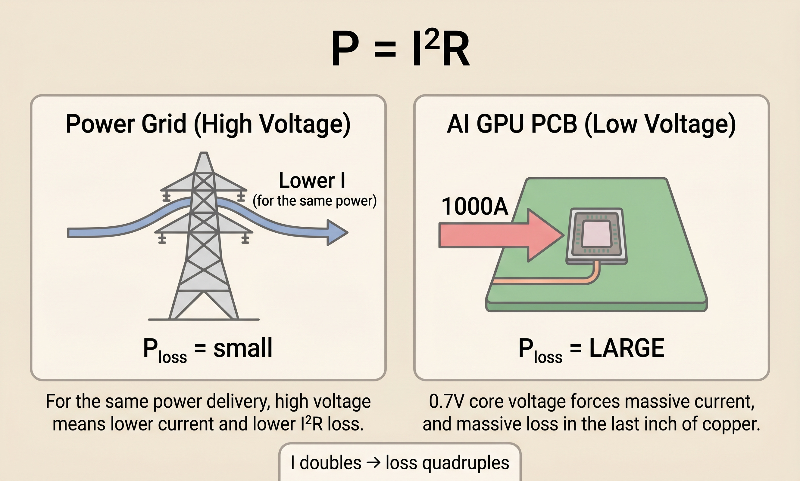
V = IR. Ohm’s law, the one most of us learned back in school. Pair it with another basic equation, P = V × I (power equals voltage times current), and substitute IR for V. You get P = I²R. Power loss in a resistor scales with the square of the current. Double the current and the loss quadruples. Ten times the current, a hundred times the loss.
This one equation from physics class now defines the physical limits of AI infrastructure. The bottleneck is not only FLOPS. Compute performance and memory bandwidth are already well-known constraints, and power delivery itself has joined them as a first-order limit. The core of this new limit is the last inch of copper that has to carry over 1000A at 0.7V into the processor, and co-packaged optics (CPO) is turning that copper problem back into a game for power module companies.
Current-generation AI accelerators pack anywhere from 80 billion transistors (H100, on TSMC 4N) to 208 billion or more (Blackwell B200, on TSMC 4NP) into a single die. The core supply voltage (VDD) has dropped to around 0.7V.[1] Yet the same chip demands 1000A steady-state and 2000A peak current.[1] That translates to roughly 700W continuous and 1400W peak power events. The transient side is even harder. Under the load swings of neural network workloads, current slews at 2000A/μs, and during those swings the supply voltage must stay within ±10% (about 0.07V) overshoot and undershoot to keep the transistors alive.[1]
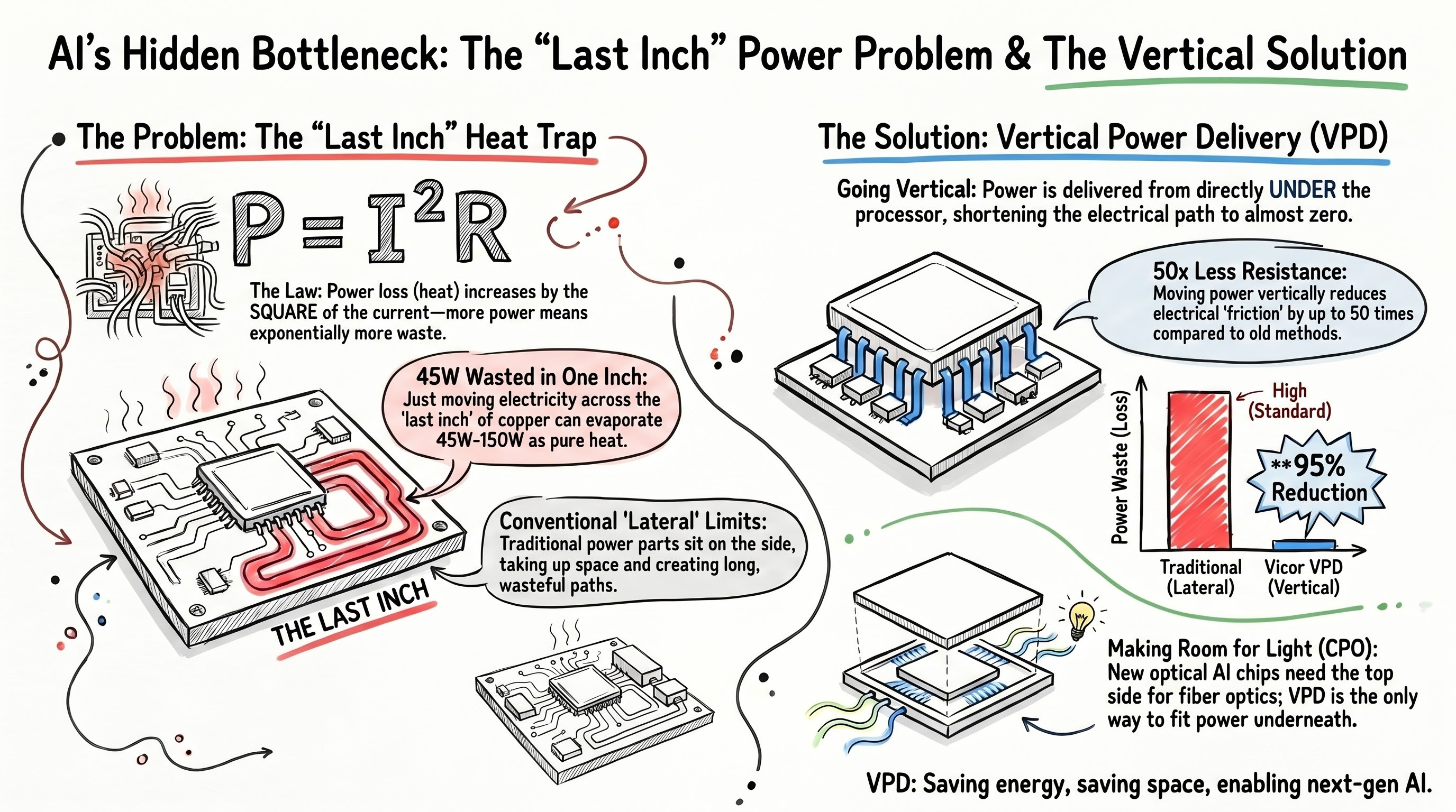
This is where P = I²R goes to work, mercilessly. Even if the last segment of resistance between the PCB and the processor is only 70 microhms (µΩ), pushing 800A through it costs about 45W.[2] That loss is not from the compute, not from moving data to memory. It is just current passing through copper.
This article is about how that loss gets reduced. It takes a look at how Vicor’s ($VICR) Factorized Power Architecture and Vertical Power Delivery, developed over three decades, attack that one-line equation, and why the answer becomes decisive again in the CPO era.
[Figure 1: Intuitive diagram of P = I²R, transmission line vs. PCB]
2. The company called Vicor
Before jumping into the technical analysis, a quick orientation on the company itself.
2.1 Founding and governance
Vicor Corporation was founded in 1981 in Andover, Massachusetts, by Dr. Patrizio Vinciarelli.[3] Vinciarelli earned his PhD in physics from the University of Rome, served as a fellow at CERN from 1973 to 1976 researching particle physics, and moved to the United States to hold fellow and instructor positions at the Institute for Advanced Study and Princeton University before founding Vicor in 1981. In interviews, he has described frustration with the limits of academia as what pushed him into power conversion as an industry. He personally holds more than 150 patents in power conversion and received the 2019 IEEE William E. Newell Power Electronics Award. The award citation reads “for visionary leadership in the development of high-efficiency, high-power-density power conversion components for distributed power system applications.”[3]
One governance detail worth flagging. Vicor has a dual-class structure with Common Stock and Class B Common Stock. Class B carries 10 votes per share versus 1 for Common, and is held almost entirely by Vinciarelli. Per the 2025 year-end 10-K, roughly 11.72 million Class B shares are outstanding.[4] Between his Common and Class B holdings, Vinciarelli controls roughly 47% of the economic interest and about 80% of the voting power.[4] In other words, the 44-year-old founder-CEO structure is not symbolic. It is rooted in voting control.
2.2 Business structure and financial snapshot
Vicor listed on NASDAQ in April 1990 (ticker VICR), and its headquarters along with all core manufacturing sits in Andover, Massachusetts. The company frames in-U.S., vertically integrated manufacturing as a core differentiator. A new ChiP fab in Andover went live in 2018, expanding capacity roughly 2.5×, and an additional fab (referred to as Fab 5) is in progress.
Revenue splits three ways. In fiscal year 2025, product revenue was $350.3M, up 12.1% year over year, with royalty revenue of $57.4M (+23.2%) and a $45M patent litigation settlement bringing total annual revenue to $452.7M.[5] Product revenue itself breaks into two segments: the Brick Products segment, with traditional brick form-factor DC-DC converters for industrial, aerospace/defense, and telecom infrastructure, and the Advanced Products segment, with ChiP-based modules including the VPD/LPD solutions that go into AI/HPC data centers. Royalty revenue comes from licensing Vicor’s patents to other power module manufacturers. That creates a structure where, as AI accelerator power modules sell, Vicor benefits both from its own product revenue and from royalties paid by competitors. Q4 2025 posted product revenue of $92.7M, gross margin of 55.4%, and net income of $46.5M ($1.01 EPS), with full-year net income of $118.6M ($2.61 EPS).[5]
Financial snapshot in numbers (all as of the 2026-04-17 close): share price $218.05, market cap roughly $9.89B, 52-week range from $38.93 to $224.76. Trailing P/E sits in the 83 to 85 area, TTM net margin 26.2%, gross margin 57.3%. Cash and cash equivalents were $402.8M as of Q4 2025, with a debt/equity ratio of 0.01, effectively net cash. Headcount is around 1,000. A P/E in the 80s is firmly in highly-priced territory, and the stock is up roughly 5.6× from $38.93 a year ago. One reading is that the market is pricing in the Gen 5 VPD ramp and a rise in licensing revenue ahead of time. P/S works out to roughly 22× revenue. Q1 2026 earnings are scheduled for 2026-04-21.[6] Price figures are volatile and should be read as a snapshot.
2.3 Position in the competitive landscape
On competition, the power module market splits into two camps. On one side are integrated semiconductor IDMs: Texas Instruments ($TXN, with roughly 12.5% of global PMIC revenue share), Analog Devices ($ADI), Infineon ($IFNNY), Renesas ($RNECY), STMicroelectronics ($STM), and NXP ($NXPI).[7] They carry broad catalogs and thick bases in automotive and industrial markets. On the other side are power-specialized players: Monolithic Power Systems ($MPWR), Power Integrations ($POWI), and Vicor itself. MPWR in particular is widely regarded as having captured the majority of AI accelerator power sockets.
Vicor’s position inside this landscape is distinctive. On absolute share of the AI accelerator power market, the market view is that MPWR has taken the larger socket.[8] MPWR locked in that position with the cost structure of multi-phase buck solutions and the simplicity of lateral integration. Vicor’s VPD is technically more sophisticated but has faced a longer adoption cycle and heavier reliance on a single lead customer. In return, Vicor carries in-U.S. vertically integrated manufacturing, a thick patent portfolio around FPA/SAC/ChiP (the foundation of the licensing revenue), and a technical edge in structurally high-current, high-voltage territory like 800V distribution, automotive Gen 5, and AI VPD. Brick products deliver long-tail revenue in industrial and aerospace/defense, while Advanced Products and royalties act as the growth driver tied to the AI infrastructure cycle. It is a dual structure.
In summary, Vicor is an Andover, Massachusetts-based power module specialist founded in 1981 by founder-CEO Patrizio Vinciarelli. FY2025 revenue of $452.7M, net margin 26%, market cap in the $10B range makes it a mid-cap. A P/E in the 80s reflects the market pricing in the Gen 5 VPD ramp and licensing revenue up front. On absolute share of AI accelerator power, MPWR leads. But Vicor holds differentiated position through in-U.S. manufacturing, its patent portfolio, and structural strongholds in areas like 800V distribution. Now into the technical core.
3. Problem definition: P = I²R and the last inch
3.1 Delivering 0.7V × 2000A through the last inch
Why do AI accelerators demand such a low voltage at such a high current? Two reasons.
First, transistor scaling. As process nodes move from 7nm to 5nm to 4nm to 3nm, transistor gate oxide thins out, and the upper limit of the supply voltage that can switch the transistor reliably comes down. At 4nm, core voltage sits around 0.7V.[1] There is not much room to push it lower. The noise margin and transistor reliability limits take over.
Second, transistor count. More transistors on the same die means more transistors switching simultaneously, and leakage current accumulates too. As noted earlier, current-generation AI accelerators integrate roughly 80 billion to 208 billion transistors in a 4nm-class process, and at that level chip-level current crosses 1000A easily.[1]
Since P = V × I and V cannot go lower, I has to rise to deliver the same P. The result is 1000A steady-state, 2000A peak.
An intuition check. Why do power transmission lines run at hundreds of thousands of volts? For the same power delivered, higher voltage means lower current, and lower current squared means exponentially lower P = I²R loss. From power plant to transmission tower, electricity flows at high voltage and low current, and only at the neighborhood level does the transformer step it down. Data centers follow the same principle, moving from 12V to 48V and now toward 800V DC distribution.[1]
The problem is the final step. Somewhere, 48V (or 800V) has to be stepped down to 0.7V, and the farther that conversion point sits from the processor, the larger the P = I²R loss becomes. The industry calls this final segment the “last inch.” For a standard 60×60mm AI processor package, even sitting a voltage regulator right at the package edge still leaves about 30mm of PCB path to the core.[9]
One more variable. Transients. The load swings from 0 to 2000A in under a microsecond, and if voltage deviates more than ±10% during that swing, the transistors take damage. That requires around 3mF of decoupling capacitance directly under the processor package.[1] Where those capacitors physically fit becomes another design conflict.
The problem is this. AI accelerators demand low-voltage high-current (0.7V × 1000A+) and 2000A/μs transients simultaneously. Meeting that requires (1) moving the conversion point close to the processor, (2) placing decoupling capacitors directly beneath the processor, and (3) minimizing PDN impedance aggressively. Solving any one creates tension with the others.
3.2 Decomposing PDN impedance
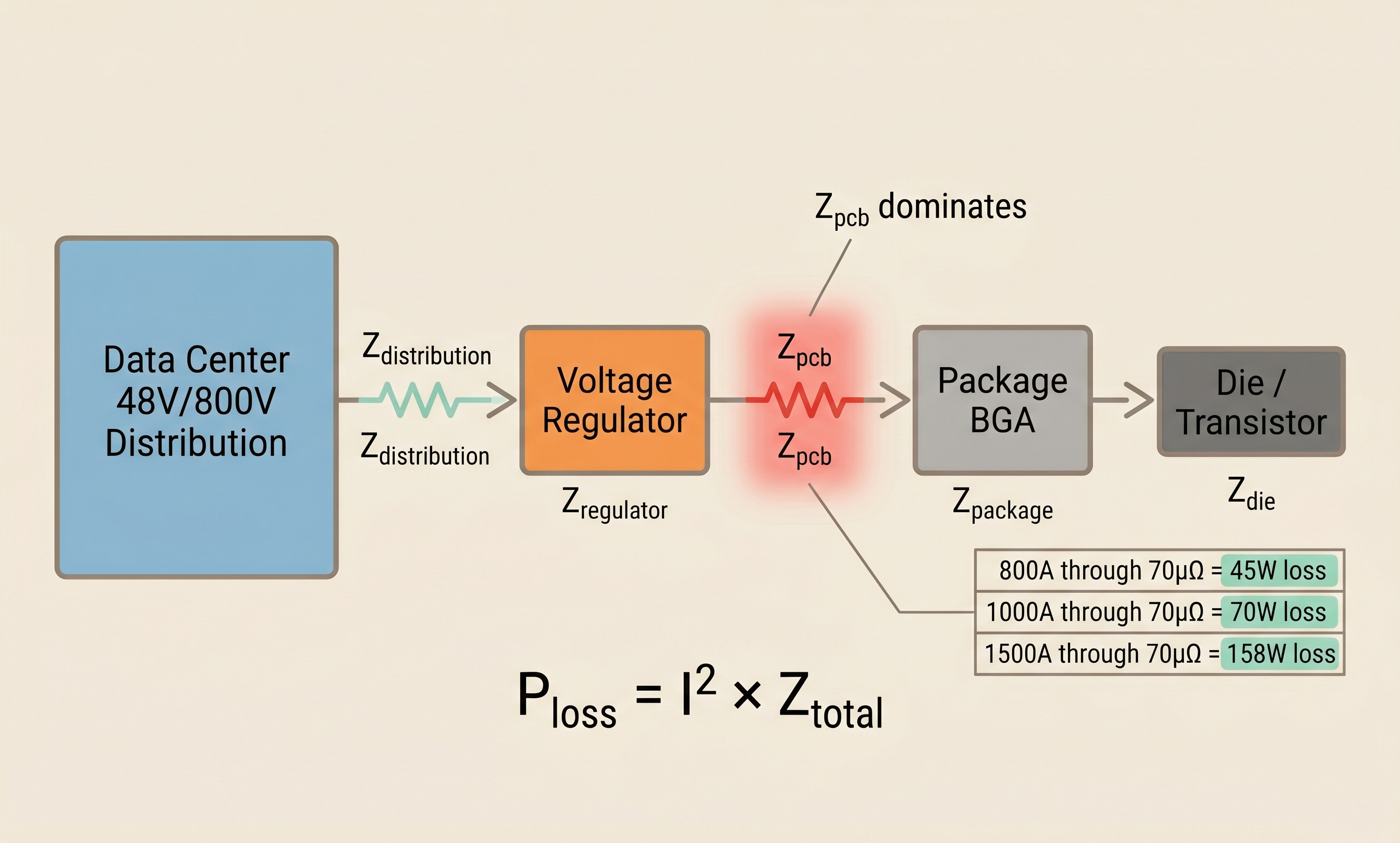
The PDN (power delivery network) is the full path from the power source to the transistor. Its total impedance Z_total is the sum of several components.
Z_total = Z_distribution + Z_regulator + Z_pcb + Z_package + Z_dieBreaking down the loss each component contributes shows where P = I²R hits hardest.
Z_distribution: data center power to rack. The 12V vs 48V choice is decisive. Delivering the same power at 12V means 4× the current and 16× the loss versus 48V.
Z_regulator: conversion loss in the voltage regulator itself. 95% efficiency means 5% loss.
Z_pcb: trace resistance on the PCB. Copper sheet resistance × length / width.
Z_package: BGA pins and redistribution layer inside the processor package substrate.
Z_die: metal layers and TSVs inside the die.
To revisit, from a PDN perspective, the example from Section 1. At 100°C, with a voltage regulator at the edge of a 60×60mm processor package pushing 800A through the PCB, assuming 70µΩ of trace resistance, the loss is 800² × 70 × 10⁻⁶ = about 45W.[2] That is loss from a single PCB segment alone. This is why Z_pcb dominates total PDN loss.
If current rises to 1000A, the loss at the same resistance becomes 70W. At 1500A, 158W. The current increase drives loss up as a square. This is why, for multi-kilowatt AI accelerators, PDN design is essentially system efficiency itself.
Two ways to reduce Z_pcb. Make traces thicker, or make the distance shorter. Thickening traces eats PCB area and cost and hits hard limits. That leaves the other option: shortening the distance, which means bringing the voltage regulator closer to the processor. Ideally, directly underneath. That direction converges on VPD (Vertical Power Delivery).
[Figure 2: PDN impedance decomposition]
3.3 The limits of conventional solutions: multiphase buck and TLVR
The industry-standard solution is the multiphase buck regulator. It steps down 12V or 48V input to 0.7V by sharing the job across parallel inductors and switches. Each phase switches with an offset to reduce output ripple, and together they deliver large current.
A recent variant in GenAI accelerator modules is the TLVR (trans-inductor voltage regulator), a buck topology that magnetically couples the inductors to speed up transient response. In theory, it works.
The problem is scaling.
As current rises, more phases are needed. For 1000A, assuming 50A per phase, roughly 20 phases. Each phase requires a separate inductor, switch, control IC, and cooling path. Modular integration is low.[9]
That grows PCB area, and the larger area pushes the voltage regulator farther from the processor. More distance means higher Z_pcb, which means higher P = I²R loss. The contradiction is that adding phases to handle more power ends up increasing the loss that drove the need.
Another limit. Multiphase PWM (pulse-width modulation) buck is fundamentally current averaging. It creates an average current by switching phases on and off with time offsets. That approach has a response-speed limit. To handle 2000A/μs transients, more decoupling capacitors are needed, and those capacitors again occupy space around the processor.[1]
All of these tensions point in one direction. As long as the conversion point stays separated from the processor, the problem does not resolve. This is where Vicor proposed a different answer.
The important point here. Multiphase buck and TLVR scale current by adding phases, but adding phases consumes PCB space, and the space consumed pushes the conversion point farther from the processor, where P = I²R loss rises again. A self-contradiction.
4. Vicor’s answer: FPA, SAC, ChiP
4.1 FPA: separating regulation from transformation
The core idea of Factorized Power Architecture boils down to one sentence. Physically separate regulation (voltage control) from transformation (voltage conversion).[10][11]
A typical buck regulator handles both inside a single module. Neither function gets optimized. Regulation needs a precise feedback loop and fast response, which requires a stable location for the controller. Transformation handles large current and heat, and gets closer to the processor as PDN loss drops. The two requirements conflict inside one module.
FPA separates them and places each at its optimal location.
PRM (Pre-Regulator Module): regulates input voltage to a stable intermediate voltage (the “Factorized Bus”). Can sit anywhere on the motherboard. Optimized for response speed and accuracy.
VTM (Voltage Transformation Module) or GCM (Geared Current Multiplier): takes the Factorized Bus, steps voltage down by a factor of K, and multiplies current by K on the way into the processor. Sits directly next to or beneath the processor. Optimized for current density and PDN distance.
The K factor is the multiplication ratio of the current multiplier. For K = 1/48, an input of 48V becomes 1V output, and input current X becomes 48X on output. Impedance seen from the input side appears K² times smaller on the output side.[10]
One number that captures what this separation produces. Combined PRM and VTM system efficiency runs 90% to 95%, and a single VTM’s output impedance (R_OUT) can reach as low as 0.8 milliohms (mΩ).[11] 0.8 milliohms is an order of magnitude below conventional multiphase impedance.
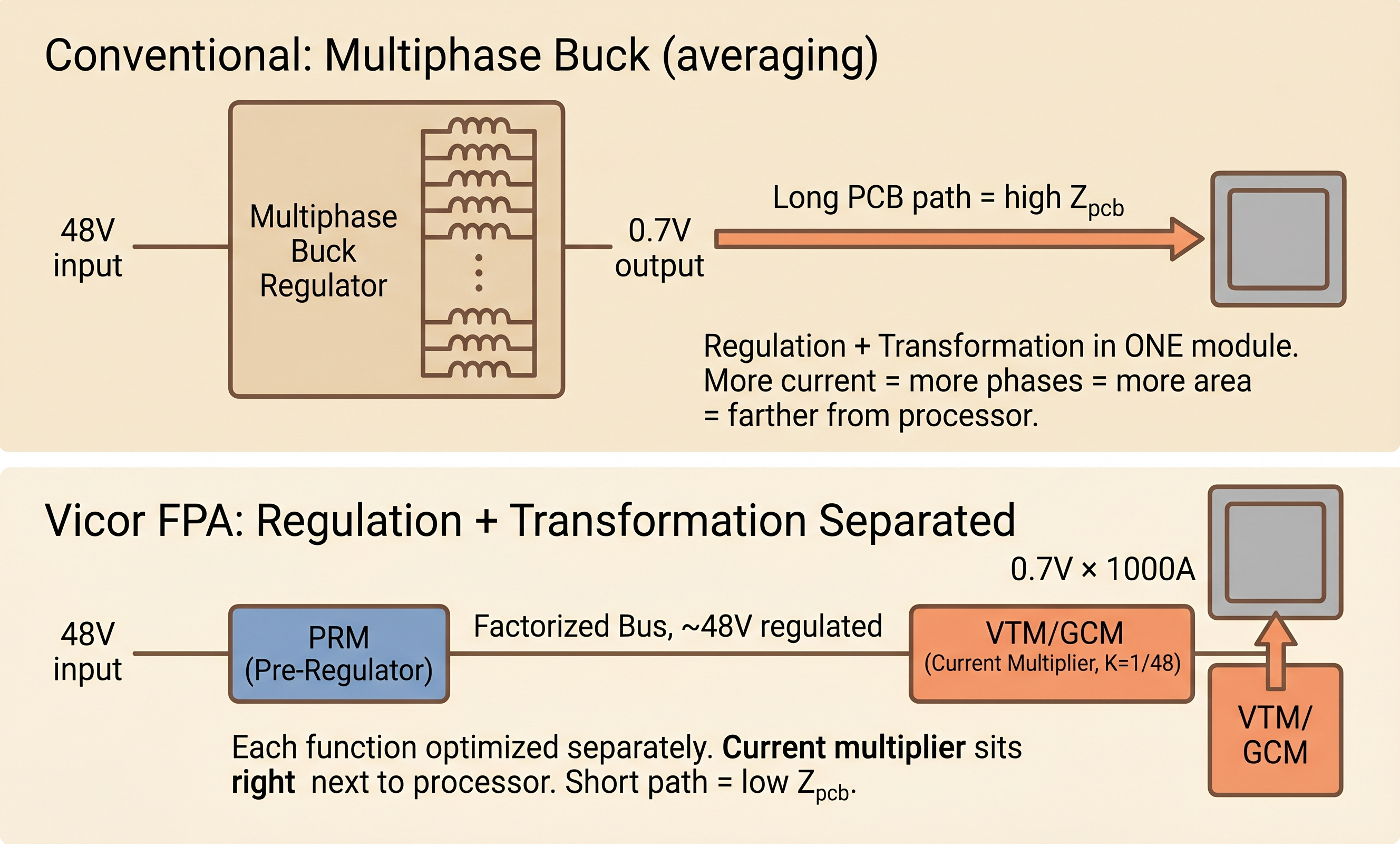
[Figure 3: Multiphase buck vs FPA structure comparison]
4.2 SAC topology: why a sine amplitude converter
If FPA is the architecture, SAC (Sine Amplitude Converter) is the circuit topology that actually implements it.[10][12]
SAC boils down to two words. Resonant + fixed-ratio.
A standard PWM buck hard-switches the transistors. It turns them on and off while current and voltage are both large. That creates switching loss, and voltage spikes from interrupted inductor current produce significant EMI (electromagnetic interference).
SAC is different. It operates under ZCS (Zero-Current Switching) + ZVS (Zero-Voltage Switching) conditions.[10] An LC tank formed from a transformer and a resonant capacitor produces a sinusoidal current waveform at its natural resonant frequency, and the controller times the switching precisely at the waveform’s zero crossings. Switching happens at the moment current (or voltage) is zero, so switching loss is minimal. Efficiency reaches around 97%.[11]
The other feature is fixed-ratio. Unlike a typical regulator that adjusts output voltage variably, the K ratio (e.g., 1/48) is fixed. This sounds like a drawback but is actually a major advantage.
No control loop burden: no fast feedback loop for output voltage regulation means response speed is set by the circuit’s resonant frequency itself.
Wide bandwidth: on a VTM module, effective switching frequency is around 3.5 MHz, and output impedance stays flat out to about 1 MHz.[10] Load variations below 1 MHz get near-instant response.
Sub-microsecond load response: 1μs or less to a load step.[11] This is the decisive reason why 2000A/μs transients can be handled.
And the sinusoidal waveform carries far less harmonic content than PWM’s square waves, so EMI emissions are fundamentally lower.[10] That’s a large signal-integrity advantage on high-density boards.
To put the whole flow together: PRM turns input voltage into a stable Factorized Bus (e.g., 48V regulated), and VTM or GCM steps that bus down by 1/K while multiplying current by K and feeding the processor. PRM can go anywhere on the PCB, while VTM/GCM sits next to or directly beneath the processor. Total system efficiency 90% to 95%, single-VTM output impedance around 0.8 mΩ.[11]
The SAC dynamics in one line. SAC is a fixed-ratio resonant converter operating under ZCS/ZVS, achieving 97% efficiency, sub-microsecond response time, and output impedance as low as 0.8 mΩ. It produces a dynamic region hard-switching PWM buck cannot reach, and that behavior is the foundation that turns FPA into a real product.
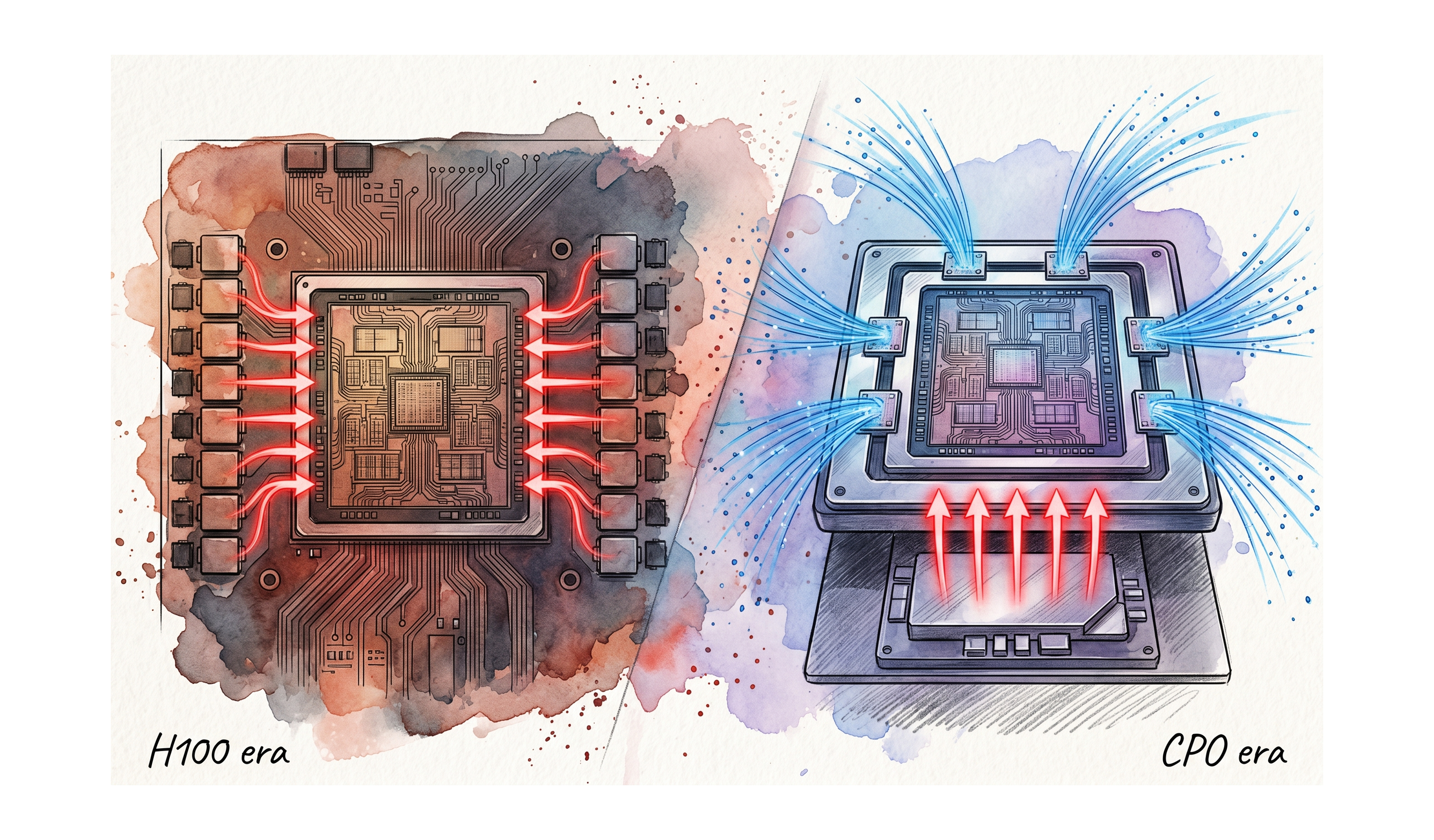
That closes out the free section. We have walked through the 0.7V × 2000A problem, the PDN impedance decomposition, the limits of conventional solutions, and the different answer Vicor’s FPA + SAC provides. But the problem does not end here. Once optics starts sitting next to the ASIC, the lateral power delivery familiar from the H100 era physically loses its footing. The story of VPD almost landing in the H100 socket, then losing it to MPWR’s multiphase solution, is well known, but the point is that the structure that lost on cost and manufacturing ease in H100 could actually be advantaged in CPO.
But how much of “could be advantaged” is technical inference, and how much shows up in actual numbers? What happens when you decompose NVIDIA’s officially disclosed 9W per port and tens-of-megawatts data center savings through the lens of power delivery architecture? And where does something like Vicor’s GCM sit in that decomposition? We unpack each of these below.
4.3 From LPD to VPD: moving the conversion point under the processor (paid)
Within FPA, where the current multiplier (VTM or GCM) gets placed yields two options.
LPD (Lateral Power Delivery): VTM modules flank the processor on its left and right (or top and bottom). Effective up to roughly 800A.[11] At an 800A 0.8V load with about 70µΩ PDN resistance, loss is around 45W.[11] Delivering current from both sides cuts loss 50% versus one-sided delivery.
VPD (Vertical Power Delivery): The conversion part of the GCM (Geared Current Multiplier), meaning the VTM Array + Gearbox, sits directly beneath the processor on the opposite side of the PCB, while the PRM sits remotely elsewhere. VPD comes into its own above 1000A. From here on, “VPD” refers to this placement method as a whole, and “VPD module” or “GCM” refers specifically to the conversion part that sits directly beneath the processor.
Three quantitative advantages of VPD over LPD.
Lower PDN impedance: VPD reduces PDN impedance by roughly 20× versus a conventional lateral arrangement.[1] Combining FPA + VPD against a typical multiphase buck PCB solution, Vicor reports up to 50× PDN resistance reduction.[9] A 50× factor goes straight into P = I²R, meaning the same current produces 50× lower loss.
Roughly 100W saved per module: on a GenAI accelerator module, Vicor estimates that factorized VPD saves about 100W versus a TLVR-based lateral solution.[1] Across a 20,000-accelerator-module supercomputer, that is 2MW, or roughly 17.5 GWh annually at 24/7 operation, worth millions of dollars at industrial power rates.[1]
Topside space freed: moving the conversion module under the processor opens up 100% of the PCB area above the processor.[13] That space becomes available for high-speed I/O, memory routing, and, as we will see, optical I/O placement.
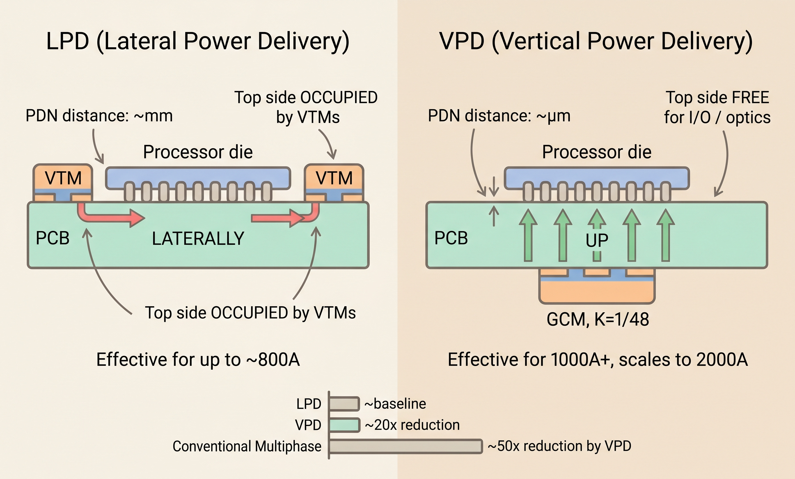
[Figure 4: LPD vs VPD cross-section]
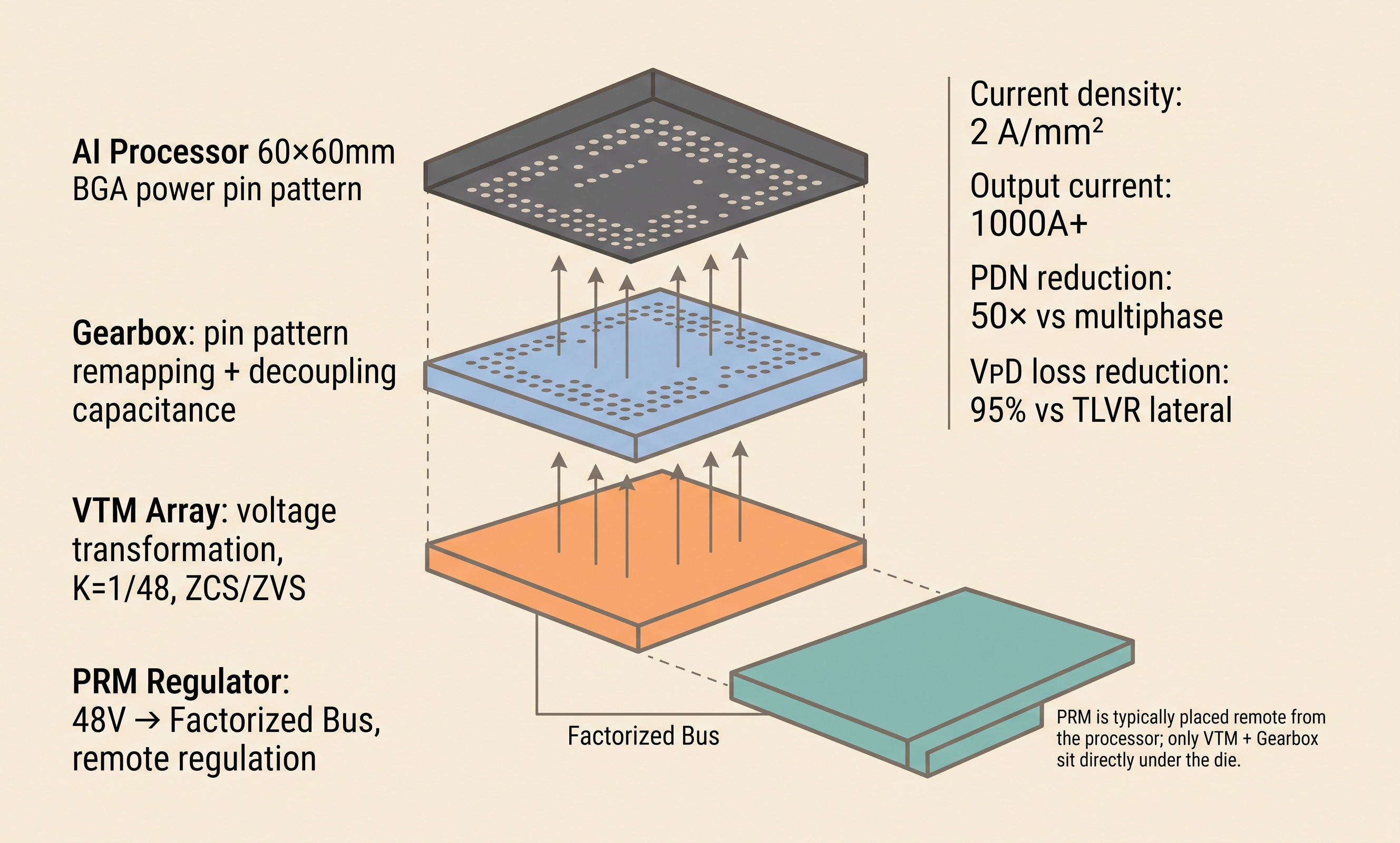
4.4 GCM structure: gearbox and BGA pin mapping (paid)
VPD doesn’t end at “put the current multiplier under the processor.” In practice, it has to solve two additional problems simultaneously.
Problem 1: Where decoupling capacitors go
Directly under the processor is normally the space for high-frequency decoupling capacitors (>10MHz).[14] Roughly 3mF of decoupling capacitance needs to sit close to the processor package to absorb transient load swings. But VPD needs that same space. A conflict.
Problem 2: Pin-map mapping
A VTM module’s output pin pattern is determined by its internal circuit structure, while the processor’s power input pin pattern (BGA) is determined by the die’s power map. They usually don’t match. Connecting the two patterns directly causes asymmetry, with some pins carrying much more current than others, dropping efficiency.
GCM (Geared Current Multiplier) is the structure that solves both problems at once.[14] The vertical stack that sits directly beneath the processor is layered, top to bottom, as follows.
Gearbox (topmost, directly under the processor): performs two functions simultaneously
Remaps the current multiplier’s output pin pattern onto the processor’s power pin map (solves the pin-map mapping problem)
Integrates high-frequency decoupling capacitance inside the module itself (solves the decoupling-space problem)
VTM Current Multiplier Array (below the Gearbox): SAC-based fixed-ratio conversion, stepping the Factorized Bus down by 1/K and supplying K× current
And the PRM Regulator is NOT part of this vertical stack. It sits remotely on another location on the board. It takes the 48V input, creates the stable Factorized Bus, and feeds it to the VTM Array. The FPA principle of separating regulation from transformation shows up physically in the placement as well.
The name Gearbox is meaningful. Just as a car’s gearbox converts engine rotation into wheel rotation, the Gearbox converts the current multiplier’s output pattern into the processor’s power pattern.
The quantitative results this structure produces.[15]
Current density around 2 A/mm²: a 1cm × 1cm GCM can deliver 200A
Output current 1000A+: on a single module
Interconnect loss reduced by up to 90%: with substrate-level integration (Vicor + Kyocera)[13]
VPD loss reduction of 95%: versus TLVR lateral[15]
[Figure 5: GCM internal structure (PRM + VTM Array + Gearbox)]
