
Marvell Acquires Swiss Plasmonics Startup Polariton: A Decade-Old Promise Returns, and LWLG is Inside
Plasmonics was written off eight years ago. It just landed at the center of Marvell's 3.2T roadmap, with LWLG's Perkinamine inside
Abstract
On April 22, 2026, Marvell (NASDAQ: MRVL) announced the acquisition of Polariton Technologies, a Swiss spinoff from ETH Zurich. Financial terms were not disclosed. This article traces how plasmonics, a field that swept academia in the 2010s and seemed to quietly disappear, found its way back to the center of a major semiconductor company’s optical roadmap in 2026, and how this acquisition creates a structural link between Marvell and Lightwave Logic (LWLG). Related tickers: $MRVL, $AVGO, $COHR, $LITE, $LWLG.
Contents
Marvell’s Optical Acquisition Timeline
Who Polariton Is
A Decade of Plasmonics: Hype, Cooldown, and Quiet Commercialization
Six Modulator Platforms, Side by Side
So Marvell Now Has Indirect Exposure to LWLG (paid)
Celestial AI vs Polariton: Different Layers
Connection to the 3.2T Roadmap
Closing: A Photonics Engineer’s Surprise
1. Marvell’s Optical Acquisition Timeline
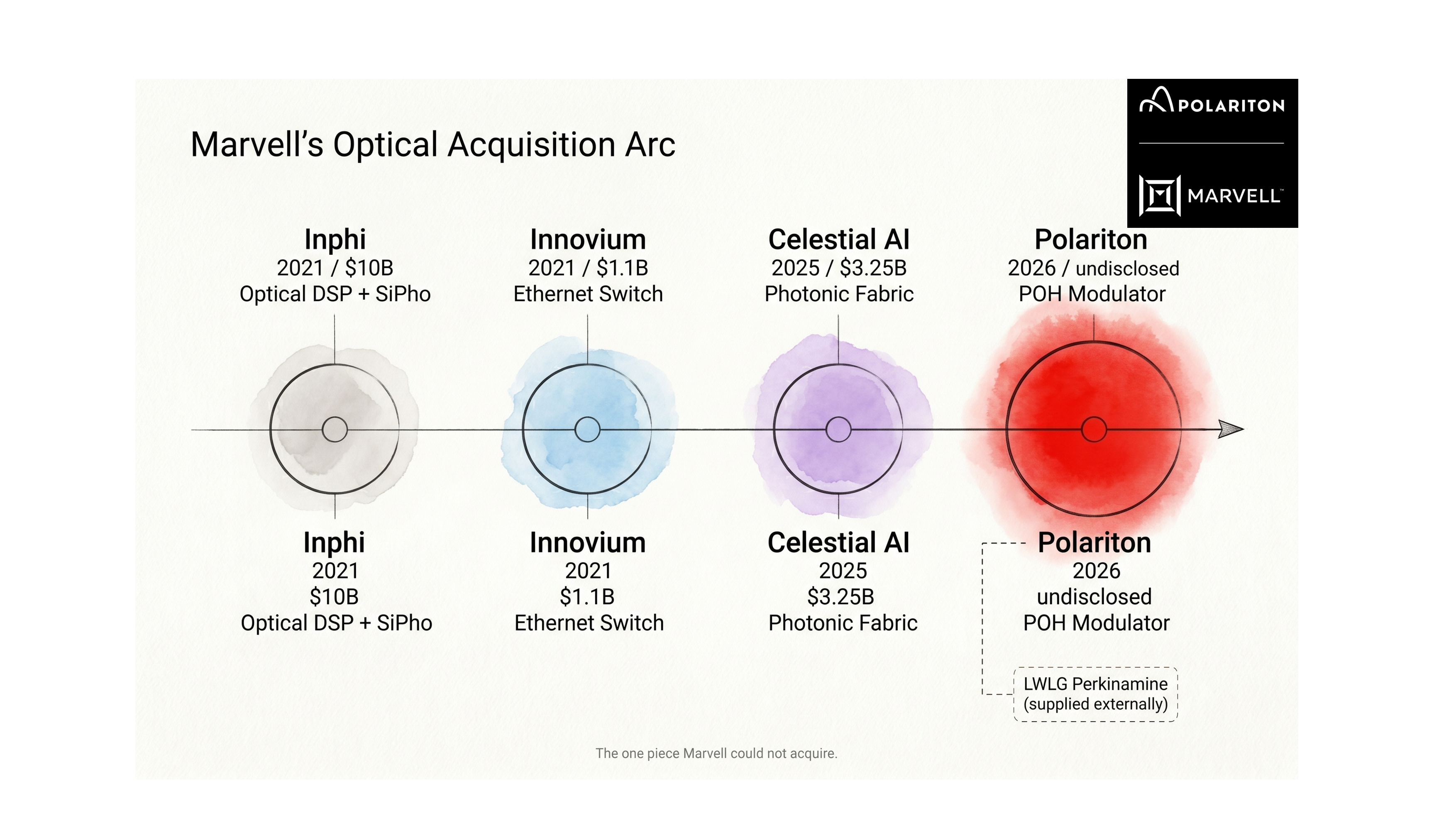
Marvell has made four optical-related acquisitions over the past five years.
2021: Inphi ($10B), coherent DSP and silicon photonics full stack [1]
2021: Innovium ($1.1B), Ethernet switch silicon [2]
2025.12: Celestial AI ($3.25B + $2.25B milestones), Photonic Fabric, scale-up optical interconnect [3]
2026.4: Polariton Technologies (undisclosed), plasmonic modulator [4]
Here is what stands out. The Inphi deal put Marvell at the top of the optical DSP industry. The Celestial AI deal secured a scale-up architecture position. Polariton is different. It is the first acquisition where Marvell bets on device-level modulation technology itself. The direction is clearly distinct.
The press release names the explicit target as “3.2T and beyond,” with coherent and DCI applications like ZR/ZR+ called out specifically [4]. In other words, this is a technology grab for the generation beyond the already-guided 1.6T.
2. Who Polariton Is
Polariton Technologies is a Swiss company that spun out of Prof. Jürg Leuthold’s group at ETH Zurich in 2019 [5]. The company holds the distinction of being the first in the world to commercialize plasmonics-based electro-optic products [6].
All three co-founders were PhDs from Leuthold’s group: CEO Claudia Hoessbacher (measurement and characterization), co-CTO Wolfgang Heni (devices), and Benedikt Bäuerle (system engineering). Leuthold himself worked at Bell Labs from 1999 to 2004 on III-V and silicon photonics high-speed communication devices, and currently leads the Institute of Electromagnetic Fields (IEF) at ETH Zurich [7].
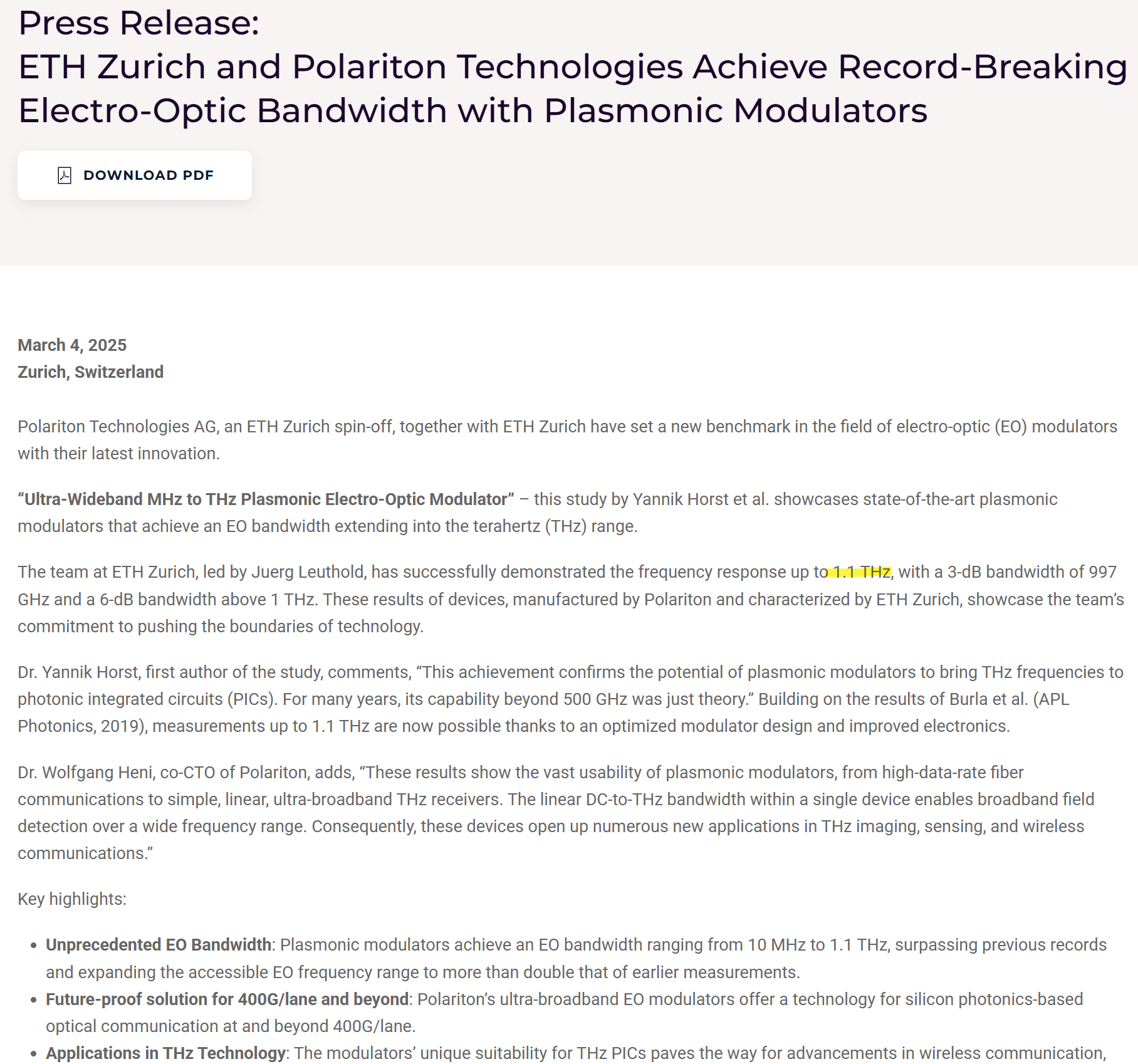
The product line consists of PICs (Photonic Integrated Circuits) implementing plasmonic Mach-Zehnder and ring resonator modulators on a silicon photonics platform. They support both 1310nm and 1550nm, and also offer a custom design service [5]. In 2024, the company characterized MZMs and IQ modulators up to 145 GHz [6], and in early 2025, together with ETH Zurich, they published a record of EO bandwidth measured up to 1.1 THz in Optica [8].
Cignal AI’s Optical Component Startup Tracker describes Polariton as rivaling TFLN at bandwidths above 145 GHz, and exceeding current SiPho and InP capabilities [9].
3. A Decade of Plasmonics: Hype, Cooldown, and Quiet Commercialization
Personally, this is the most interesting part of the story, so I will spend a bit more space here.
Early-to-Mid 2010s, Plasmonics Was Genuinely Hot
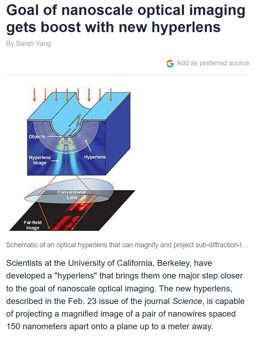
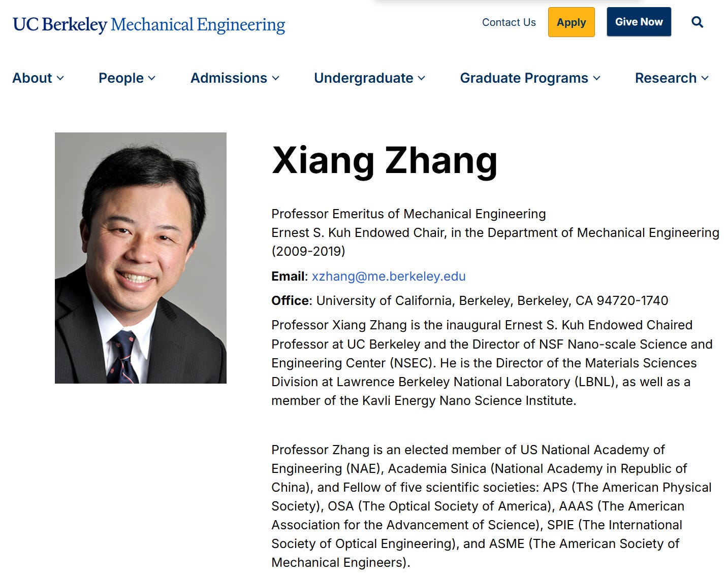
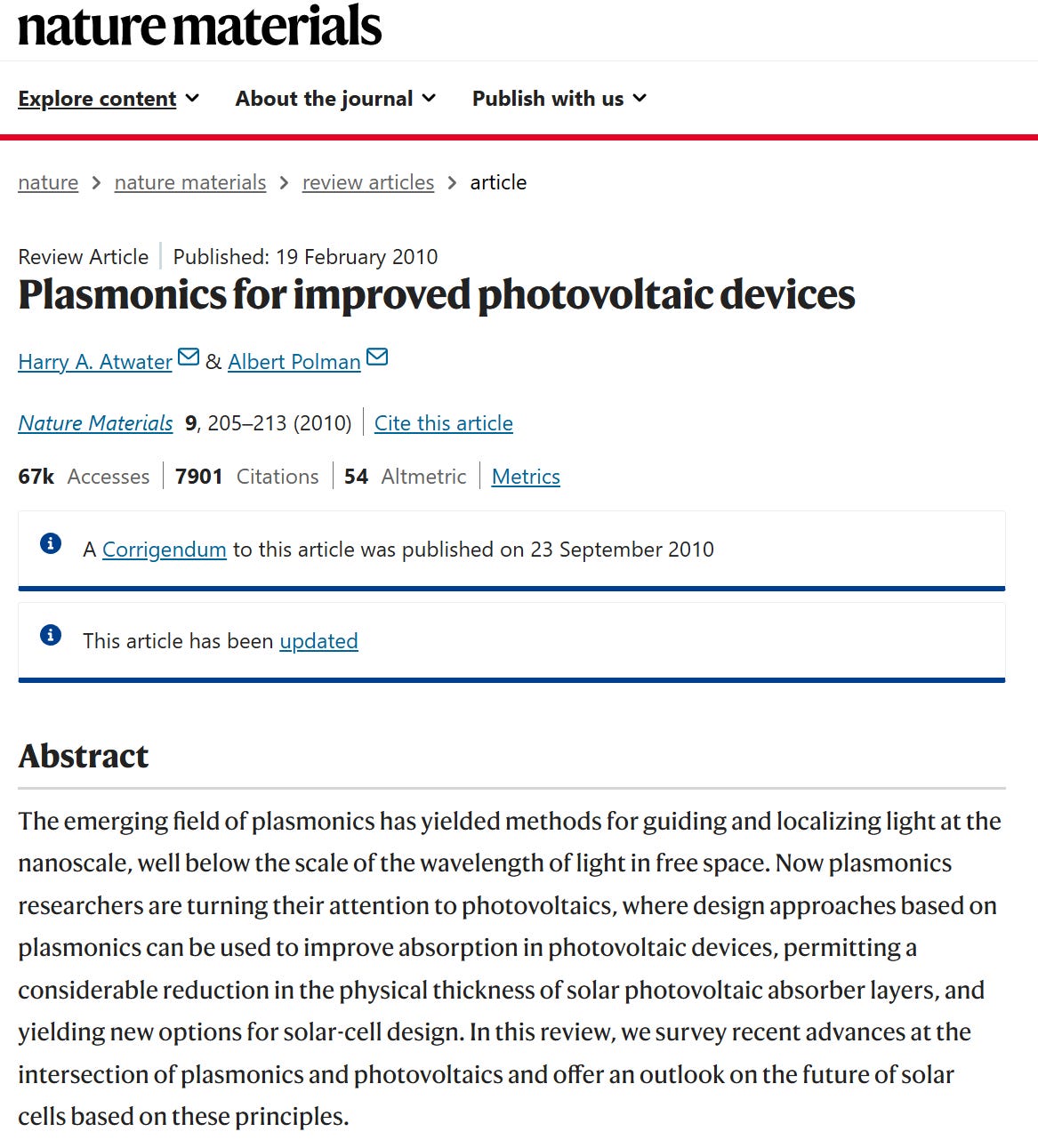
I remember the atmosphere when UC Berkeley’s Xiang Zhang group published their hyperlens paper in Science in 2007 [10]. The idea of stacking metal thin films to break the optical diffraction limit. The following year the same group published 3D negative-index metamaterials in Nature, and Discover and Time picked it as one of the innovations of the year [11]. Caltech’s Harry Atwater proposed plasmonic solar cells in Nature Materials around the same time [12], and Stanford’s Mark Brongersma was working on plasmonic waveguides.
Half the keynotes at every conference were about plasmonics. Surface plasmon polaritons, the spaser (plasmonic laser), metamaterial cloaks, negative refraction, hyperlenses, plasmonic solar cells, sub-diffraction imaging. Just reading the titles, it felt like the world was about to change within ten years.
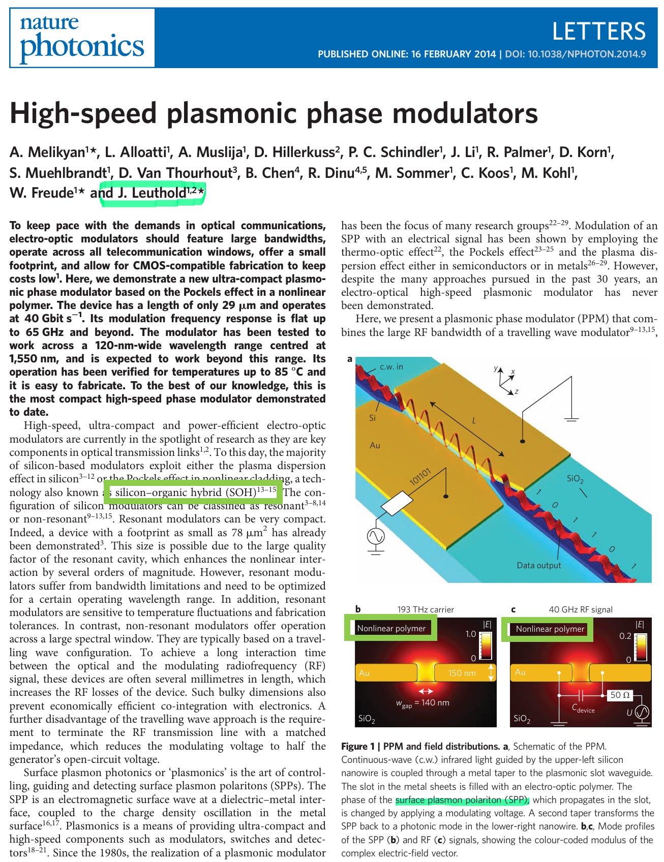
Leuthold’s group was part of this wave too. Starting at KIT and later moving to ETH Zurich, the group published a plasmonic absorption modulator in Optics Express in 2011 [13], then in 2014 published a “29 µm long, 65 GHz bandwidth” phase modulator in Nature Photonics [14]. Christian Haffner from the same group published a 10 µm all-plasmonic Mach-Zehnder modulator in Nature Photonics in 2015 [15], followed by a “low-loss plasmon-assisted” modulator in Nature in 2018 [16]. Polariton was founded in 2019 on top of this technology stack.
Then the Funding Dried Up
Around 2017 to 2018, the mood shifted. Plasmonics got pegged as “attractive in principle but unclear as a commercial path.” The reason came down to one thing: metal loss. Compressing light into nanometer scales requires using collective electron oscillations at a metal surface, but that means photons get absorbed into the metal, adding significant insertion loss. Over tens of centimeters of fiber link, this is fatal.
NSF and DARPA plasmonics grants shrank meaningfully, and many researchers pivoted toward metasurfaces, topological photonics, quantum plasmonics, and 2D materials. By the early 2020s, the industry perception had settled on “plasmonics is a technology that ended at the research stage.” Xiang Zhang himself moved to become Vice-Chancellor of the University of Hong Kong, so his academic position shifted as well.
But the ETH Zurich Group Kept Going
This is the part I personally find most admirable. The Leuthold group took the metal loss problem head-on, combined it with polymer-based Pockels effect into a POH (plasmonic-organic hybrid) path, and kept pushing. Melikyan 2014, Haffner 2015, Ayata 2017 (Science, single metal layer), Haffner 2018 (Nature, low-loss), Heni 2019 (Nature Communications, attojoule IQ modulator) [17]. Each paper pushed bandwidth up, reduced power, cut loss, shrank footprint.
Polariton was founded in 2019. MZMs and IQ modulators were characterized up to 145 GHz in the early-to-mid 2020s. In 2025, the 1.1 THz measurement with ETH came [8]. While the community thought the technology was done, one group in Switzerland quietly kept breaking bandwidth records.
4. Six Modulator Platforms, Side by Side
To understand what the Polariton acquisition really means, you need to see the current high-speed optical modulator landscape. No single platform is outright best. Each carries different trade-offs.
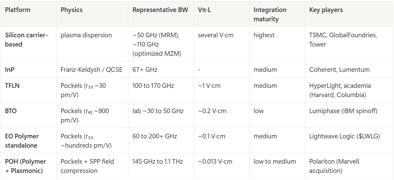
Let me walk through each.
Silicon carrier-based is the workhorse for AI data center optical modules today. It relies on the plasma dispersion effect (free-carrier density shifts change both refractive index and absorption), but this is not pure phase modulation, so chirp is intrinsic. That said, mature CMOS foundry infrastructure and 200mm / 300mm wafer ecosystems make it the cheapest platform to produce.
InP is a III-V semiconductor platform where EAMs are built on Franz-Keldysh or quantum-well (QCSE) effects. It has the advantage of native integration with lasers, but heterogeneous integration with silicon photonics is process-heavy. Coherent and Lumentum have used this technology for many years.
TFLN (thin-film lithium niobate) is a platform where a LiNbO₃ thin film is bonded onto silicon via “smart-cut” processing. It allows pure phase modulation through the Pockels effect, and achieves both wide bandwidth and CMOS-compatible drive voltage. This is why it has been the most watched next-gen candidate in recent years. However, smart-cut wafer supply is still stuck at 6 inch (NanoLN, Partow, NGK, SRICO), and foundry integration still needs time.
BTO (barium titanate) has a Pockels coefficient r₄₂ around 900 pm/V, roughly 30 times that of LiNbO₃ (30 pm/V). In principle, it is one of the most attractive EO materials available [18]. IBM Zurich has studied it for years, and the spinoff Lumiphase was founded in 2020 [19]. However, epitaxial growth of BTO films on silicon is complex (it requires a SrTiO₃ buffer layer and careful crystallographic orientation control). BTO Mach-Zehnder modulators have reached Vπ·L of 0.2 V·cm [20], but foundry maturity is still early.
EO Polymer standalone applies organic chromophores with extremely high Pockels coefficients via spin coating on silicon. It is compatible with back-end-of-line processing, and with Vπ·L around 0.1 V·cm, sub-volt drive is possible. The lead player is Lightwave Logic (NASDAQ: LWLG). The company’s Perkinamine polymer recently demonstrated 200 Gbps per lane and passed Telcordia 85/85 (85℃, 85% humidity) reliability testing [21]. Polymers historically had weaknesses in thermal, moisture, and photo stability, but as these have improved, 2025 marks the year the technology entered a commercialization path. The broader polymer EO modulator ecosystem and the competitive landscape (NLM Photonics and others) were analyzed in detail in our earlier article The Next Materials War in Silicon Photonics: Polymer EO Modulators, Who Wins? [22].

POH (Plasmonic-Organic Hybrid) is today’s main character. At the physics level, it is an EO polymer injected into a plasmonic slot. A metal-organic-metal slot compresses the electromagnetic field down to nanometer scale, and the EO polymer inside the slot shifts the phase with extreme efficiency. The analogy: take an already powerful EO polymer and confine it inside a very narrow nozzle, so the same input produces a much larger output. Polariton’s plasmonic IQ modulator has an active section of 4×25 µm × 3 µm [17], with 0.07 fJ/bit at 50 Gbit/s and 2 fJ/bit at 400 Gbit/s. Considering that standard silicon modulators need tens of mm of active section and pJ-scale energy, the orders of magnitude are different.
Metal loss remains a real issue. Insertion loss is larger than for standard silicon modulators or TFLN. That said, the Leuthold group has spent 15 years bringing it down from tens of dB into the single-digit dB range, and it has now entered the practical range.
There is one more variable worth calling out here. Marvell’s Polariton acquisition does not fully internalize the POH modulator stack. One critical piece remains outside what Marvell could buy, and because of that piece, this acquisition quietly repositions another publicly traded company. Let me unpack it below.
