
Mapping the AI Landscape with Light: How OCS Transforms the Data Center Physical Layer

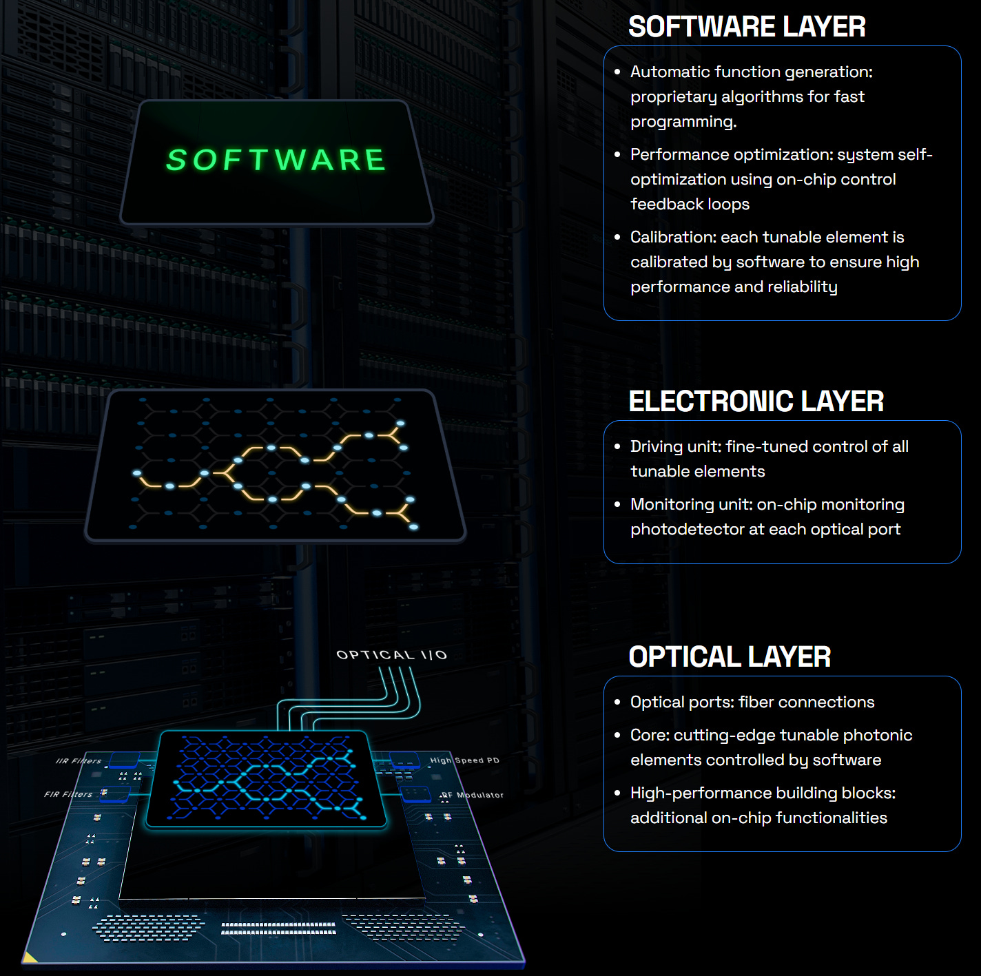
1. OCS (Optical Circuit Switching) Definition and Principles
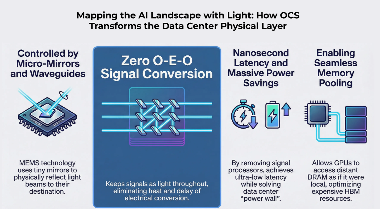
Definition: A Layer 1 switching technology that reroutes paths at the optical signal level without Optical-Electrical-Optical (O-E-O) conversion.
Operating Mechanisms:
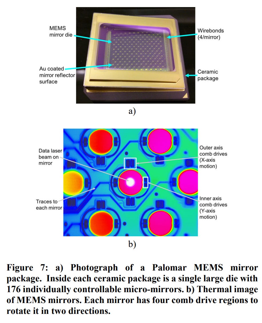
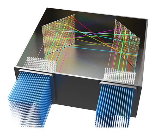
MEMS Approach: Uses micro-mirrors to physically reflect light beams (e.g., Google Apollo, Lumentum).
SiPh & SOA Approach: Controls light paths via on-chip waveguides and semiconductor optical amplifiers (e.g., Salience Labs, iPronics).
Performance Metrics:
Insertion Loss: Modern units target 1.0dB to 2.0dB for high-efficiency connectivity.
Switching Speed: MEMS operates in the ms range, while SOA/SiPh achieves ns to μs range for ultra-fast reconfiguration.
Bandwidth Transparency: OCS is independent of data baud rates, making it future-proof for 1.6T and beyond.
2. Strategic Deployment Areas
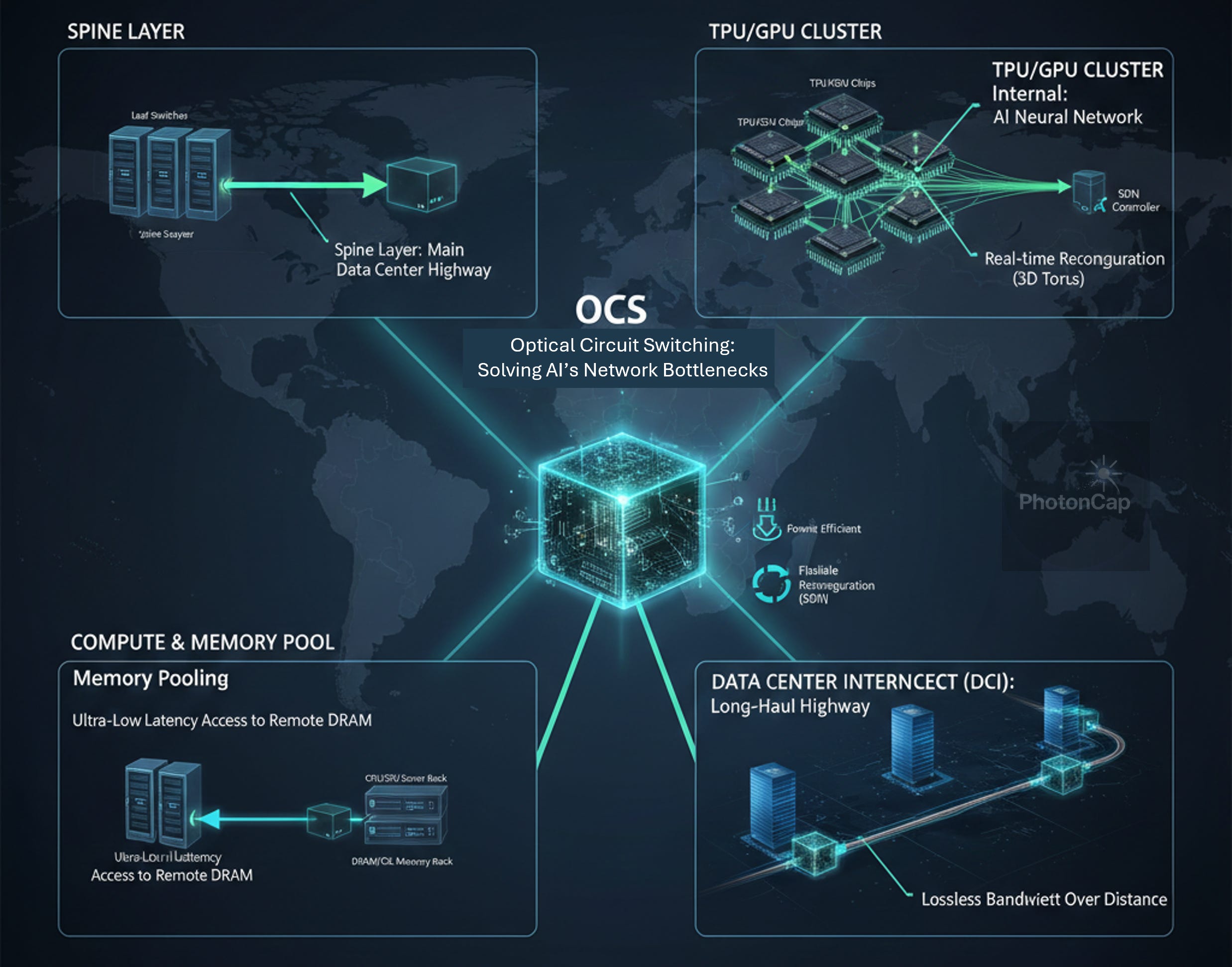
Spine Layer (Main Highway): Located at the backbone to interconnect Leaf/ToR switches; reduces power and cost by >40%.
TPU/GPU Clusters (Neural Network): Enables Inter-Chip Interconnects (ICI) for 3D Torus topologies and real-time fault recovery.
Compute-to-Memory Fabric (Memory Pooling): Core infrastructure for Memory Tiering; allows servers to access remote DRAM/CXL with local-like latency.
Data Center Interconnect (DCI): Serves as a long-haul highway between separate DC buildings to minimize bandwidth loss.
3. Technical Rationale: Why OCS Now?
Power/Thermal Wall: AI scaling has pushed traditional electronic switching to its thermal limits.
Network Scalability: Optical signals maintain integrity over longer distances, ideal for massive GPU clusters.
Dynamic Reconfigurability: Software-defined control allows for physical topology changes without manual recabling.
4. Key Applications: Memory Tiering and Resource Allocation
DRAM Pooling: Optimizes the ratio of expensive HBM by utilizing remote DRAM via low-latency OCS paths, a key component of Google’s next-gen architecture.
Dynamic Allocation: Enables Software-Defined Networks (SDN) to reconfigure physical network topologies in real-time based on specific workload requirements.
Summary: “A next-generation networking technology that resolves AI communication bottlenecks using light and mirrors instead of electricity.”
5. Key Players and Ecosystem
(1) Google
Developed Project Apollo (OCS) in-house with a vertically integrated SDN interface.
Increased throughput by 30%, use 40% less power, incurs 30% less Capex, reduces flow completion by 10%, and delivers 50x less downtime across their network.

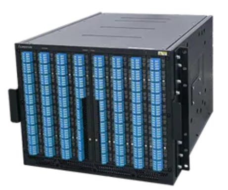
(2) Lumentum
Recognized Google’s primary hardware partner for OCS deployment.
Co-leads the OCP OCS Sub-project to standardize optical switching infrastructure. (https://ipronics.com/ipronics-and-lumentum-lead-the-efforts-to-standardize-ocs-alongside-key-industry-players/)
https://www.lumentum.com/en/products/300x300-optical-circuit-switch-ocs
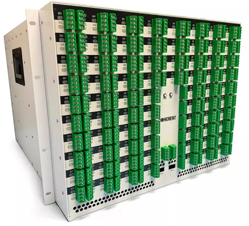
(3) Coherent
Utilizes Liquid Crystal (LCOS) technology; won the ECOC 2024 Innovation Award. (https://www.coherent.com/networking/optical-circuit-switch)
Supports diverse configurations including 64x64 and 320x320 matrices.
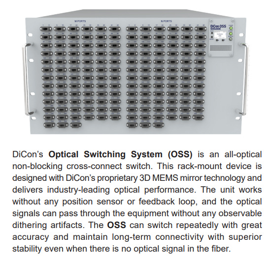
(4) DiCon Fiberoptics
Offers 3D MEMS supporting up to 600x600 ports with ultra-low loss.
Focused on high-reliability sectors including Quantum Computing and Defense. (https://www.diconfiberoptics.com/products/Solutions-Network-Management-Cyber-Security-OSS.php)
(5) iPronics
Pioneered FPPGA (Field Programmable Photonic Gate Array) technology.
Co-leads OCP OCS standardization; enables software-defined, reconfigurable optical paths.


(https://arxiv.org/pdf/2404.08648, Journal of Optical Communications and Networking 16.8 (2024) https://doi.org/10.1364/JOCN.521505)
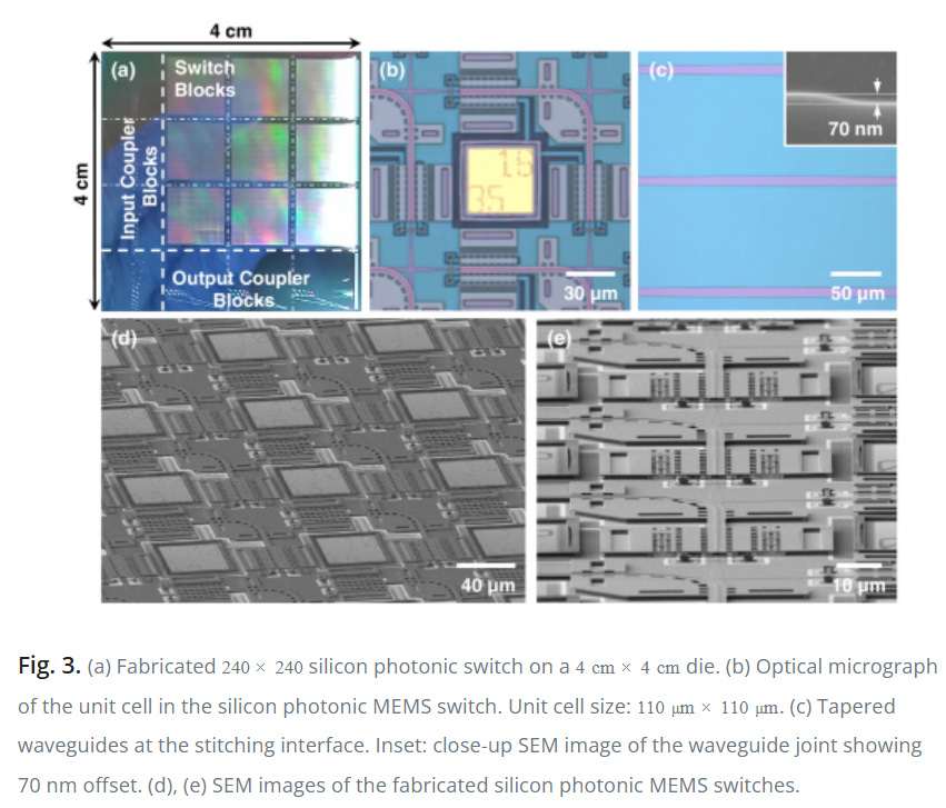
(6) nEye.ai
Developed Silicon Photonics MEMS for high-density interconnects.
Backed by NVIDIA, Microsoft (M12), and Micron.
Joined OCS project (https://www.opencompute.org/blog/the-open-compute-project-announces-new-optical-circuit-switching-ocs-project)(https://www.opencompute.org/blog/the-open-compute-project-announces-new-optical-circuit-switching-ocs-project)
https://doi.org/10.1364/OPTICA.6.000490 (co-founder Dr. Tae Joon Seok’s paper)

(7) Salience Labs
Leveraging SOA (Semiconductor Optical Amplifier) for low-latency, loss-compensated switching.
Backed by Applied Ventures to drive energy-efficient AI data centers. (https://www.appliedmaterials.com/us/en/newsroom/perspectives/optical-circuit-switches-show-promise-more-energy-efficient-ai.html)