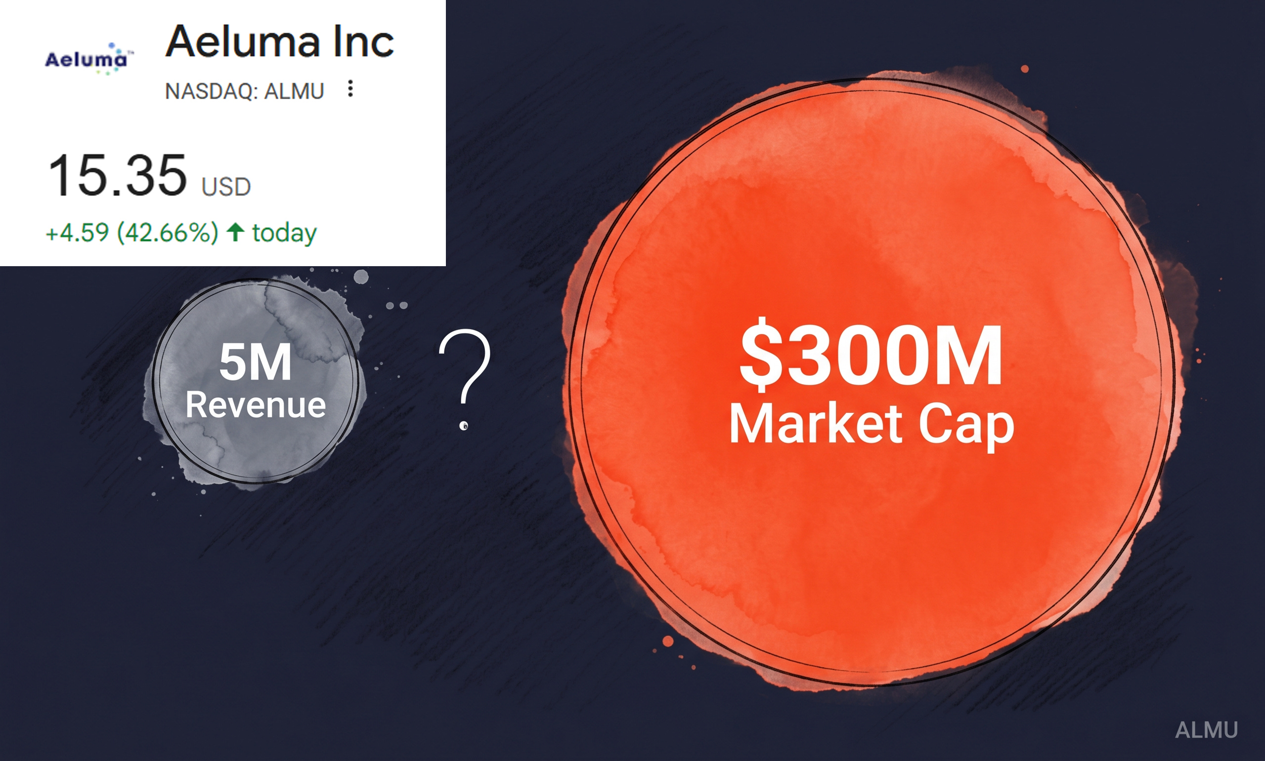
$5M Revenue, $300M Market Cap: What Does Aeluma Actually Sell?
Government R&D contracts, UCSB papers, and zero commercial customers

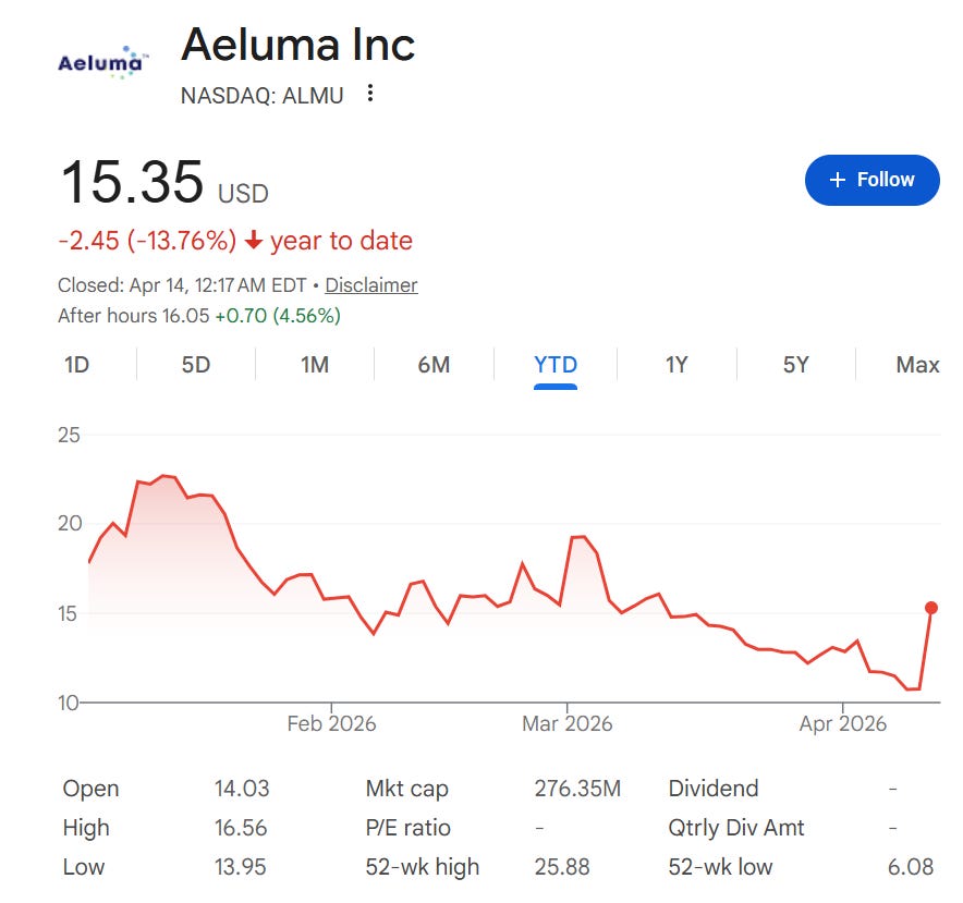
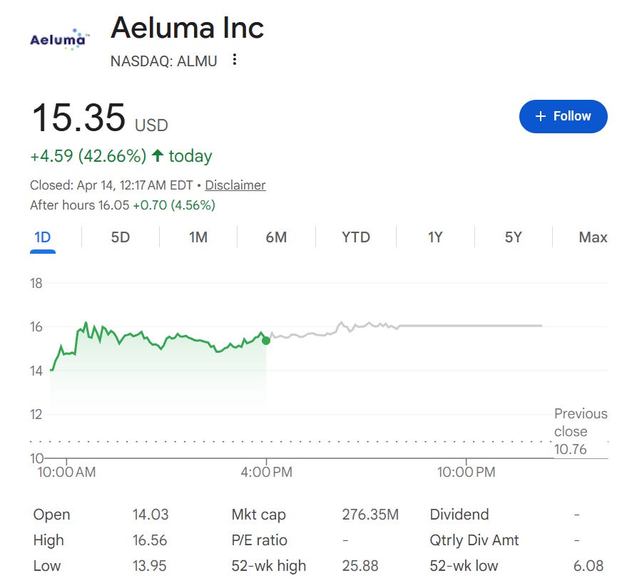
A $5M-revenue company is trading at a $300M market cap. Aeluma (NASDAQ: ALMU) is developing a III-V-on-silicon platform centered on direct heteroepitaxy via MOCVD, with complementary wafer bonding work. On April 13, the company announced $4M in U.S. government contracts alongside manufacturing partnerships with Tower Semiconductor and Sumitomo Chemical, sending shares up over 40% intraday [2]. This article, a follow-up to our earlier comparison of three SiPho light source microcaps [1], is a standalone deep dive into Aeluma’s technology platform, its competitive positioning against Quintessent (which uses a different integration approach and targets a different market), and the valuation gap between government R&D validation and commercial reality. The technology is real. The commercial proof is not.
$ALMU, TSEM 0.00%↑
Contents
Intro: $4M Contract, 40%+ Surge, and What It Means
Background: Silicon Cannot Make Light
Aeluma’s Platform: What They Actually Make, and What Remains R&D
The Competitive Landscape: Different Technology, Different Market
Commercialization Path and Gap Analysis (paid)
Financials, Valuation, and Risk Asymmetry (paid)
Closing
References & Sources
1. Intro
A $5M-revenue company is trading at a $300M market cap.
Aeluma (NASDAQ: ALMU) announced $4M in U.S. government contracts on April 13, and shares jumped over 40% intraday [2]. The contracts fund the scaling of quantum dot lasers and AlGaAs nonlinear photonics, with wafer production handled by Tower Semiconductor and Sumitomo Chemical Advanced Technology [2]. One thing to note upfront: the company’s own press release describes this as scaling its “heterogeneous integration platform,” not as a monolithic laser commercialization milestone.
I covered Aeluma earlier this year alongside QD Laser and Sivers Semiconductors in a comparison of three SiPho light source microcaps [1]. My conclusion then: “The most ambitious approach of the three, but the path to commercial production is the most uncertain.”
The Silicon Photonics Light Source War: Same Problem, Three Solutions (Small Cap)

Intro Sivers Semiconductors (OTCMKTS: SIVEF) surged +63.62% and QD Laser (TYO: 6613) jumped +33.39% over the past five days. What do these two microcaps have in common? They’re both light source suppliers for silicon photonics (SiPho).
Same conclusion now. The reasons are just clearer.
The question is not whether the technology works. It does. The question is whether Aeluma can turn government R&D into recurring commercial revenue. Everything in this article is organized around that question.
Key takeaway: A $4M government contract triggered a 40%+ intraday move. The technology is real, but the market is pricing in an unproven future.
2. Background: Silicon Cannot Make Light
This section recaps what I covered in detail in the previous article [1]. The short version:
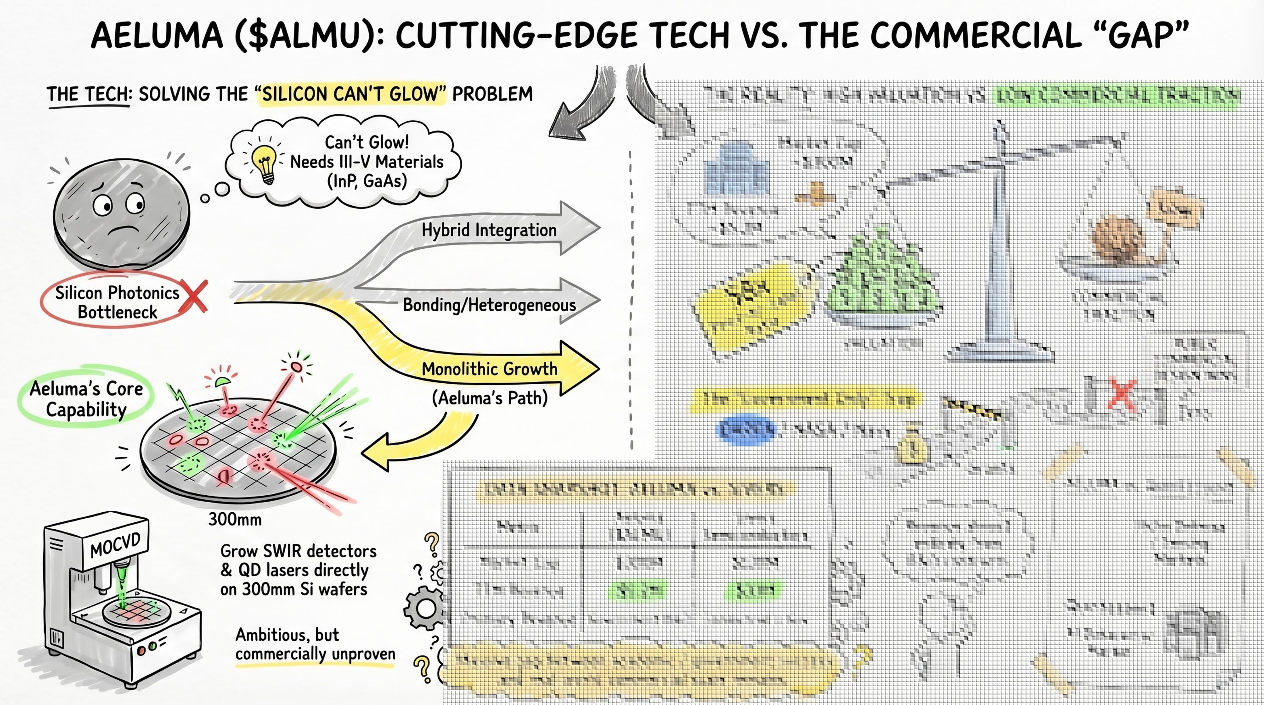
Silicon photonics (SiPho) has a fundamental weakness. Silicon is an indirect bandgap material. It can guide light, modulate it, even detect it (with germanium). But it cannot efficiently generate light. Every SiPho chip needs a III-V compound semiconductor laser (InP, GaAs, etc.) attached from the outside.
There are three ways to attach that laser.
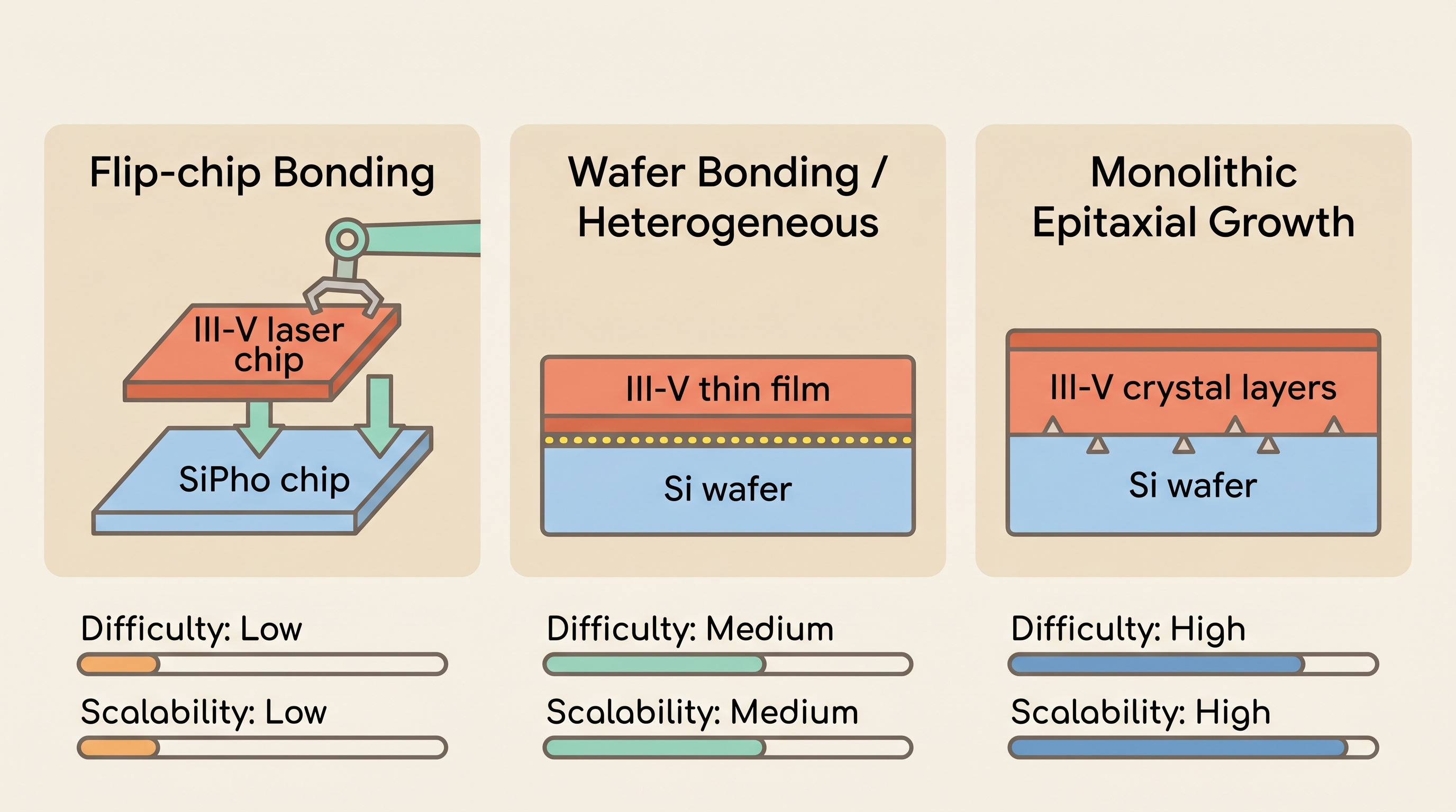
Method 1: Flip-chip bonding. Build the III-V laser separately, then pick and place it onto the SiPho chip. Think of it like snapping Lego bricks together. Most commercial transceivers use this today. It works, but each chip needs individual alignment. Cost and yield hit ceilings.
Method 2: Wafer bonding (heterogeneous integration). Bond III-V material onto silicon at the wafer level, then process lasers on top. Intel shipped millions of SiPho transceivers this way [3]. Quintessent and Tower Semiconductor have partnered to add quantum-dot lasers and optical amplifiers to Tower’s PH18 silicon photonics foundry platform [4]. Better scalability than Method 1, but the bonding step itself has yield and cost challenges.
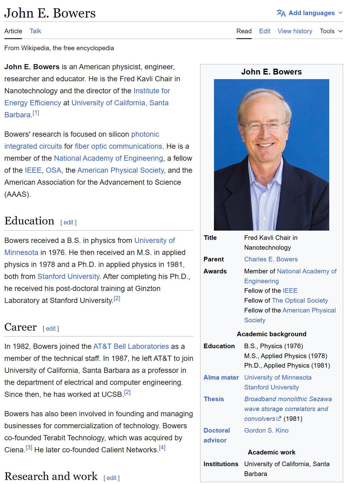
Method 3: Monolithic epitaxial growth. Grow III-V material directly on the silicon wafer, crystal layer by crystal layer. No bonding step. In theory, you can use existing CMOS fab lines. The ultimate solution for scalability and cost. But lattice mismatch, polarity mismatch, and thermal expansion mismatch between III-V and silicon create crystal defects that destroy device performance and lifetime [5]. Despite decades of academic progress (notably from UCSB’s Bowers Lab [7]), no one has commercialized this approach. It remains a research frontier.
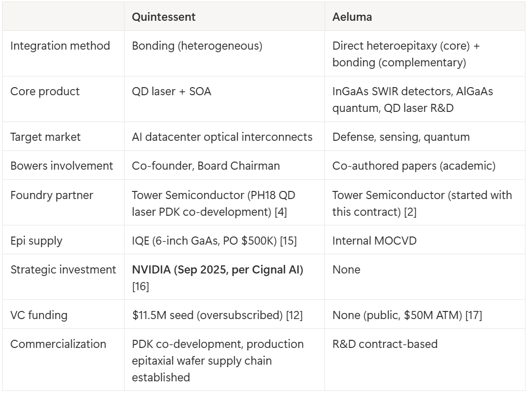
Aeluma’s core technical differentiation is monolithic heteroepitaxy (Method 3): growing III-V materials directly on silicon via MOCVD. This applies to its InGaAs SWIR photodetectors and its QD laser R&D with AIM Photonics [9][14]. However, certain platform extensions use wafer bonding (Method 2) as a complementary route. The AlGaAs quantum photonics work with Thorlabs, for example, uses direct wafer bonding [11]. The company markets its overall platform under the umbrella term “heterogeneous integration” [2], which covers both approaches.
Quintessent uses Method 2 (wafer bonding) to integrate QD lasers and SOAs onto Tower’s PH18 SiPho foundry platform [4].
The difference between these two companies is both technical and commercial.
Key takeaway: Three paths exist for SiPho light source integration. Aeluma’s core is direct heteroepitaxy (Method 3) with some complementary bonding work. Quintessent uses bonding (Method 2). The differentiation is real, but so is the gap in commercial readiness.
3. Aeluma’s Platform: What They Actually Make, and What Remains R&D
3-1. Aeluma’s Dual-Track Platform
Aeluma’s product platform spans two integration approaches.
Direct heteroepitaxy (Method 3, core competency):
InGaAs SWIR photodetectors. Klamkin’s published work demonstrates InGaAs photodiodes grown directly on CMOS-compatible silicon by MOCVD heteroepitaxy, achieving low dark current, high responsivity, and GHz-class bandwidth. This is direct growth, not bonding. Target applications include defense ISR, industrial sensing, LiDAR, and other SWIR imaging use cases [9].
QD laser R&D. Aeluma collaborates with AIM Photonics and UCSB on monolithic QD laser integration using MOCVD selective area growth on 300mm SiPho wafers [10][14]. A 2025 ACS Photonics paper demonstrated monolithic QD photodetector + QD laser integration on silicon photonics, with Klamkin and Bowers as co-authors [14]. Academically significant, but still a government-directed research project at this stage.
Wafer bonding (Method 2, complementary track):
AlGaAs nonlinear photonics. In May 2025, Aeluma and Thorlabs demonstrated wafer-scale AlGaAs integration on 200mm CMOS silicon using direct wafer bonding [11]. This platform targets quantum communication and sensing. Today’s $4M government contract partially funds this work [2].
Aeluma’s MOCVD capability for growing high-quality III-V epi on wafers up to 300mm is the company’s real technical asset [9]. The company markets its overall platform under the umbrella term “heterogeneous integration,” but the core differentiation is direct heteroepitaxy.
3-2. Why Direct Heteroepitaxy Is Hard (Context)
A brief detour on why Method 3 has not been commercially deployed at scale. This matters because Aeluma’s core competency sits in this space.
GaAs and silicon have a ~4% lattice mismatch [5]. At the atomic level, 4% is enormous. Imagine tiling a floor with two sets of tiles that differ by 4% in size. At every seam, you get gaps or overlaps. In semiconductor terms, those gaps are threading dislocations (TDD), crystal defects that propagate through every layer above them.
Additional problems include polarity mismatch (silicon is non-polar, GaAs is polar, creating antiphase boundaries) and thermal expansion mismatch (causing cracking during cooldown) [5][6]. These are the fundamental challenges Aeluma’s MOCVD heteroepitaxy must overcome.
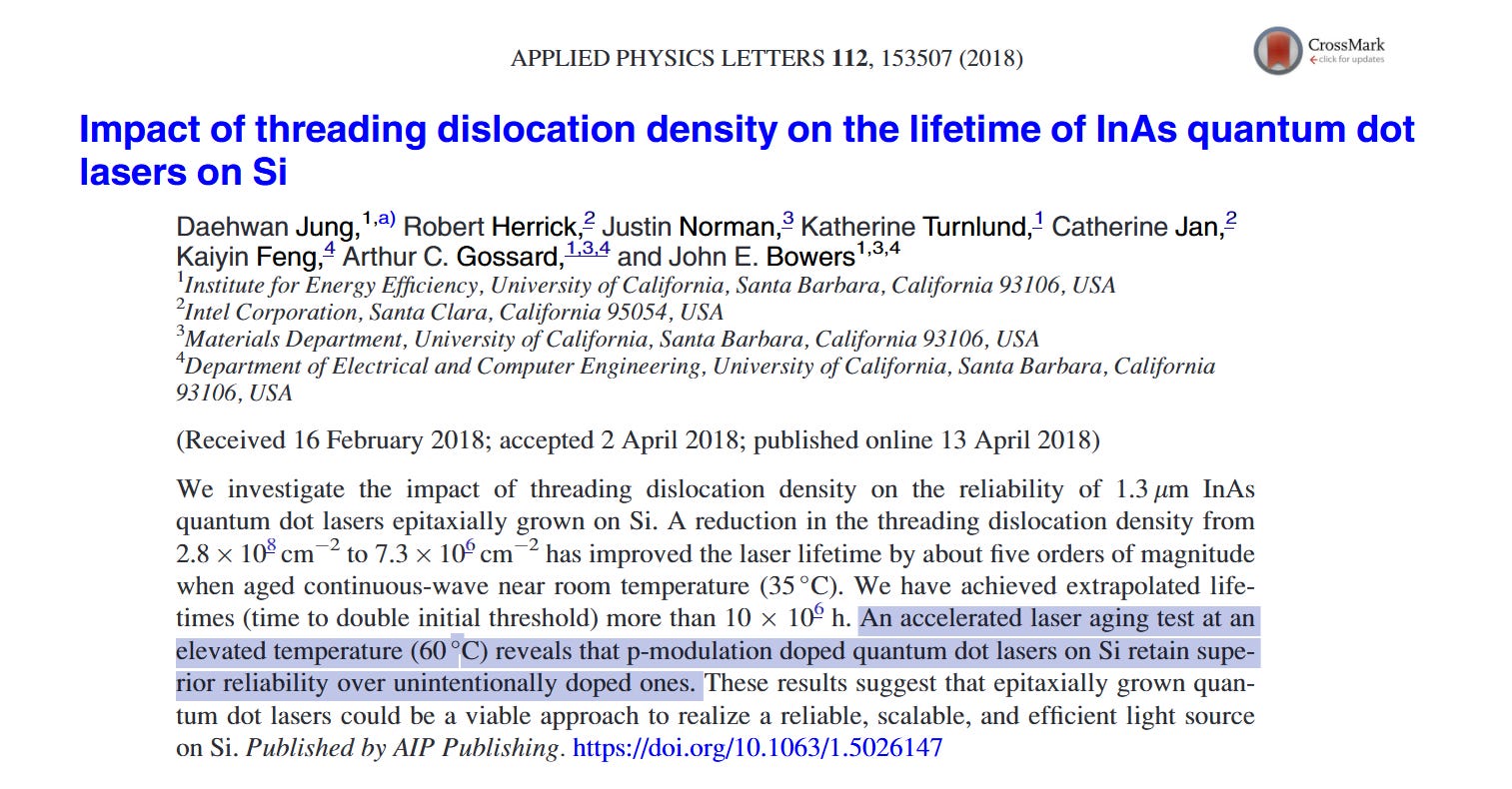
Quantum dots (QDs) help. QDs are nanometer-scale 3D structures that confine carriers, reducing their probability of diffusing to nearby dislocations [7]. The UCSB Bowers group has shown extrapolated lifetimes exceeding 10 million hours at room temperature (35C) by reducing TDD to 7.6x10^6 cm^-2 [5]. But elevated-temperature results are far more sobering: the p-modulation doped sample showed roughly 65,000 hours at 60C [5], and Telcordia GR-468 qualification requires 20+ years at 80C. A 2025 all-MOCVD paper achieved 20-year lifetime at 55C [8], but 55C and 80C are meaningfully different under Arrhenius scaling.
The bottom line: direct heteroepitaxy of III-V on silicon is progressing, but commercial-grade qualification at operating temperatures has not been demonstrated.
3-3. So What Is Aeluma Actually Selling?
This is where the investment judgment splits. Aeluma’s revenue comes almost entirely from government R&D contracts [18]. The partner list (UCSB, AIM Photonics, Thorlabs, NASA, DARPA, Navy, DOE) validates academic and strategic merit. It does not validate commercial manufacturing capability or product-market fit.
The question for investors is not whether Aeluma’s MOCVD heteroepitaxy capability is technically real. It is. The question is: who is buying it outside of government?
Key takeaway: Aeluma’s core is direct heteroepitaxy (InGaAs detectors, QD laser R&D), with AlGaAs bonding as a complementary track. The technical differentiation is real. Revenue is almost entirely government contracts. The gap is not physics. It is commercial demand.
4. The Competitive Landscape: Different Technology, Different Market
4-1. Two Companies from the Same Ecosystem
The academic center of III-V quantum dot lasers on silicon is John Bowers’ lab at UC Santa Barbara. Bowers demonstrated the world’s first hybrid silicon laser with Intel in the mid-2000s [3] and has authored most of the foundational papers in this field.
Two commercial spinouts emerged from this ecosystem, taking different technical and commercial paths.
Quintessent (private, founded 2019). Co-founded by John Bowers himself, who is Board Chairman. CEO is Alan Liu, a Bowers Lab PhD graduate [12]. Product: QD lasers and semiconductor optical amplifiers (SOAs) integrated into Tower’s PH18 SiPho foundry platform [4]. Target market: AI datacenter optical interconnects.
Aeluma (NASDAQ: ALMU, founded 2019). Founded by Jonathan Klamkin, also a UCSB photonics professor [13]. Klamkin has co-authored multiple papers with the Bowers group [14]. Product: InGaAs SWIR detectors, AlGaAs quantum photonics. Target market: defense, aerospace, quantum, sensing.
4-2. The Real Comparison
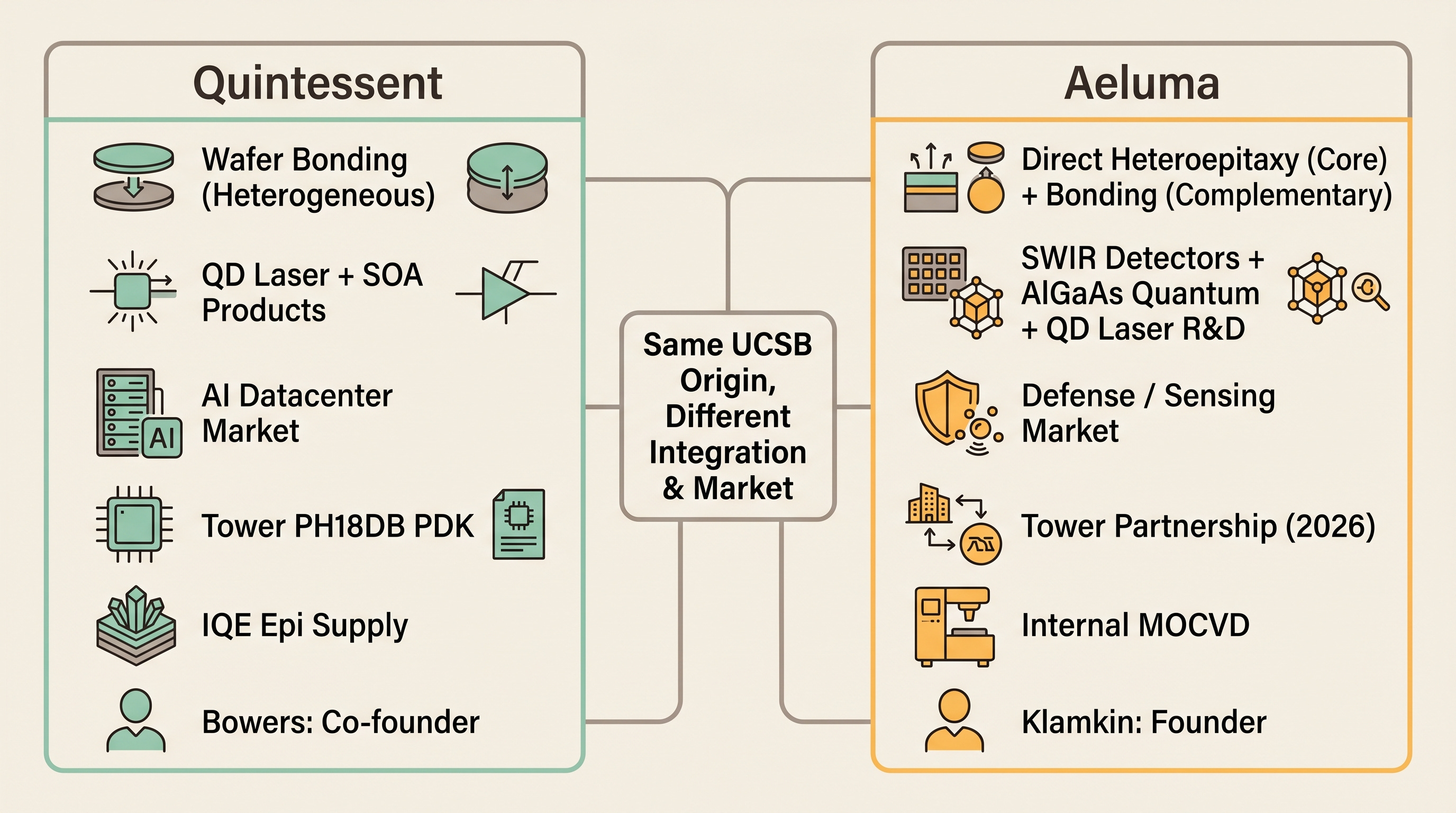
The difference between these two companies is both technical and commercial.
Quintessent is building QD lasers for the AI datacenter optics market using wafer bonding on Tower’s PH18 SiPho foundry platform. This is the market where NVIDIA is investing $4B in optical supply chains. Quintessent has a product (laser + SOA), a foundry PDK, and an epi supply chain (IQE) [15].
Aeluma is building III-V-on-silicon devices via direct heteroepitaxy, targeting government and defense markets. Its revenue is almost entirely from DARPA, NASA, Navy, and DOE contracts. Products include InGaAs SWIR detectors (grown by heteroepitaxy) and AlGaAs quantum photonics (bonding-based). QD laser work is an R&D collaboration with AIM Photonics, not yet a commercial product.
This is why the Bowers signal matters. Bowers chose to commercialize QD lasers for AI datacenters through Quintessent, using bonding. Aeluma’s direct heteroepitaxy approach is technically more ambitious, but Quintessent’s product-market story is cleaner and more immediately underwritable.
Aeluma is pointing at a different target: government photonics and sensing. Those markets are real, but they are smaller and slower-moving.
The technology alone makes Aeluma hard to dismiss. But the market is pricing “who reaches volume photonics markets first,” not “who has the best epi capability.” And on that question, Quintessent has clearer positioning.
Key takeaway: The difference between Aeluma and Quintessent is both technical and commercial. Aeluma’s core is direct heteroepitaxy targeting defense/sensing. Quintessent uses bonding to build QD lasers for AI datacenters. Bowers chose the volume market. The $300M market cap is pricing in a commercial transition that has not started.